Recommended
PPTX
PPTX
Graphene material for aerospace technology
PDF
Progress in Synthesis of Graphene using CVD, Its Characterization and Challen...
PDF
Graphene: its increasing economic feasibility
DOCX
PPTX
Graphene 140416111416-phpapp02
PDF
Recent development in graphene technology for multidiscilinary properties and...
PPTX
Graphene and its future applications
PDF
631332_2_merged_1423441293
PPTX
PPTX
PPTX
PDF
PDF
PDF
PDF
Graphene materials for opto and electronic applications 2014 Report by Yole D...
PPTX
UG CNSE Capstone Project 2016
PPTX
PDF
EMERGING ENERGY OF GRAPHENE
PPTX
PDF
Graphene is an atomically thin sheet of carbon atoms arranged in a hexagonal ...
PDF
PDF
NOVO MODISMO ACADÊMICO E A PROMESSA DE APLICAÇÃO INDUSTRIAL DE GRAFENO
PPTX
PPT
PPT
GRAPHENE SYNTHESIS AND APPLICATION POSTER
PDF
Graphene -Applications in Electronics
PPTX
PPT
Busi_Law_ttttttttttttttttttttttttttCh11.ppt
PPTX
CAPACITANCeeeeeeeeeeeeeeeeeeeE_II (1).pptx
More Related Content
PPTX
PPTX
Graphene material for aerospace technology
PDF
Progress in Synthesis of Graphene using CVD, Its Characterization and Challen...
PDF
Graphene: its increasing economic feasibility
DOCX
PPTX
Graphene 140416111416-phpapp02
PDF
Recent development in graphene technology for multidiscilinary properties and...
PPTX
Graphene and its future applications
Similar to Kanyai Tapiwa T. graphene Presentation .pptx
PDF
631332_2_merged_1423441293
PPTX
PPTX
PPTX
PDF
PDF
PDF
PDF
Graphene materials for opto and electronic applications 2014 Report by Yole D...
PPTX
UG CNSE Capstone Project 2016
PPTX
PDF
EMERGING ENERGY OF GRAPHENE
PPTX
PDF
Graphene is an atomically thin sheet of carbon atoms arranged in a hexagonal ...
PDF
PDF
NOVO MODISMO ACADÊMICO E A PROMESSA DE APLICAÇÃO INDUSTRIAL DE GRAFENO
PPTX
PPT
PPT
GRAPHENE SYNTHESIS AND APPLICATION POSTER
PDF
Graphene -Applications in Electronics
PPTX
More from tapce1
PPT
Busi_Law_ttttttttttttttttttttttttttCh11.ppt
PPTX
CAPACITANCeeeeeeeeeeeeeeeeeeeE_II (1).pptx
PPT
mel705554444444444444444444444445-19.ppt
PPTX
Notes_240419_18888888888888888890217.pptx
PPTX
Zero-Order Instruments notes by kanyai tt.pptx
PPTX
GaN Blue Laser Diodes by kanyai tt .pptx
PPT
ORGIMP Block 1-3 International Standards_2012.ppt
PPT
ORGIMP Block 1-2 Need for a Regulatory Program_2012.ppt
PPT
Scheming a HRE TP workshop presentation .ppt
PPTX
STATIONARY WAVES on waves that will help.pptx
PPTX
STANDARD OF DRESS kkkkkkkkkkjkjk2014.pptx
PPTX
PHOTOSYNTHESIS the manufacturer of food.pptx
PPTX
Zero-Order Instruments Kanyai Tapiwa T.pptx
PPTX
Kanyai Tapiwa T. graphene a presentation .pptx
PPTX
Zero-Order Instruments Kanyai Tapiwa T.pptx
PPTX
Step and ramp response of first and second order instruments_MUWUSHA Rumbidza...
PPTX
Transfer Function_Clive K. Chigambure (R9917101)-1.pptx
PPTX
Step and ramp response of first and second order instruments_MUWUSHA Rumbidza...
PPTX
Transfer Function_Clive K. Chigambure (R9917101)-1.pptx
PPTX
Enterprenuership Lesson that help 1.pptx
Recently uploaded
PPTX
Central Line Associated Bloodstream Infection
PDF
Beak Modifications by Dr. Ramzan Virani pptx.pdf
PPTX
Definition of communication skills and it's process.
PPTX
Day 2 ppt english.powerpoint presentation ppt
PPTX
West Hatch High School - GCSE Media Studies
PPTX
literary theory and criticism by Vivek p
PPTX
COMMUNICATION ITS PROCESS ELEMENTS & BARRIER .pptx
PPTX
Payment Follow-Up via WhatsApp in Odoo 18.1 Accounting
PPTX
Powerpoint for testing in embed test with Sway
PDF
Aminoglycosides.pdf for B.Pharmacy Medicinal Chemistry-III (BP601T), GPAT, a...
PPTX
TLE 8 W1 Q4 D2.pptx COMMON FLOOR PLAN SYMBOLS PLUMBING SYMBOLS
PPTX
The night at deoli - Ruskin bond's story of first love
PPTX
West Hatch High School - GCSE Art Presentation
PPTX
Poster Based Ethical Reflection - Dharma and Values Poster.pptx
PPTX
West Hatch High School: Year 9 Art Course
PPTX
PREVENTIVE PEDIATRICS.pptx
PDF
Bishan_Singh_Presentation - Toba tek Singh
PDF
Darwinism: Theory of Natural Selection and Origin of Species
PDF
U.S. Departments of Education and Treasury fact sheet
PPTX
'Colonial Mentality and Social Identity in Karma by Khushwant Singh'
Kanyai Tapiwa T. graphene Presentation .pptx 1. University of Zimbabwe
Dept of Space Science and Applied Physics
Overcoming Graphene’s Transistor Fidelity Gap :
From Lab Breakthroughs to Market Realities
Presenter: Kanyai TT
BY KANYA TT(Msc APPLIED PHYSICS)
2. Objectives
Evaluate synthesis methods for transistor-grade graphene.
Quantify defect impacts on mobility and on/off ratios.
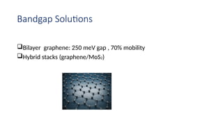
Propose bandgap engineering strategies for digital logic.
Develop a cost-scaling roadmap for industrial adoption.
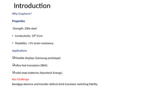
3. Introduction
Why Graphene?
Properties
Strength: 200x steel
• Conductivity: 10⁶ S/cm
• Flexibility: <1% strain resistance.
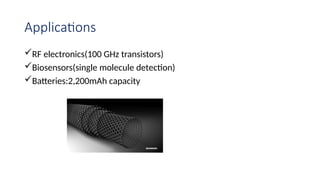
Applications
Flexible displays (Samsung prototype)
Ultra-fast transistors (IBM),
solid-state batteries (Nanotech Energy).
Key Challenge
Bandgap absence and transfer defects limit transistor switching fidelity.
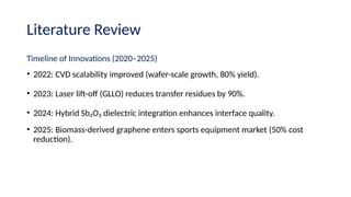
4. Literature Review
Timeline of Innovations (2020–2025)
• 2022: CVD scalability improved (wafer-scale growth, 80% yield).
• 2023: Laser lift-off (GLLO) reduces transfer residues by 90%.
• 2024: Hybrid Sb₂O₃ dielectric integration enhances interface quality.
• 2025: Biomass-derived graphene enters sports equipment market (50% cost
reduction).
5. 6. 7. Synthesis Techniques: Pros and Cons
Method ✅ Pros ❌ Cons
CVD Growth High purity, scalable Slow, expensive
Laser Lift-Off Low residue, thin films Precision alignment needed |
Biomass Conversion Eco-friendly, cheap Low conductivity |
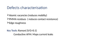
8. Why this Research Matters
Defect impact
• Simulation show 0.1% vacancies which implies 50% reduction in
mobility
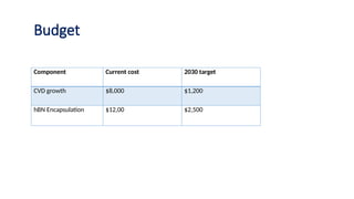
Cost projection
• Model 300mm wafer costs will drop to $500 2030 if CVD yield
improves by 65%
Thermal limit
• COMSOL analysis found graphene transistors overheat at 1mA/μm
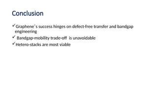
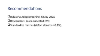
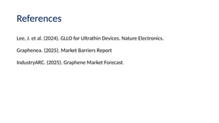
9. 10. 11. 12. 13. 14. 15. References
Lee, J. et al. (2024). GLLO for Ultrathin Devices. Nature Electronics.
Graphenea. (2025). Market Barriers Report
IndustryARC. (2025). Graphene Market Forecast.