Introduction to HFSS
A.Morales–Hernández
Department of Physics, Systems Engineering and Signal Theory
University Institute of Physics Applied to Sciences and Technologies
University of Alicante (SPAIN)
2.
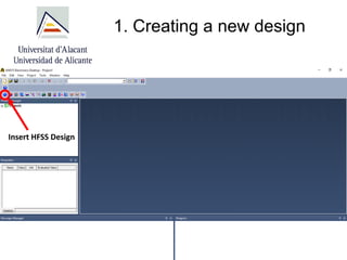
1. Creating anew design
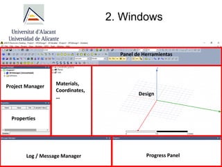
2. Windows
3. What do we want to desing?
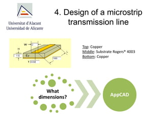
4. Design of a microstrip transmission line
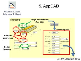
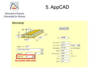
5. AppCAD
6. Design in HFSS
7. Design of a patch antenna
8. Other utilities of interest
Índice
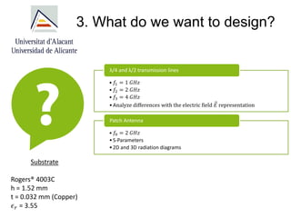
3. What dowe want to design?
• 𝑓1 = 1 𝐺𝐻𝑧
• 𝑓2 = 2 𝐺𝐻𝑧
• 𝑓3 = 4 𝐺𝐻𝑧
•Analyze differences with the electric field 𝐸 representation
λ/4 and λ/2 transmission lines
• 𝑓0 = 2 𝐺𝐻𝑧
•S-Parameters
•2D and 3D radiation diagrams
Patch Antenna
Substrate
Rogers® 4003C
h = 1.52 mm
t = 0.032 mm (Copper)
𝜖𝑟 = 3.55
6.
4. Design ofa microstrip
transmission line
Top: Copper
Middle: Substrate Rogers® 4003
Bottom: Copper
What
dimensions? AppCAD
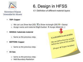
6. Design inHFSS
• TOP: Copper
o We can use Draw box (3D) o Draw rectangle (2D) + Sweep
o Assign name and material (Right button → Assign Material…)
• MIDDLE: Substrate material
o Same as the previous step.
• BOTTOM: Copper
o Same as the previous step.
• Air box
o Same as the previous step.
o Add Boundary Radiation
6.1 Definition of different material layers
10.
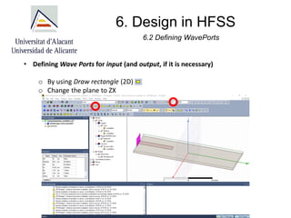
6. Design inHFSS
6.2 Defining WavePorts
• Defining Wave Ports for input (and output, if it is necessary)
o By using Draw rectangle (2D)
o Change the plane to ZX
11.
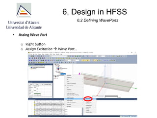
6. Design inHFSS
• Assing Wave Port
o Right button
o Assign Excitation → Wave Port…
6.2 Defining WavePorts
12.
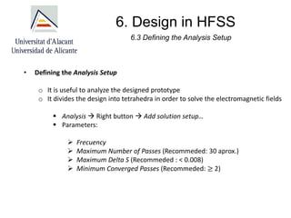
6. Design inHFSS
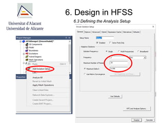
• Defining the Analysis Setup
o It is useful to analyze the designed prototype
o It divides the design into tetrahedra in order to solve the electromagnetic fields
▪ Analysis → Right button → Add solution setup…
▪ Parameters:
➢ Frecuency
➢ Maximum Number of Passes (Recommeded: 30 aprox.)
➢ Maximum Delta S (Recommeded : < 0.008)
➢ Minimum Converged Passes (Recommeded: ≥ 2)
6.3 Defining the Analysis Setup
6. Design inHFSS
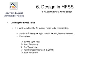
6.4 Defining the Sweep Setup
• Defining the Sweep Setup
o It is used to define the frequency range to be represented.
▪ Analysis → Setup → Right button → Add frequency sweep…
▪ Parameters:
➢ Sweep Type: Fast
➢ Start frequency
➢ End frequency
➢ Points (Recommended: ≥ 2000)
➢ Save Fields: No
6. Design inHFSS
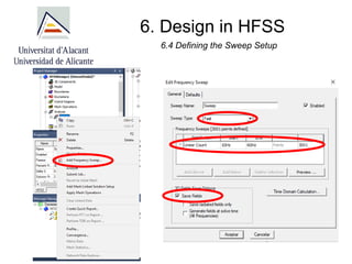
6.5 Validation Check
• Validation Check
o We can verify the design by using the button.
17.
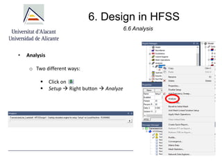
6. Design inHFSS
6.6 Analysis
• Analysis
o Two different ways:
▪ Click on
▪ Setup → Right button → Analyze
18.
6. Design inHFSS
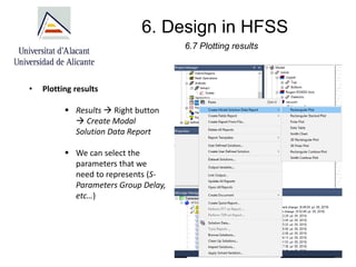
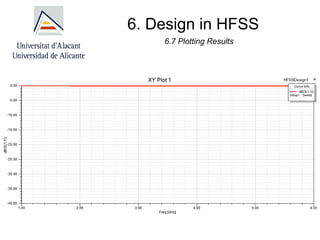
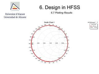
6.7 Plotting results
• Plotting results
▪ Results → Right button
→ Create Modal
Solution Data Report
▪ We can select the
parameters that we
need to represents (S-
Parameters Group Delay,
etc…)
6. Design inHFSS
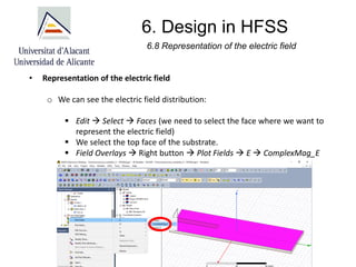
6.8 Representation of the electric field
• Representation of the electric field
o We can see the electric field distribution:
▪ Edit → Select → Faces (we need to select the face where we want to
represent the electric field)
▪ We select the top face of the substrate.
▪ Field Overlays → Right button → Plot Fields → E → ComplexMag_E
22.
6. Design inHFSS
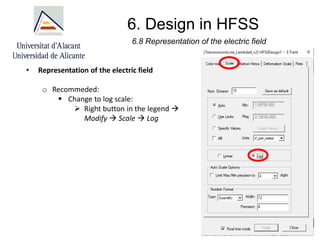
6.8 Representation of the electric field
• Representation of the electric field
o Recommeded:
▪ Change to log scale:
➢ Right button in the legend →
Modify → Scale → Log
23.
6. Design inHFSS
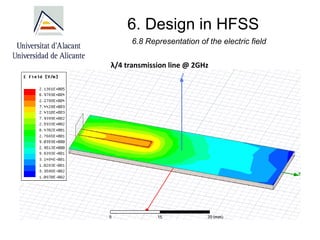
6.8 Representation of the electric field
λ/4 transmission line @ 2GHz
24.
6. Design inHFSS
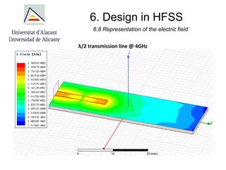
6.8 Representation of the electric field
λ/2 transmission line @ 4GHz
25.
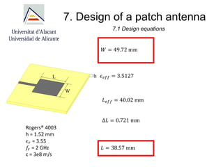
7. Design ofa patch antenna
7.1 Design equations
𝑊 =
𝑐
2 · 𝑓
𝑟
·
2
𝜖𝑟 + 1
𝜖𝑒𝑓𝑓 =
𝜖𝑟 + 1
2
+
𝜖𝑟 − 1
2
·
1
1 +
2 · ℎ
𝑊
𝐿𝑒𝑓𝑓 =
𝑐
2 · 𝑓
𝑟 · 𝜖𝑒𝑓𝑓
Δ𝐿 = 0.412 · ℎ ·
𝜖𝑒𝑓𝑓 + 0.3 ·
𝑊
ℎ
+ 0.264
𝜖𝑒𝑓𝑓 − 0.258 ·
𝑊
ℎ
+ 0.8
𝐿 = 𝐿𝑒𝑓𝑓 − 2 · Δ𝐿
[1] H. Werfelli, K. Tayari, M. Chaoui, M. Lahiani and
H. Ghariani, "Design of rectangular microstrip patch
antenna," 2016 2nd International Conference on
Advanced Technologies for Signal and Image
Processing (ATSIP), Monastir, 2016, pp. 798-803.
26.
7. Design ofa patch antenna
7.1 Design equations
𝑊 = 49.72 mm
𝜖𝑒𝑓𝑓 = 3.5127
𝐿𝑒𝑓𝑓 = 40.02 mm
Δ𝐿 = 0.721 mm
𝐿 = 38.57 mm
Rogers® 4003
h = 1.52 mm
𝜖𝑟 = 3.55
𝑓
𝑟 = 2 GHz
c = 3e8 m/s
27.
7. Design ofa patch antenna
7.2 Definition of layers and waveports
• Definition of layers
o Same steps as described in 6.1:
▪ Patch and input transmission line (“Unite”)
▪ Substrate
▪ Bottom copper layer
▪ Input waveport
▪ Air box and Boundary Radiation
28.
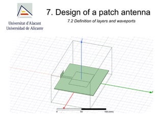
7. Design ofa patch antenna
7.2 Definition of layers and waveports
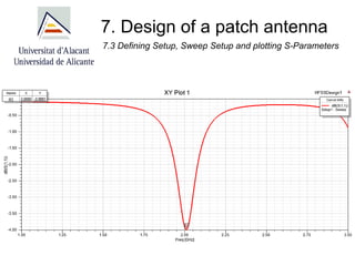
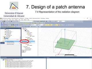
7. Design ofa patch antenna
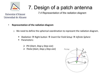
7.4 Representation of the radiation diagram
• Representation of the radiation diagram
o We need to define the spherical coordination to represent the radiation diagram.
▪ Radiation → Right button → Insert Far Field Setup → Infinite Sphere
▪ Parameters:
➢ Phi (Start, Stop y Step size)
➢ Theta (Start, Stop y Step size)
31.
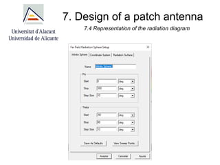
7. Design ofa patch antenna
7.4 Representation of the radiation diagram
32.
7. Design ofa patch antenna
7.4 Representation of the radiation diagram
33.
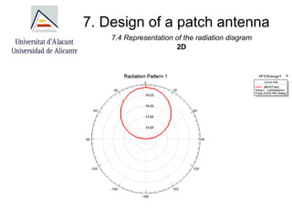
7. Design ofa patch antenna
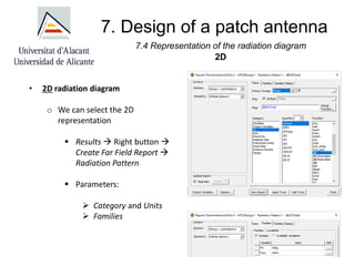
7.4 Representation of the radiation diagram
2D
• 2D radiation diagram
o We can select the 2D
representation
▪ Results → Right button →
Create Far Field Report →
Radiation Pattern
▪ Parameters:
➢ Category and Units
➢ Families
34.
7. Design ofa patch antenna
7.4 Representation of the radiation diagram
2D
35.
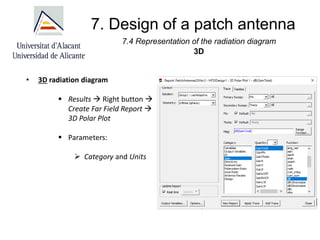
7. Design ofa patch antenna
7.4 Representation of the radiation diagram
3D
• 3D radiation diagram
▪ Results → Right button →
Create Far Field Report →
3D Polar Plot
▪ Parameters:
➢ Category and Units
36.
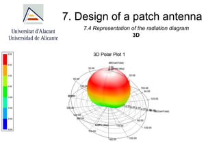
7. Design ofa patch antenna
7.4 Representation of the radiation diagram
3D
37.
8. Other utilitiesof interest
8.1 Edit Menu
• Edit menu on a circuit element
o Properties: Name, material, color, transparency,….
o Arrange: Move, rotate, duplicate, offset (1 element).
o Duplicate: Same as arrange for 2 or more elements.
o Scale: Increase or decrease the size by using a scale factor.
o Boolean: Unit, substract, intersect,…
o Sweep: To convert a 2D element into 3D.
38.
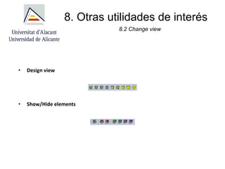
8. Otras utilidadesde interés
8.2 Change view
• Design view
• Show/Hide elements
39.
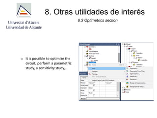
8. Otras utilidadesde interés
8.3 Optimetrics section
o It is possible to optimize the
circuit, perform a parametric
study, a sensitivity study,…

![7. Design of a patch antenna
7.1 Design equations
𝑊 =
𝑐
2 · 𝑓
𝑟
·
2
𝜖𝑟 + 1
𝜖𝑒𝑓𝑓 =
𝜖𝑟 + 1
2
+
𝜖𝑟 − 1
2
·
1
1 +
2 · ℎ
𝑊
𝐿𝑒𝑓𝑓 =
𝑐
2 · 𝑓
𝑟 · 𝜖𝑒𝑓𝑓
Δ𝐿 = 0.412 · ℎ ·
𝜖𝑒𝑓𝑓 + 0.3 ·
𝑊
ℎ
+ 0.264
𝜖𝑒𝑓𝑓 − 0.258 ·
𝑊
ℎ
+ 0.8
𝐿 = 𝐿𝑒𝑓𝑓 − 2 · Δ𝐿
[1] H. Werfelli, K. Tayari, M. Chaoui, M. Lahiani and
H. Ghariani, "Design of rectangular microstrip patch
antenna," 2016 2nd International Conference on
Advanced Technologies for Signal and Image
Processing (ATSIP), Monastir, 2016, pp. 798-803.](https://image.slidesharecdn.com/introductiontohfssmoraleshernandezaitor-250707201605-fe3aeef6/85/Introduction_to_HFSS_MoralesHernandezAitor-pdf-25-320.jpg)


![High_Frequency_Structure_Simulator_HFSS[1].pdf](https://cdn.slidesharecdn.com/ss_thumbnails/highfrequencystructuresimulatorhfss1-250707201635-2208bc58-thumbnail.jpg?width=640&height=640&fit=bounds)