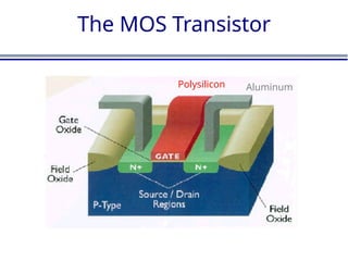
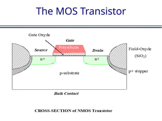
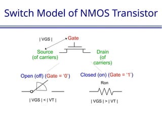
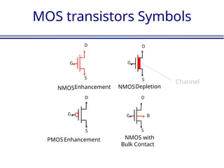
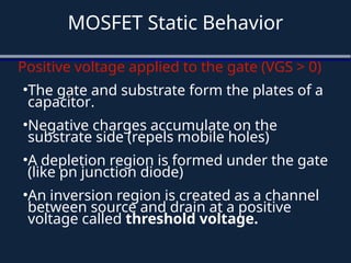
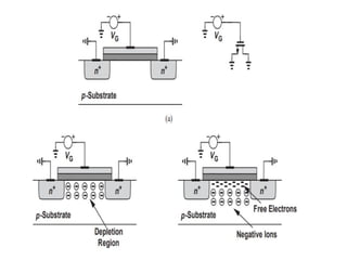
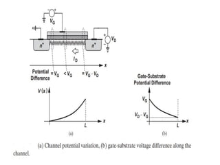
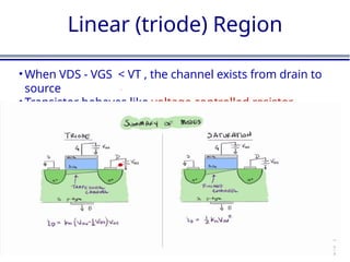
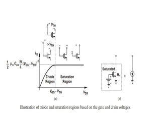
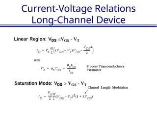
The Devices:
MOS Transistor
Karishma Parween
Government Engineering College,
Kishanganj
Learning Outcome
 Understand the basic structure and operation of
MOS devices.
 Analyze the I-V characteristics of MOS devices,
including the triode and saturation region.
 Calculate the threshold voltage , drain
current using mathematical models and
equations.
 Analyze the digital or switching models of MOS
transistor.
The MOS Transistor
Polysilicon Aluminum
The MOS Transistor
Switch Model of NMOS Transistor
Gate
Source
(of carriers)
Drain
(of
carriers)
| VGS |
| VGS | < | VT | | VGS | > | VT |
Open (off) (Gate = ‘0’) Closed (on) (Gate = ‘1’)
Ron
Switch Model of PMOS
Transistor
Gate
Source
(of carriers)
Drain
(of carriers)
| VGS |
Open (off) (Gate = ‘1’) Closed (on) (Gate = ‘0’)
Ron
MOS transistors Symbols
D
S
G
D
S
G
G
S
D D
S
G
NMOSEnhancement NMOS
PMOS
Depletion
Enhancement
B
NMOS with
Bulk Contact
Channel
MOSFET Static Behavior
Positive voltage applied to the gate (VGS > 0)
•The gate and substrate form the plates of a
capacitor.
•Negative charges accumulate on the
substrate side (repels mobile holes)
•A depletion region is formed under the gate
(like pn junction diode)
•An inversion region is created as a channel
between source and drain at a positive
voltage called threshold voltage.
Current-Voltage Relations
Assume VGS > VT
•A voltage difference VDS will cause ID to flow from
drain to source
•At a point x along the channel, the voltage is V(x),
and the gate-to-channel voltage is VGS - V(x)
•For channel to be present from drain to source, VGS
- V(x) > VT, i.e. VGS - VDS > VT for
channel to exist from drain to source
Linear (triode) Region
• When VDS - VGS < VT , the channel exists from drain to
source
• Transistor behaves like voltage controlled resistor
Saturation Region
• When VDS – VGS >= VT , the channel is pinched off
• Electrons are injected into depletion region and
accelerated towards drain by electric field
• Transistor behaves like voltage-controlled current source
Current-Voltage Relations
Long-Channel Device
THANK YOU!


Introduction to MOS DEVICE and it's structure.pptx

  • 1.
    The Devices: MOS Transistor KarishmaParween Government Engineering College, Kishanganj
  • 2.
    Learning Outcome  Understandthe basic structure and operation of MOS devices.  Analyze the I-V characteristics of MOS devices, including the triode and saturation region.  Calculate the threshold voltage , drain current using mathematical models and equations.  Analyze the digital or switching models of MOS transistor.
  • 3.
  • 4.
  • 5.
    Switch Model ofNMOS Transistor Gate Source (of carriers) Drain (of carriers) | VGS | | VGS | < | VT | | VGS | > | VT | Open (off) (Gate = ‘0’) Closed (on) (Gate = ‘1’) Ron
  • 6.
    Switch Model ofPMOS Transistor Gate Source (of carriers) Drain (of carriers) | VGS | Open (off) (Gate = ‘1’) Closed (on) (Gate = ‘0’) Ron
  • 7.
    MOS transistors Symbols D S G D S G G S DD S G NMOSEnhancement NMOS PMOS Depletion Enhancement B NMOS with Bulk Contact Channel
  • 8.
    MOSFET Static Behavior Positivevoltage applied to the gate (VGS > 0) •The gate and substrate form the plates of a capacitor. •Negative charges accumulate on the substrate side (repels mobile holes) •A depletion region is formed under the gate (like pn junction diode) •An inversion region is created as a channel between source and drain at a positive voltage called threshold voltage.
  • 10.
    Current-Voltage Relations Assume VGS> VT •A voltage difference VDS will cause ID to flow from drain to source •At a point x along the channel, the voltage is V(x), and the gate-to-channel voltage is VGS - V(x) •For channel to be present from drain to source, VGS - V(x) > VT, i.e. VGS - VDS > VT for channel to exist from drain to source
  • 12.
    Linear (triode) Region •When VDS - VGS < VT , the channel exists from drain to source • Transistor behaves like voltage controlled resistor
  • 13.
    Saturation Region • WhenVDS – VGS >= VT , the channel is pinched off • Electrons are injected into depletion region and accelerated towards drain by electric field • Transistor behaves like voltage-controlled current source
  • 15.
  • 16.

Editor's Notes

  • #4 The MOS transistor, or MOSFET is a very simple device to manufacture. It also lends itself to high scale integration. Several thousand devices can be manufactured on a single chip without the devices interacting with one another. Heavily doped n-type source and drain regions are implanted (diffused) into a lightly doped p-type substrate (body). A thin layer of SiO2 (gate oxide) is grown over the region between the source and drain and is covered by a polysilicon gate. Neighboring devices are shielded with a thick layer of SiO2 (field oxide) and a reverse-biased np-diode formed by adding a an extra P+ region (channel-stop implant or field implant) When a voltage larger than the threshold voltage, VT is applied to the gate, a conducting channel is formed between drain and source. Current can then flow from drain to source through the channel if there exists a potential difference between them. Current is carried by electrons in an NMOS transistor. This is unlike a diode where both electrons and holes carry the current though different types of material.
  • #5 Fourth terminal, body (bulk on previous slide)- substrate, not shown. Assumed connected to the appropriate supply rail, GND for NMOS, VDD for PMOS Electrons flow from source to drain – so current is referenced drain to source (IDS) Performs very well as a switch, little parasitic effects Today: STATIC (steady-state view) and later DYNAMIC (transient view) VGS < 0.43 V for off VGS > 0.43 V for on
  • #6 <number> <footer> <header> <date/time> holds flow source to drain – so current is referenced source to drain (ISD) VGS > 2.5 - .4 = 2.1 V for off and Vgs < 2.1 V for on
  • #7 MOS transistors can be either enhancement (no channel at VGS = 0) or depletion (finite channel at VGS = 0) types. Notice the thick line on the symbol that represents the channel. All MOSFET transistors actually have 4 pins (including the base [substrate] pin). Since the substrates are connected to the supply lines in digital circuits, they are typically not drawn.
  • #8 When a positive VGS is applied, the capacitor under the gate is charged with the gate having positive charges and the substrate (under the gate) having negative charges. The negative charges repel the mobile holes to form a depletion region under the gate.
  • #10 Now that a channel is formed from source to drain, a potential difference between them will cause current, ID to flow. However the difference of potential between source and drain, also affects the depth of the channel. So the difference between the gate and drain voltage must always be larger than the threshold voltage to maintain a channel from source to drain.
  • #12 So long as the the difference between the gate and drain voltage is larger than the threshold voltage, the channel will conduct current. It will have a finite resistance and behave like a voltage controlled resistor. Higher the gate voltage, lower the channel resistance.
  • #13 When the difference between the gate and drain voltage is less than the threshold voltage, the condition for the channels existence is no longer true near the drain region. The channel begins to pinch off, leaving a narrow depletion region near the drain. The charges will inject through the narrow depletion region and find its way to the drain since there is a large enough electric field to accelerate them. Therefore a small current will flow (saturation current). Under this (saturation) condition, the MOSFET behaves like a voltage-controlled current source.