Download to read offline

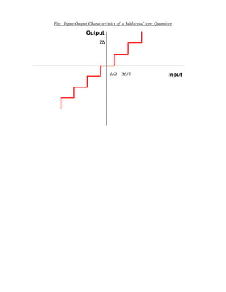
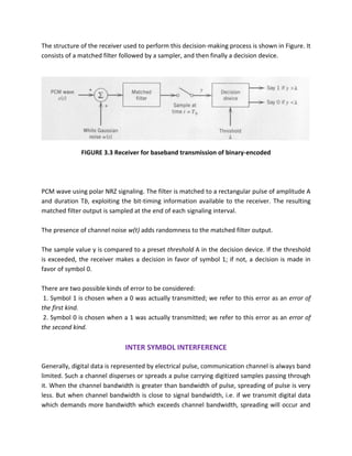
![QUANTIZATION NOISE AND SIGNAL-TO-NOISE:
“The Quantization process introduces an error defined as the difference between the
input signal, x(t) and the output signal, yt). This error is called the Quantization Noise.”
q(t) = x(t) – y(t)
Quantization noise is produced in the transmitter end of a PCM system by
rounding off sample values of an analog base-band signal to the nearest permissible
representation levels of the quantizer. As such quantization noise differs from channel
noise in that it is signal dependent.
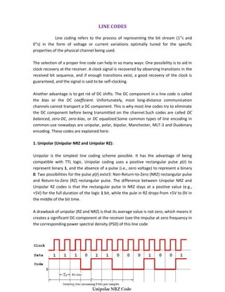
Let „Δ‟ be the step size of a quantizer and L be the total number of quantization levels.
Quantization levels are 0, ± ., ± 2 ., ±3 . . . . . . .
The Quantization error, Q is a random variable and will have its sample values bounded
by [-(Δ/2) < q < (Δ/2)]. If is small, the quantization error can be assumed to a uniformly
distributed random variable.
Consider a memory less quantizer that is both uniform and
symmetric. L = Number of quantization levels
X = Quantizer input
Y = Quantizer output
The output y is given by
Y=Q(x)
which is a staircase function that befits the type of mid tread or mid riser quantizer of
interest.
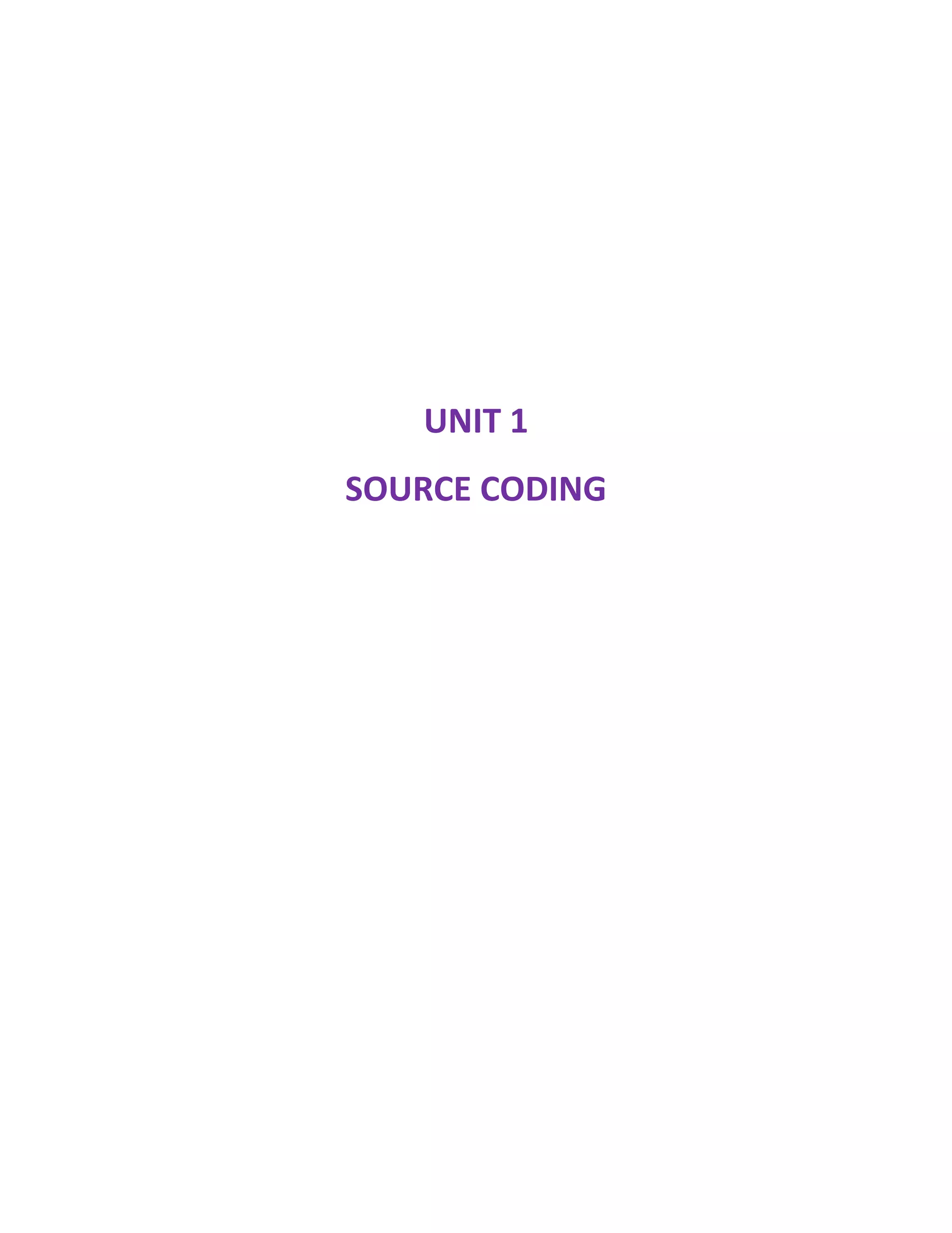
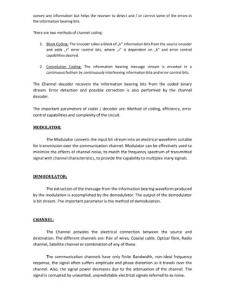
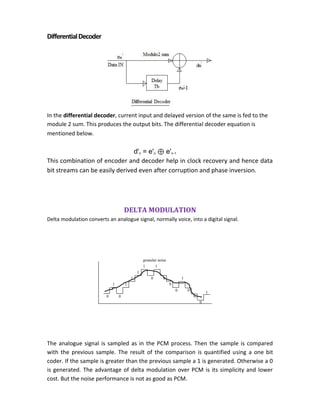
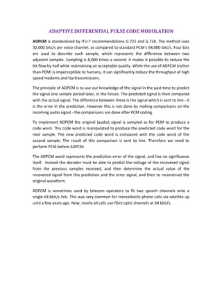
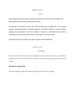
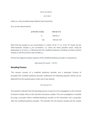
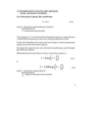
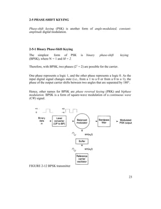
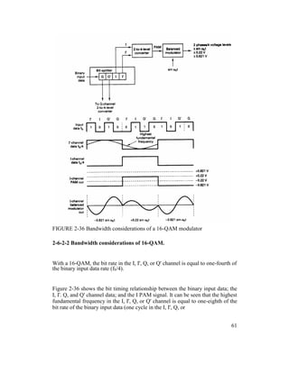
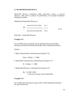
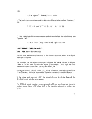
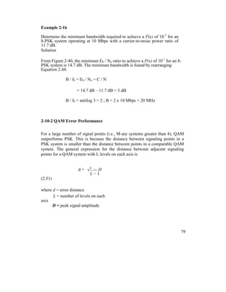
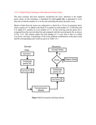
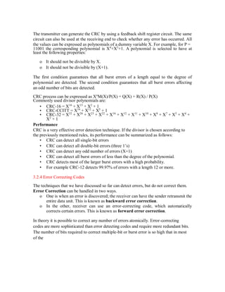
Non – Uniform Quantizer:
In Non – Uniform Quantizer the step size varies. The use of a non – uniform quantizer is
equivalent to passing the baseband signal through a compressor and then applying the
compressed signal to a uniform quantizer. The resultant signal is then transmitted.
UNIFORM
COMPRESSOR QUANTIZER EXPANDER
Fig: 2.14 MODEL OF NON UNIFORM QUANTIZER](https://image.slidesharecdn.com/ilovepdfmerged-180803062307/85/Ilovepdf-merged-10-320.jpg)
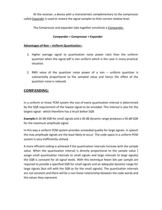
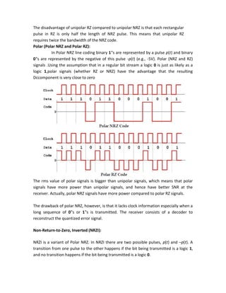
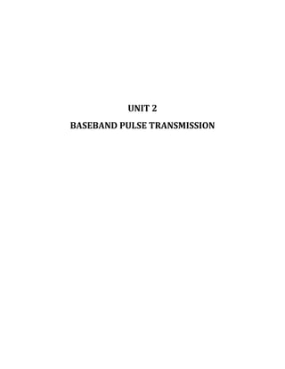
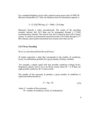
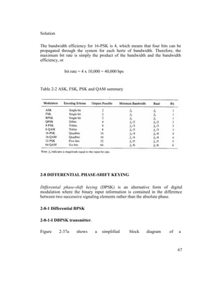
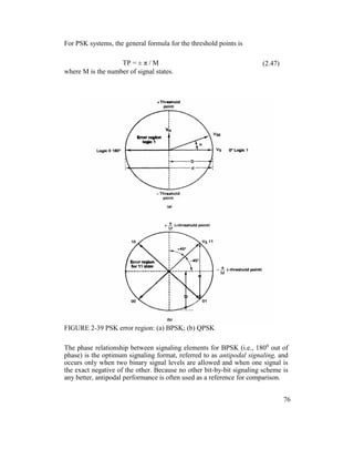
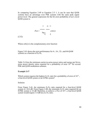
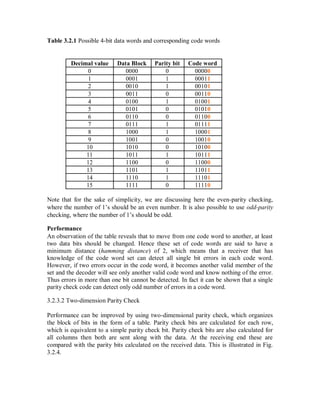
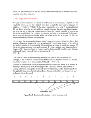
![DPCM is also designed to take advantage of the redundancies in a typical speech
waveform. In DPCM the differences between samples are quantized with fewer bits that
would be used for quantizing an individual amplitude sample. The sampling rate is often
the same as for a comparable PCM system, unlike Delta Modulation.
For the signals which does not change rapidly from one sample to next sample, the PCM
scheme is not preferred. When such highly correlated samples are encoded the
resulting encoded signal contains redundant information. By removing this redundancy
before encoding an efficient coded signal can be obtained. One of such scheme is the
DPCM technique. By knowing the past behavior of a signal up to a certain point in time,
it is possible to make some inference about the future values.
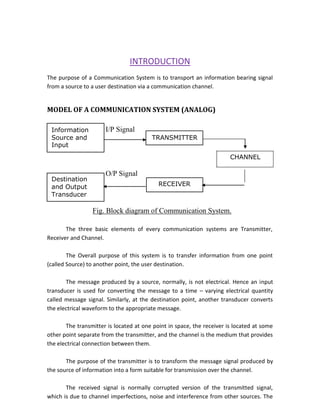
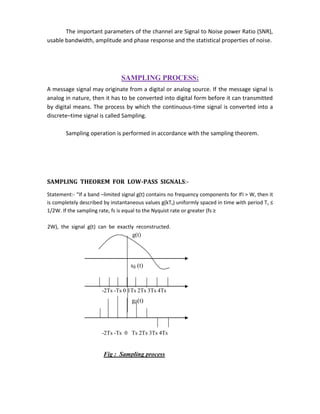
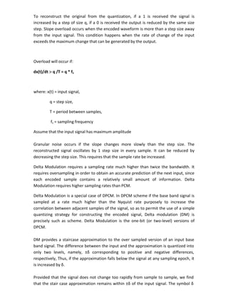
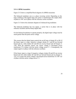
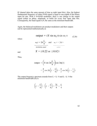
Transmitter: Let x(t) be the signal to be sampled and x(nTs) be it‟s samples. In this
scheme the input to the quantizer is a signal
e(nTs) = x(nTs) - x^(nTs)
where x^(nTs) is the prediction for unquantized sample x(nTs). This predicted value is
produced by using a predictor whose input, consists of a quantized versions of the input
signal x(nTs). The signal e(nTs) is called the prediction error.
By encoding the quantizer output, in this method, we obtain a modified version of the
PCM called differential pulse code modulation (DPCM).
Quantizer output, v(nTs) = Q[e(nTs)]
= e(nTs) + q(nTs)
where q(nTs) is the quantization error.
Predictor input is the sum of quantizer output and predictor output,
u(nTs) = x^(nTs) + e(nTs) + q(nTs)
u(nTs) = x(nTs) + q(nTs)
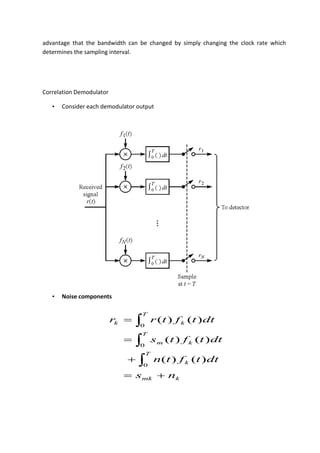
Accumulator
DAC
Quantiser
Enoder
ADC
Band Limiting
Filter +
-
Differentiator
Analogue
Input
Encoded
Difference
Samples](https://image.slidesharecdn.com/ilovepdfmerged-180803062307/85/Ilovepdf-merged-22-320.jpg)
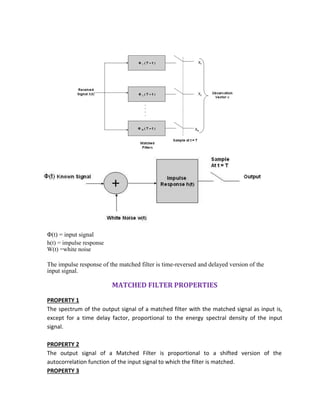
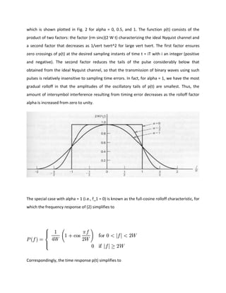
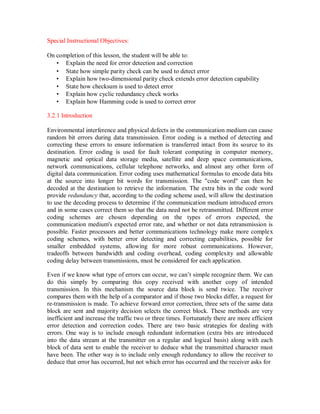
![INTRODUCTION
In signal processing, a matched filter is obtained by correlating a known signal, or template,
with an unknown signal to detect the presence of the template in the unknown signal.[1][2]
This
is equivalent to convolving the unknown signal with a conjugated time-reversed version of the
template. The matched filter is the optimal linear filter for maximizing the signal to noise ratio
(SNR) in the presence of additive stochastic noise. Matched filters are commonly used in radar,
in which a known signal is sent out, and the reflected signal is examined for common elements
of the out-going signal. Pulse compression is an example of matched filtering. It is so called
because impulse response is matched to input pulse signals. Two-dimensional matched filters
are commonly used in image processing, e.g., to improve SNR for X-ray. Matched filtering is a
demodulation technique with LTI (linear time invariant) filters to maximize SNR.[3]
It was
originally also known as a North filter.
MATCHED FILTER
Science each of t he orthonormal basic functions are Φ1(t) ,Φ2(t) …….ΦM(t) is assumed to
be zero outside the interval 0<t<T. we can design a linear filter with impulse response hj(t),
with the received signal x(t) the fitter output is given by the convolution integral
where xj is the j th
correlator output produced by the received signal x(t).
A filter whose impulse response is time-reversed and delayed version of the input signal is
said to be matched. Correspondingly , the optimum receiver based on this is referred as
the matched filter receiver.
For a matched filter operating in real time to be physically realizable, it must be causal. For
causal system](https://image.slidesharecdn.com/ilovepdfmerged-180803062307/85/Ilovepdf-merged-25-320.jpg)


![thus reducing tolerance for noise. The Nyquist theorem relates this time-domain condition to
an equivalent frequency-domain condition.
The Nyquist criterion is closely related to the Nyquist-Shannon sampling theorem, with only a
differing point of view.
This criterion can be intuitively understood in the following way: frequency-shifted replicas of
H(f) must add up to a constant value.
In practice this criterion is applied to baseband filtering by regarding the symbol sequence as
weighted impulses (Dirac delta function). When the baseband filters in the communication
system satisfy the Nyquist criterion, symbols can be transmitted over a channel with flat
response within a limited frequency band, without ISI. Examples of such baseband filters are
the raised-cosine filter, or the sinc filter as the ideal case.
Derivation
To derive the criterion, we first express the received signal in terms of the transmitted symbol
and the channel response. Let the function h(t) be the channel impulse response, x[n] the
symbols to be sent, with a symbol period of Ts; the received signal y(t) will be in the form
(where noise has been ignored for simplicity):
only one transmitted symbol has an effect on the received y[k] at sampling instants, thus
removing any ISI. This is the time-domain condition for an ISI-free channel. Now we find a
frequency-domain equivalent for it. We start by expressing this condition in continuous time:
This is the Nyquist ISI criterion and, if a channel response satisfies it, then there is no ISI
between the different samples.
RAISED COSINE SPECTRUM
We may overcome the practical difficulties encounted with the ideal Nyquist channel by
extending the bandwidth from the minimum value W = R_b/2 to an adjustable value between
W and 2 W. We now specify the frequency function P(f) to satisfy a condition more elaborate
than that for the ideal Nyquist channel; specifically, we retain three terms and restrict the
frequency band of interest to [-W, W], as shown by](https://image.slidesharecdn.com/ilovepdfmerged-180803062307/85/Ilovepdf-merged-31-320.jpg)
![that precedes the previous sample ( correlates these two samples) and the postcoder does the
reverse process.
The entire process of modified-duobinary decoding and the postcoding can be combined
together as one algorithm. The following decision rule is used for detecting the original
modified-duobinary signal samples {an} from {yn}
If yn<d, then a^n=0
If yn>d, then a^n=1
If yn=0, randomlyguess a^n
PARTIAL RESPONSE SIGNALLING
Partial response signalling (PRS), also known as correlative coding, was introduced for the first
time in 1960s for high data rate communication [lender, 1960]. From a practical point of view,
the background of this technique is related to the Nyquist criterion.
Assume a Pulse Amplitude Modulation (PAM), according to the Nyquist criterion, the highest
possible transmission rate without Inter-symbol-interference (ISI) at the receiver over a channel
with a bandwidth of W (Hz) is 2W symbols/sec.
BASEBAND M-ARY PAM TRANSMISSION
Up to now for binary systems the pulses have two possible amplitude levels. In a baseband M-
ary PAM system, the pulse amplitude modulator produces M possible amplitude levels with
M>2. In an M-ary system, the information source emits a sequence of symbols from an
alphabet that consists of M symbols. Each amplitude level at the PAM modulator output
corresponds to a distinct symbol. The symbol duration T is also called as the signaling rate of
the system, which is expressed as symbols per second or bauds.](https://image.slidesharecdn.com/ilovepdfmerged-180803062307/85/Ilovepdf-merged-40-320.jpg)


![CONVERSION OF CONTINUOUS AWGN CHANNEL INTO VECTOR CHANNEL
Perhaps the most important, and certainly the most analyzed, digital communication
channel is the AWGN channel shown in Figure.This channel passes the sum of the modulated
signal x(t) and an uncorrelated Gaussian noise n(t) to the output. The Gaussian noise is
assumed to be uncorrelated with itself (or “white”) for any non-zero time offset τ , that is
and zero mean, E[n(t)] = 0. With these definitions, the Gaussian noise is also strict sense
stationary). The analysis of the AWGN channel is a foundation for the analysis of more
complicated channel models in later chapters.
The assumption of white Gaussian noise is valid in the very common situation where the
noise is predominantly determined by front-end analog receiver thermal noise.](https://image.slidesharecdn.com/ilovepdfmerged-180803062307/85/Ilovepdf-merged-52-320.jpg)
![In the absence of additive noise in Figure y(t) = x(t), and the demodulation process would
exactly recover the transmitted signal. This section shows that for the AWGN channel, this
demodulation process provides sufficient information to determine optimally the transmit-
ted signal. The resulting components i, l = 1, ..., N comprise a vector channel
output, y = [y1 , ..., yN ]0
that is equivalent for detection purposes to y(t). The analysis can
thus convert the continuous channel y(t) = x(t) + n(t) to a discrete vector channel model,
y = x + n ,
where n = [n1 n2 ... nN ] and nl = hn(t), ϕl(t)i. The vector channel output is the sum of the
vector equivalent of the modulated signal and the vector equivalent of the demodulated
noise. Nevertheless, the exact noise sample function may not be reconstructed from n,
There may exist a component of n(t) that is orthogonal to the space spanned by the basis
functions {ϕ1(t) ... ϕN (t)}. This unrepresented noise component is
n˜(t) = n(t) − nˆ(t) = y(t) − yˆ(t) .
The development of the MAP detector could have replaced y by y(t) everywhere and the
development would have proceeded identically with the tacit inclusion of the time variable t
in the probability densities (and also assuming stationarity of y(t) as a random process). The
Theorem of Irrelevance would hold with [y1 y2] replaced by [ˆy(t) ˜n(s)], as long as the
relation holds for any pair of time instants t and s. In a non-mathematical sense, the
unrepresented noise is useless to the receiver, so there is nothing of value lost in the vector
demodulator, even though some of the channel output noise is not represented.
The following algebra demonstrates that ˜n(s) is irrelevant:
First,](https://image.slidesharecdn.com/ilovepdfmerged-180803062307/85/Ilovepdf-merged-53-320.jpg)
![Correlator outputs
km
kmN
dtftfN
ddtftfntnEnnE
T
mk
T T
mkmk
0
2
1
)()(
2
1
)()()]()([)(
0
0
0
0 0
EQIVALANCE OF CORRELATION N MATCHED FILTER RECEIVER
• Use filters whose impulse response is the orthonormal basis of signal
• Can show this is exactly equivalent to the
correlation demodulator
• We find that this Demodulator Maximizes the SNR
• Essentially show that any other function than f1() decreases SNR as is not as well
correlated to components of r(t)](https://image.slidesharecdn.com/ilovepdfmerged-180803062307/85/Ilovepdf-merged-58-320.jpg)


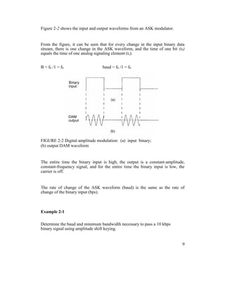
![Mathematically, amplitude-shift keying is
(2.12)
where
vask(t) = amplitude-shift keying wave
vm(t) = digital information (modulating) signal (volts) A/2 =
unmodulated carrier amplitude (volts)
ωc = analog carrier radian frequency (radians per second, 2πfct)
In Equation 2.12, the modulating signal [vm(t)] is a normalized binary
waveform, where + 1 V = logic 1 and -1 V = logic 0. Therefore, for a logic 1
input, vm(t) = + 1 V, Equation 2.12 reduces to
and for a logic 0 input, vm(t) = -1 V, Equation 2.12 reduces to
Thus, the modulated wave vask(t), is either A cos(ωc t) or 0. Hence, the carrier is
either "on"or "off," which is why amplitude-shift keying is sometimes referred to
as on-off keying(OOK).
8](https://image.slidesharecdn.com/ilovepdfmerged-180803062307/85/Ilovepdf-merged-71-320.jpg)
![(hertz)
vm(t) = binary input (modulating) signal (volts)
From Equation 2.13, it can be seen that the peak shift in the carrier frequency ( f)
is proportional to the amplitude of the binary input signal (vm[t]), and the
direction of the shift is determined by the polarity.
The modulating signal is a normalized binary waveform where a logic 1 = + 1 V
and a logic 0 = -1 V. Thus, for a logic l input, vm(t) = + 1, Equation 2.13 can be
rewritten as
For a logic 0 input, vm(t) = -1, Equation 2.13 becomes
With binary FSK, the carrier center frequency (fc) is shifted (deviated) up and
down in the frequency domain by the binary input signal as shown in Figure 2-
3.
FIGURE 2-3 FSK in the frequency domain
11](https://image.slidesharecdn.com/ilovepdfmerged-180803062307/85/Ilovepdf-merged-74-320.jpg)
![comparator follows the frequency shift.
Because there are only two input frequencies (mark and space), there are also
only two output error voltages. One represents a logic 1 and the other a logic 0.
Binary FSK has a poorer error performance than PSK or QAM and,
consequently, is seldom used for high-performance digital radio systems.
Its use is restricted to low-performance, low-cost, asynchronous data modems
that are used for data communications over analog, voice-band telephone lines.
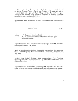
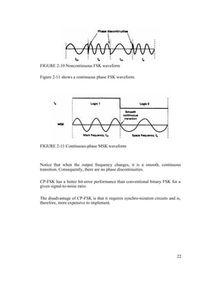
2-4-4 Continuous-Phase Frequency-Shift Keying
Continuous-phase frequency-shift keying (CP-FSK) is binary FSK except the
mark and space frequencies are synchronized with the input binary bit rate.
With CP-FSK, the mark and space frequencies are selected such that they are
separated from the center frequency by an exact multiple of one-half the bit rate
(fm and fs = n[fb / 2]), where n = any integer).
This ensures a smooth phase transition in the analog output signal when it
changes from a mark to a space frequency or vice versa.
Figure 2-10 shows a noncontinuous FSK waveform. It can be seen that when the
input changes from a logic 1 to a logic 0 and vice versa, there is an abrupt phase
discontinuity in the analog signal. When this occurs, the demodulator has trouble
following the frequency shift; consequently, an error may occur.
21](https://image.slidesharecdn.com/ilovepdfmerged-180803062307/85/Ilovepdf-merged-84-320.jpg)
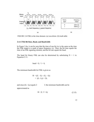
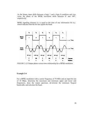
![Each time the input logic condition changes, the output phase changes.
Mathematically, the output of a BPSK modulator is proportional to
BPSK output = [sin (2πfat)] x [sin (2πfct)] (2.20)
where
fa = maximum fundamental frequency of binary input (hertz)
fc = reference carrier frequency (hertz)
Solving for the trig identity for the product of two sine functions,
0.5cos[2π(fc – fa)t] – 0.5cos[2π(fc + fa)t]
Thus, the minimum double-sided Nyquist bandwidth (B) is
fc + fa fc + fa
-(fc + fa) or -fc
+ f
a
2fa
and because fa = fb / 2, where fb = input bit rate,
where B is the minimum double-sided Nyquist bandwidth.
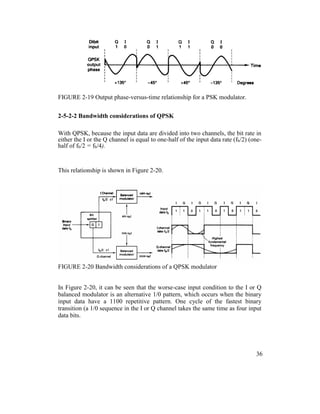
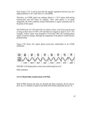
Figure 2-15 shows the output phase-versus-time relationship for a BPSK
waveform.
Logic 1 input produces an analog output signal with a 0° phase angle, and a
logic 0 input produces an analog output signal with a 180° phase angle.
27](https://image.slidesharecdn.com/ilovepdfmerged-180803062307/85/Ilovepdf-merged-90-320.jpg)
![Solution
Substituting into Equation 2-20 yields
output = [sin (2πfat)] x [sin (2πfct)] ; fa = fb / 2 = 5 MHz
= [sin 2π(5MHz)t)] x [sin 2π(70MHz)t)]
= 0.5cos[2π(70MHz – 5MHz)t] – 0.5cos[2π(70MHz + 5MHz)t]
lower side frequency upper side frequency
Minimum lower side frequency (LSF):
LSF=70MHz - 5MHz = 65MHz
Maximum upper side frequency (USF):
USF = 70 MHz + 5 MHz = 75 MHz
Therefore, the output spectrum for the worst-case binary input conditions is
as follows: The minimum Nyquist bandwidth (B) is
B = 75 MHz - 65 MHz = 10 MHz
and the baud = fb or 10 megabaud.
29](https://image.slidesharecdn.com/ilovepdfmerged-180803062307/85/Ilovepdf-merged-92-320.jpg)
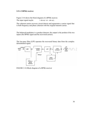
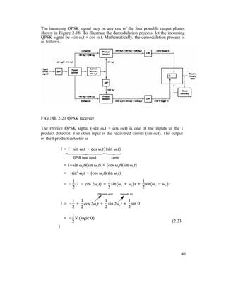
![Mathematically, the demodulation process is as follows.
For a BPSK input signal of + sin ωct (logic 1), the output of the balanced
modulator is
output = (sin ωct )(sin ωct) = sin2
ωct (2.21)
or
sin2
ωct = 0.5(1 – cos 2ωct) = 0.5 - 0.5cos 2ωct
filtered out
leaving
output = + 0.5 V = logic 1
It can be seen that the output of the balanced modulator contains a positive
voltage (+[1/2]V) and a cosine wave at twice the carrier frequency (2 ωct ).
The LPF has a cutoff frequency much lower than 2 ωct, and, thus, blocks the
second harmonic of the carrier and passes only the positive constant component.
A positive voltage represents a demodulated logic 1.
For a BPSK input signal of -sin ωct (logic 0), the output of the balanced
modulator is
output = (-sin ωct )(sin ωct) = sin2
ωct
or
sin2
ωct = -0.5(1 – cos 2ωct) = 0.5 + 0.5cos 2ωct
filtered out
31](https://image.slidesharecdn.com/ilovepdfmerged-180803062307/85/Ilovepdf-merged-94-320.jpg)
![leaving
output = - 0.5 V = logic 0
The output of the balanced modulator contains a negative voltage (-[l/2]V) and a
cosine wave at twice the carrier frequency (2ωct).
Again, the LPF blocks the second harmonic of the carrier and passes only the
negative constant component. A negative voltage represents a demodulated logic
0.
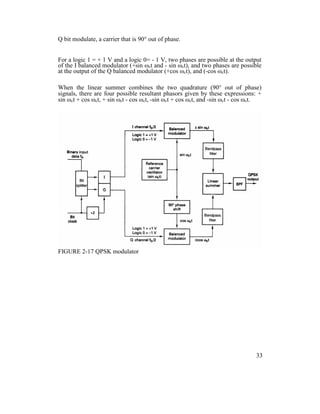
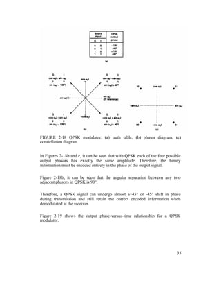
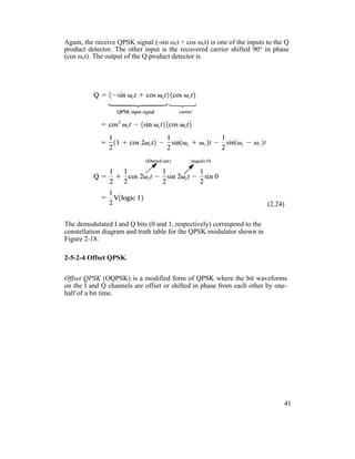
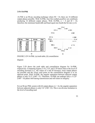
2-5-2 Quaternary Phase-Shift Keying
QPSK is an M-ary encoding scheme where N = 2 and M= 4 (hence, the name
"quaternary" meaning "4"). A QPSK modulator is a binary (base 2) signal, to
produce four different input combinations,: 00, 01, 10, and 11.
Therefore, with QPSK, the binary input data are combined into groups of two
bits, called dibits. In the modulator, each dibit code generates one of the four
possible output phases (+45°, +135°, -45°, and -135°).
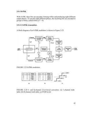
2-5-2-1 QPSK transmitter.
A block diagram of a QPSK modulator is shown in Figure 2-17. Two bits (a
dibit) are clocked into the bit splitter. After both bits have been serially inputted,
they are simultaneously parallel outputted.
The I bit modulates a carrier that is in phase with the reference oscillator (hence
the name "I" for "in phase" channel), and the
32](https://image.slidesharecdn.com/ilovepdfmerged-180803062307/85/Ilovepdf-merged-95-320.jpg)


![Example 2-4. Use the QPSK block diagram shown in Figure 2-17 as the
modulator model.
Solution
The bit rate in both the I and Q channels is equal to one-half of the
transmission bit rate, or
fbQ = fb1 = fb / 2 = 10 Mbps / 2 = 5 Mbps
The highest fundamental frequency presented to either balanced modulator
is
fa= fbQ / 2 = 5 Mbps / 2 = 2.5 MHz
The output wave from each balanced modulator is (sin
2πfat)(sin 2πfct)
0.5 cos 2π(fc – fa)t – 0.5 cos 2π(fc + fa)t
0.5 cos 2π[(70 – 2.5)MHz]t – 0.5 cos 2π[(70 –
2.5)MHz]t
0.5 cos 2π(67.5MHz)t - 0.5 cos 2π(72.5MHz)t
The minimum Nyquist bandwidth is
B=(72.5-67.5)MHz = 5MHz
The symbol rate equals the bandwidth: thus,
symbol rate = 5 megabaud
38](https://image.slidesharecdn.com/ilovepdfmerged-180803062307/85/Ilovepdf-merged-101-320.jpg)

![Mathematically, the output of the balanced modulators is
The output frequency spectrum extends from fc + fb / 6 to fc - fb / 6, and the
minimum bandwidth (fN) is
Example 2-8
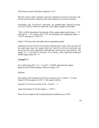
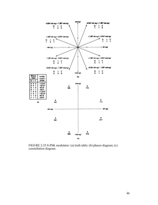
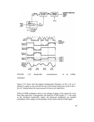
For an 8-PSK modulator with an input data rate (fb) equal to 10 Mbps and a
carrier frequency of 70 MHz, determine the minimum double-sided Nyquist
bandwidth (fN) and the baud. Also, compare the results with those achieved with
the BPSK and QPSK modulators in Examples 2-4 and 2-6. If the 8-PSK block
diagram shown in Figure 2-23 as the modulator model.
Solution
The bit rate in the I, Q, and C channels is equal to one-third of the input bit rate,
or 10 Mbps
fbc = fbQ = fb1 = 10 Mbps / 3 = 3.33 Mbps
Therefore, the fastest rate of change and highest fundamental frequency
presented to either balanced modulator is
fa = fbc / 2 = 3.33 Mbps / 2 = 1.667 Mbps
The output wave from the balance modulators is (sin
2πfat)(sin 2πfct)
0.5 cos 2π(fc – fa)t – 0.5 cos 2π(fc + fa)t
0.5 cos 2π[(70 – 1.667)MHz]t – 0.5 cos 2π[(70
50](https://image.slidesharecdn.com/ilovepdfmerged-180803062307/85/Ilovepdf-merged-113-320.jpg)
![+ 1.667)MHz]t
0.5 cos 2π(68.333MHz)t - 0.5 cos
2π(71.667MHz)t
The minimum Nyquist bandwidth is
B= (71.667 - 68.333) MHz = 3.333 MHz
The minimum bandwidth for the 8-PSK can also be determined by simply
substituting into Equation 2-10:
B = 10 Mbps / 3 = 3.33 MHz
Again, the baud equals the bandwidth; thus, baud =
3.333 megabaud
The output spectrum is as follows:
B = 3.333 MHz
It can be seen that for the same input bit rate the minimum bandwidth required to
pass the output of an 8-PSK modulator is equal to one-third that of the BPSK
modulator in Example 2-4 and 50% less than that required for the QPSK
modulator in Example 2-6. Also, in each case the baud has been reduced by the
same proportions.
51](https://image.slidesharecdn.com/ilovepdfmerged-180803062307/85/Ilovepdf-merged-114-320.jpg)
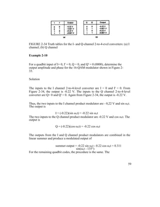
![Example 2 -11
For a 16-QAM modulator with an input data rate (fb) equal to 10 Mbps and a
carrier frequency of 70 MHz, determine the minimum double-sided Nyquist
frequency (fN) and the baud. Also, compare the results with those achieved with
the BPSK, QPSK, and 8-PSK modulators in Examples 2-4, 2-6, and 2-8. Use the
16-QAM block diagram shown in Figure 2-33 as the modulator model.
Solution
The bit rate in the I, I’, Q, and Q’ channels is equal to one-fourth of the input bit
rate,
fbI = fbI’ = fbQ = fbQ’ = fb / 4 = 10 Mbps / 4 = 2.5
Mbps
Therefore, the fastest rate of change and highest fundamental frequency
presented to either balanced modulator is
fa = fbI / 2 = 2.5 Mbps / 2 = 1.25 MHz The
output wave from the balanced modulator is
(sin 2πfat)(sin 2πfct)
0.5 cos 2π(fc – fa)t – 0.5 cos 2π(fc + fa)t
0.5 cos 2π[(70 – 1.25)MHz]t – 0.5 cos 2π[(70 +
1.25)MHz]t
0.5 cos 2π(68.75MHz)t - 0.5 cos
2π(71.25MHz)t
The minimum Nyquist bandwidth is
63](https://image.slidesharecdn.com/ilovepdfmerged-180803062307/85/Ilovepdf-merged-126-320.jpg)


![100,000 bits transmitted.
Probability of error is a function of the carrier-to-noise power ratio (or, more
specifically, the average energy per bit-to-noise power density ratio) and the
number of possible encoding conditions used (M-ary).
Carrier-to-noise power ratio is the ratio of the average carrier power (the
combined power of the carrier and its associated sidebands) to the thermal noise
power Carrier power can be stated in watts or dBm. where
C(dBm) = 10 log [C(watts) / 0.001] (2.28)
Thermal noise power is expressed mathematically as
N = KTB (watts) (2.29)
where
N = thermal noise power (watts)
K = Boltzmann's proportionality constant (1.38 X 10⁻²³
joules per kelvin)
T= temperature (kelvin: 0 K=-273° C, room temperature = 290 K)
B = bandwidth (hertz)
Stated in dBm, N(dBm) = 10 log [KTB / 0.001] (2.30)
Mathematically, the carrier-to-noise power ratio is
C / N = C / KTB (unitless ratio) (2.31)
where
C = carrier power (watts)
N = noise power (watts)
71](https://image.slidesharecdn.com/ilovepdfmerged-180803062307/85/Ilovepdf-merged-134-320.jpg)
![Stated in dB, C / N (dB) = 10 log [C / N]
= C
(dBm) – N
(dBm) (2.32)
Energy per bit is simply the energy of a single bit of information.
Mathematically, energy per bit is
Eb = CTb (J/bit) (2.33)
where
Eb = energy of a single bit (joules per bit)
Tb = time of a single bit (seconds) C =
carrier power (watts)
Stated in dBJ, Eb(dBJ) = 10 log Eb (2.34)
and because Tb = 1/fb, where fb is the bit rate in bits per second, Eb can be
rewritten as
Eb = C / fb (J/bit) (2.35)
Stated in dBJ, Eb(dBJ) = 10 log C / fb (2.36)
= 10 log C – 10 log fb (2.37)
Noise power density is the thermal noise power normalized to a 1-Hz bandwidth
(i.e., the noise power present in a 1-Hz bandwidth). Mathematically, noise power
density is
No = N / B (W/Hz) (2.38)
where
72](https://image.slidesharecdn.com/ilovepdfmerged-180803062307/85/Ilovepdf-merged-135-320.jpg)
![= 10 log Eb - 10 log No (2.46)
Example 2-15
For a QPSK system and the given parameters, determine
a. Carrier power in dBm.
b. Noise power in dBm.
c. Noise power density in dBm.
d. Energy per bit in dBJ.
e. Carrier-to-noise power ratio in dB.
f.. EblNo ratio.
C = 10-12
W
Fb = 60 kbps
N = 1.2 x 10 -14
W
B = 120 kHz
Solution
a. The carrier power in dBm is determined by substituting into Equation 2.28:
C = 10 log (10 -12
/ 0.001) = - 90 dBm
b. The noise power in dBm is determined by substituting into Equation 2-30:
N = 10 log [(1.2x10⁻¹⁴
) / 0.001] = -109.2 dBm
c. The noise power density is determined by substituting into Equation 2-40:
No = -109.2 dBm – 10 log 120 kHz = -160 dBm
d. The energy per bit is determined by substituting into equation
74](https://image.slidesharecdn.com/ilovepdfmerged-180803062307/85/Ilovepdf-merged-137-320.jpg)


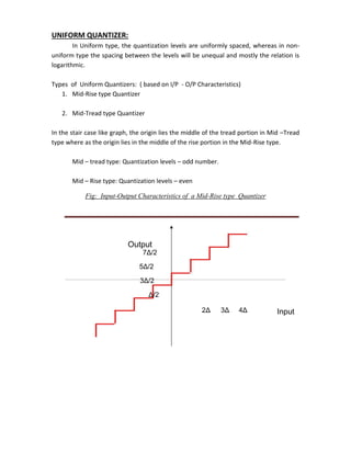
![Figure : An example of a convolutional code with two parity bits per message bit (r
= 2) and constraint length (shown in the rectangular window) K = 3.
while providing a low enough resulting probability of a bit error.
In 6.02, we will use K (upper case) to refer to the constraint length, a somewhat un-
fortunate choice because we have used k (lower case) in previous lectures to refer to the
number of message bits that get encoded to produce coded bits. Although “L” might be a
better way to refer to the constraint length, we’ll use K because many papers and docu-
ments in the field use K (in fact, most use k in lower case, which is especially confusing).
Because we will rarely refer to a “block” of size k while talking about convolutional
codes, we hope that this notation won’t cause confusion.
Armed with this notation, we can describe the encoding process succinctly. The
encoder looks at K bits at a time and produces r parity bits according to carefully chosen
functions that operate over various subsets of the K bits.1
One example is shown in
Figure 8-1, which shows a scheme with K = 3 and r = 2 (the rate of this code, 1/r = 1/2).
The encoder spits out r bits, which are sent sequentially, slides the window by 1 to the
right, and then repeats the process. That’s essentially it.
At the transmitter, the only remaining details that we have to worry about now are:
• What are good parity functions and how can we represent them conveniently?
• How can we implement the encoder efficiently?
The rest of this lecture will discuss these issues, and also explain why these codes are
called “convolutional”.
Parity Equations
The example in Figure 8-1 shows one example of a set of parity equations, which govern
the way in which parity bits are produced from the sequence of message bits, X. In this
example, the equations are as follows (all additions are in F2)):
p0[n] = x[n] + x[n − 1] + x[n − 2]
(8.1)p1[n] = x[n] + x[n − 1]](https://image.slidesharecdn.com/ilovepdfmerged-180803062307/85/Ilovepdf-merged-176-320.jpg)
![By convention, we will assume that each message has K − 1 “0” bits padded in front,
so that the initial conditions work out properly.
An example of parity equations for a rate 1/3 code is
p0[n] = x[n] + x[n − 1] + x[n − 2]
p1[n] = x[n] + x[n − 1]
(8.2)p2[n] = x[n] + x[n − 2]
In general, one can view each parity equation as being produced by composing the
mes-sage bits, X, and a generator polynomial, g. In the first example above, the
generator poly-nomial coefficients are (1, 1, 1) and (1, 1, 0), while in the second, they are
(1, 1, 1), (1, 1, 0), and (1, 0, 1).
We denote by gi the K-element generator polynomial for parity bit pi. We can then
write pi as follows:
k−1
j
pi[n] = ( gi[j]x[n − j]) mod 2. (8.3)
=0
The form of the above equation is a convolution of g and x—hence the term “convolu-
tional code”. The number of generator polynomials is equal to the number of generated
parity bits, r, in each sliding window.
8.2.1 An Example
Let’s consider the two generator polynomials of Equations 8.1 (Figure 8-1). Here, the
gen-erator polynomials are
g0 = 1, 1, 1
g1 = 1, 1, 0
(8.4)
If the message sequence, X = [1, 0, 1, 1, . . .] (as usual, x[n] = 0 ∀n < 0), then the
parity bits from Equations 8.1 work out to be
p0[0] = (1 + 0 + 0) = 1
p1[0] = (1 + 0)= 1
p0[1] = (0 + 1 + 0) = 1
p1[1] = (0 + 1)= 1
p0[2] = (1 + 0 + 1) = 0
p1[2] = (1 + 0)= 1
p0[3] = (1 + 1 + 0) = 0](https://image.slidesharecdn.com/ilovepdfmerged-180803062307/85/Ilovepdf-merged-177-320.jpg)
![p1[3] = (1 + 1)= 0. (8.5)
Therefore, the parity bits sent over the channel are [1, 1, 1, 1, 0, 0, 0, 0, . . .].
There are several generator polynomials, but understanding how to construct good
ones is outside the scope of 6.02. Some examples (found by J. Busgang) are shown in
Table 8-1.
Constraint length G1 G2
3 110 111
4 1101 1110
5 11010 11101
6 110101 111011
7 110101 110101
8 110111 1110011
9 110111 111001101
10 110111001 1110011001
Table : Examples of generator polynomials for rate 1/2 convolutional codes with
different constraint lengths.
Figure 8-2: Block diagram view of convolutional coding with shift
registers.
8.3 Two Views of the Convolutional Encoder
We now describe two views of the convolutional encoder, which we will find useful in
better understanding convolutional codes and in implementing the encoding and decod-
ing procedures. The first view is in terms of a block diagram, where one can construct
the mechanism using shift registers that are connected together. The second is in terms of
a state machine, which corresponds to a view of the encoder as a set of states with well-
defined transitions between them. The state machine view will turn out to be extremely
useful in figuring out how to decode a set of parity bits to reconstruct the original
message bits.](https://image.slidesharecdn.com/ilovepdfmerged-180803062307/85/Ilovepdf-merged-178-320.jpg)
![Block Diagram View
Figure 8-2 shows the same encoder as Figure 8-1 and Equations (8.1) in the form of a
block diagram. The x[n − i] values (here there are two) are referred to as the state of the
encoder. The way to think of this block diagram is as a “black box” that takes message
bits in and spits out parity bits.
Input message bits, x[n], arrive on the wire from the left. The box calculates the parity
bits using the incoming bits and the state of the encoder (the k − 1 previous bits; 2 in this
example). After the r parity bits are produced, the state of the encoder shifts by 1, with
x[n]
Figure 8-3: State machine view of convolutional coding.
taking the place of x[n − 1], x[n − 1] taking the place of x[n − 2], and so on, with x[n − K
+ 1] being discarded. This block diagram is directly amenable to a hardware
implementation using shift registers.
State Machine View
Another useful view of convolutional codes is as a state machine, which is shown in Fig-
ure 8-3 for the same example that we have used throughout this lecture (Figure 8-1).
The state machine for a convolutional code is identical for all codes with a given con-
straint length, K, and the number of states is always 2K−1
. Only the pi labels change de-
pending on the number of generator polynomials and the values of their coefficients.
Each](https://image.slidesharecdn.com/ilovepdfmerged-180803062307/85/Ilovepdf-merged-179-320.jpg)
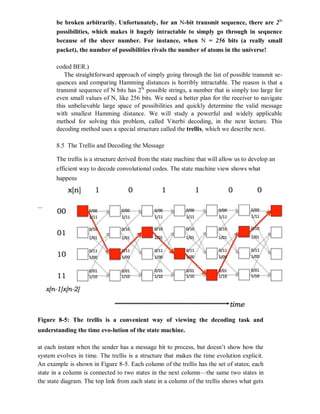
![state is labeled with x[n − 1]x[n − 2] . . . x[n − K + 1]. Each arc is labeled with x[n]/p0p1 .
. ..
In this example, if the message is 101100, the transmitted bits are 11 11 01 00 01 10.
This state machine view is an elegant way to explain what the transmitter does, and
also what the receiver ought to do to decode the message, as we now explain. The
transmitter begins in the initial state (labeled “STARTING STATE” in Figure 8-3) and
processes the message one bit at a time. For each message bit, it makes the state transition
from the current state to the new one depending on the value of the input bit, and sends
the parity bits that are on the corresponding arc.
The receiver, of course, does not have direct knowledge of the transmitter’s state
transi-tions. It only sees the received sequence of parity bits, with possible corruptions.
Its task is to determine the best possible sequence of transmitter states that could have
produced the parity bit sequence. This task is called decoding, which we will introduce
next, and then study in more detail in the next lecture.
8.4 The Decoding Problem
As mentioned above, the receiver should determine the “best possible” sequence of trans-
mitter states. There are many ways of defining “best”, but one that is especially appealing
is the most likely sequence of states (i.e., message bits) that must have been traversed
(sent) by the transmitter. A decoder that is able to infer the most likely sequence is also
called a maximum likelihood decoder.
Consider the binary symmetric channel, where bits are received erroneously with
prob-ability p < 1/2. What should a maximum likelihood decoder do when it receives r?
We show now that if it decodes r as c, the nearest valid codeword with smallest
Hamming distance from r, then the decoding is a maximum likelihood one.
A maximum likelihood decoder maximizes the quantity P (r|c); i.e., it finds c so that
the probability that r was received given that c was sent is maximized. Consider any
codeword c˜. If r and c˜ differ in d bits (i.e., their Hamming distance is d), then P (r|c) =
pd
(1 − p)N−d
, where N is the length of the received word (and also the length of each valid
codeword). It’s more convenient to take the logarithm of this conditional probaility, also
termed the log-likelihood:2
log P (r|c˜) = d log p + (N − d) log(1 − p) = d
log
p
+ N log(1 − p). (8.6)1 − p
If p < 1/2, which is the practical realm of operation, then 1−
p
p < 1 and the log term is
negative (otherwise, it’s non-negative). As a result, minimizing the log likelihood boils
down to minimizing d, because the second term on the RHS of Eq. (8.6) is a constant.
A simple numerical example may be useful. Suppose that bit errors are independent
and identically distribute with a BER of 0.001, and that the receiver digitizes a sequence
of analog samples into the bits 1101001. Is the sender more likely to have sent 1100111
or 1100001? The first has a Hamming distance of 3, and the probability of receiving that
sequence is (0.999)4
(0.001)3
= 9.9 × 10⁻¹⁰
. The second choice has a Hamming distance of
1 and a probability of (0.999)6
(0.001)1
= 9.9 × 10⁻⁴
, which is six orders of magnitude
higher and is overwhelmingly more likely.
Thus, the most likely sequence of parity bits that was transmitted must be the one with
the smallest Hamming distance from the sequence of parity bits received. Given a choice](https://image.slidesharecdn.com/ilovepdfmerged-180803062307/85/Ilovepdf-merged-180-320.jpg)


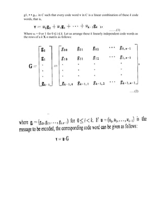
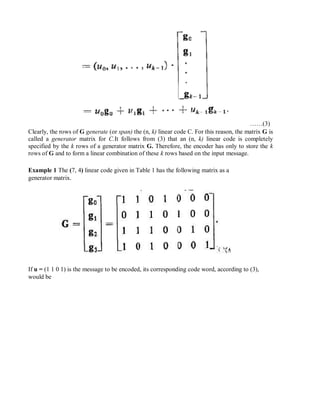
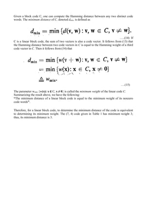
The document provides an overview of source coding in digital communication systems. It discusses the key elements of a communication system including the transmitter, receiver, and channel. It then describes how an analog information source is converted to a digital signal through sampling, quantization, and coding. Source coding aims to remove redundancy in the information so as to minimize the bandwidth required for transmission. Channel coding adds extra bits to help detect and correct errors. Line coding represents the digital bit stream as voltage or current variations suited for the transmission channel. Key techniques discussed include pulse code modulation (PCM), companding, and various line codes.