Download to read offline
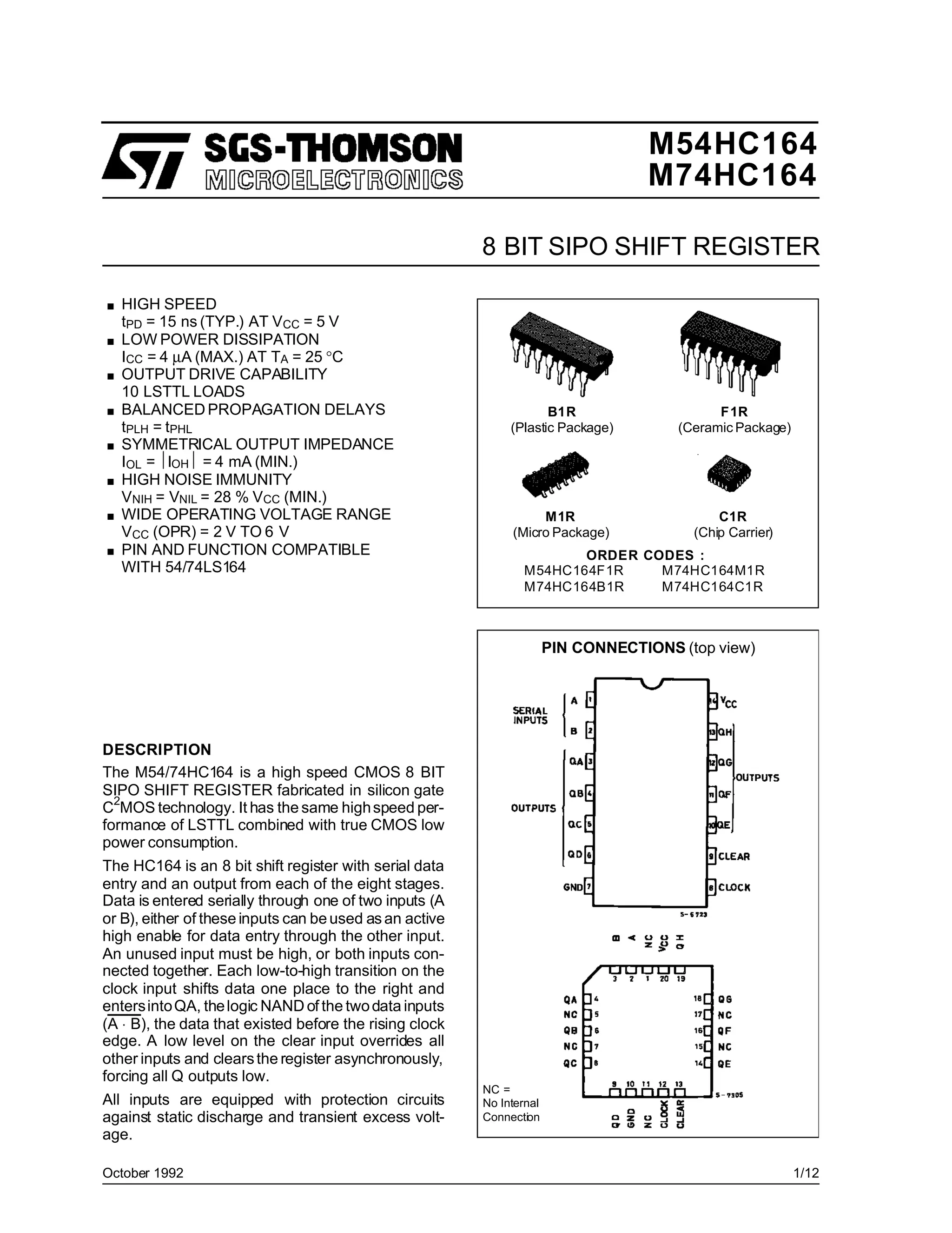
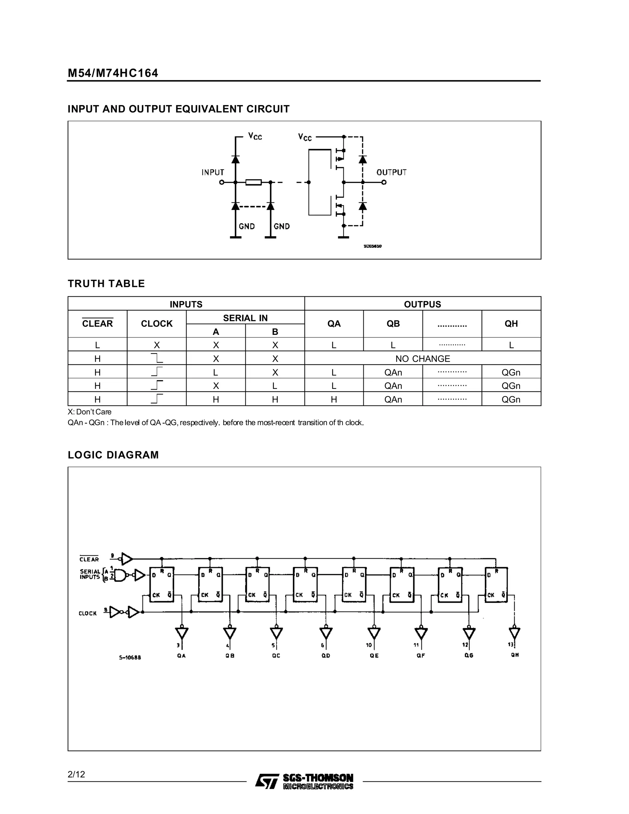


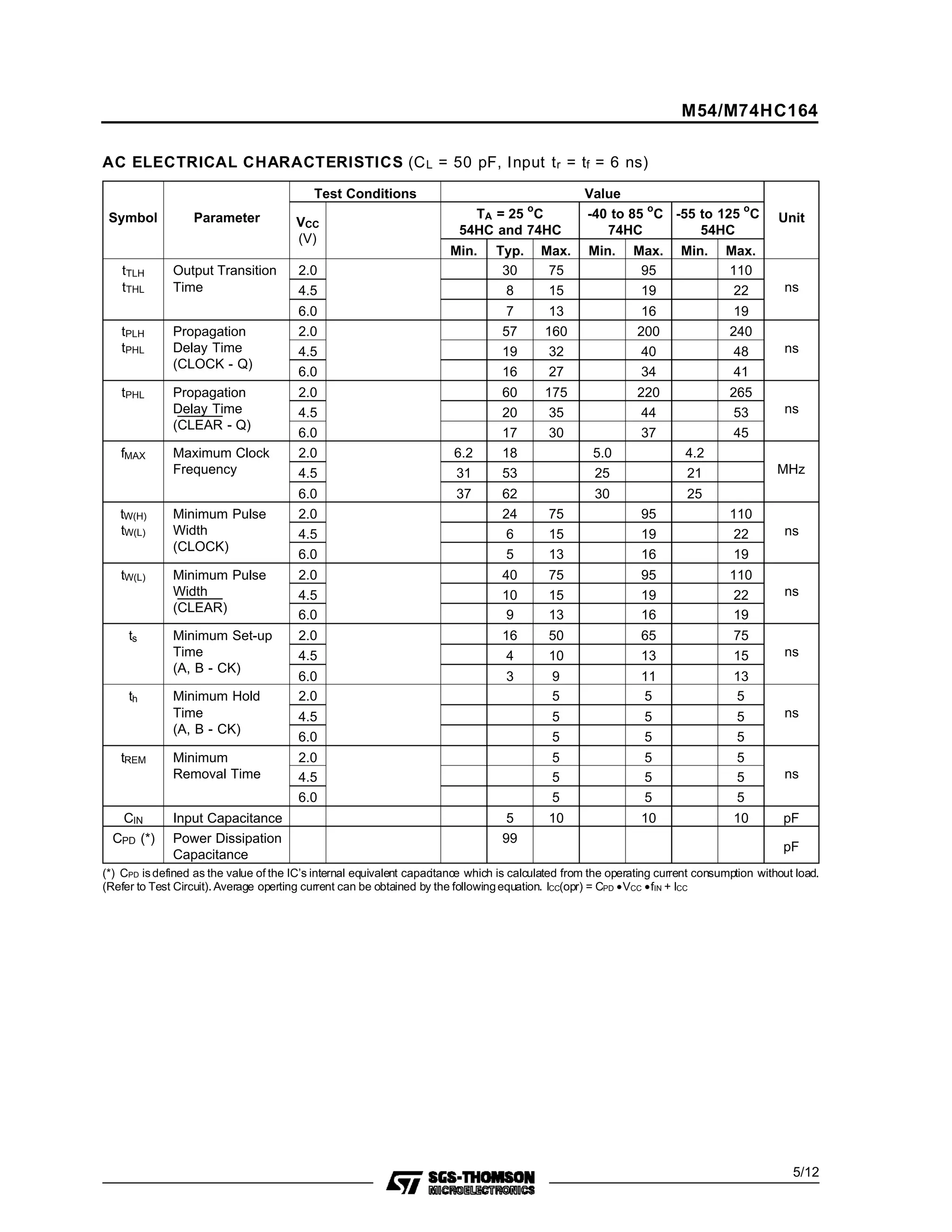


This document provides information on the M54HC164 and M74HC164 8-bit shift registers, including pin connections, logic diagram, truth table, timing diagrams, specifications, and mechanical drawings. Key details are that it is a high-speed CMOS shift register with serial data entry, low power consumption, and compatibility with 54/74LS164 registers. It has symmetrical propagation delays, high noise immunity, and a wide operating voltage range of 2-6V.


