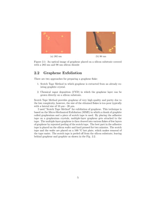
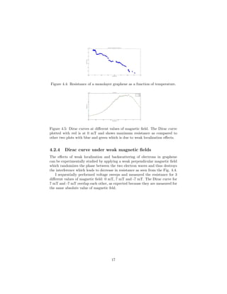
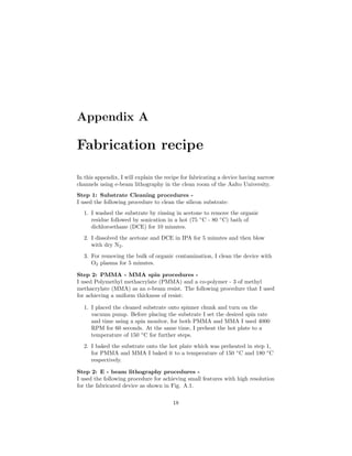
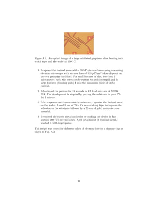
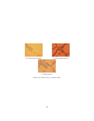
SlideShare a Scribd company logo
1 of 23
Download to read offline
Weak localization effects in
disordered graphene
Thesis Subtitle
Hemant Kumar
Department of Physics
Aalto University
Finland
Contents
1 Introduction 1
1.1 Band structure . . . . . . . . . . . . . . . . . . . . . . . . . . . . 1
1.2 Transport measurements in graphene . . . . . . . . . . . . . . . . 2
1.3 Weak localization . . . . . . . . . . . . . . . . . . . . . . . . . . 3
2 Device Fabrication 4
2.1 Cleaning of substrate . . . . . . . . . . . . . . . . . . . . . . . . . 4
2.2 Graphene Exfoliation . . . . . . . . . . . . . . . . . . . . . . . . . 5
2.3 Raman spectroscopy . . . . . . . . . . . . . . . . . . . . . . . . . 6
2.4 Lithography . . . . . . . . . . . . . . . . . . . . . . . . . . . . . . 8
2.4.1 Resist coating . . . . . . . . . . . . . . . . . . . . . . . . . 9
2.4.2 Electron Beam Exposure . . . . . . . . . . . . . . . . . . 9
2.5 Metalization . . . . . . . . . . . . . . . . . . . . . . . . . . . . . . 9
2.6 Lift-Off . . . . . . . . . . . . . . . . . . . . . . . . . . . . . . . . 10
2.7 Bonding . . . . . . . . . . . . . . . . . . . . . . . . . . . . . . . . 10
3 Measurement set-up 11
3.1 Measurement scheme . . . . . . . . . . . . . . . . . . . . . . . . . 11
3.2 Cryogenic apparatus . . . . . . . . . . . . . . . . . . . . . . . . . 12
3.3 Wiring . . . . . . . . . . . . . . . . . . . . . . . . . . . . . . . . . 12
4 Experimental part 14
4.1 Sample geometries . . . . . . . . . . . . . . . . . . . . . . . . . . 14
4.2 Electrical characterization of the device . . . . . . . . . . . . . . 14
4.2.1 Dirac curve . . . . . . . . . . . . . . . . . . . . . . . . . . 14
4.2.2 Carrier mobility . . . . . . . . . . . . . . . . . . . . . . . 16
4.2.3 Resistance variation with temperature . . . . . . . . . . . 16
4.2.4 Dirac curve under weak magnetic fields . . . . . . . . . . 17
A Fabrication recipe 19
1
Abstract
Graphene a perfect 2-D material made of carbon atoms two-dimensional elec-
tron gas lying on the surface. Due to the low spin-orbit coupling of carbon
atoms, graphene is an ideal candidate for the spin bus in spin transistors. The
fluctuation of residual charge densities due to its lattice defects and trapped
charge in gate oxide is main concern towards the realization of the spin bus in
graphene. The weak localization in graphene is a potential tool to characterize
such fluctuations. Here in this thesis, I probed the weak localization effects
in graphene on SiO2. For this, I fabricated the micrometer-sized graphene de-
vice and measured the conductance fluctuation in dilution refrigerator in the
presence of magnetic field.
Chapter 1
Introduction
In 2003, Andre Geim along with his colleague Kostya Novoselov took a block
of graphite and some Scotch tape. They repeatedly stuck and peeled back the
Scotch tape until they managed to get down to few atomic sheets of carbon
which produced a material that is an excellent conductor of heat and electricity
and has an extreme mechanical strength about 100 times stronger than the
strongest steel. In 2010, for his work in graphene, they won Nobel prize in
physics.
The purpose of this chapter is to give a brief review on the electronic prop-
erties of graphenes mainly from a theoretical point of view. Later on, I will also
present transport studies at a weak magnetic field on monolayer graphene, with
a particular emphasis on weak localization and backscattering of electrons.
1.1 Band structure
Graphene, a planar atomic sheet of carbon atoms arranged together in a densely
packed hexagonal honeycomb lattice with two atoms A and B per unit cell as
shown in Fig. 1.1. The stability of graphene, a 2-dimensional structure is due
to its tightly packed carbon atoms in which each carbon atom having an atomic
number of six and has an electronic configuration of 1s2
2s2
2p2
. The valence
electron of each carbon atoms in graphene is sp2
hybridized.
In graphene valence and conduction band form a conically shaped structure
which meets at the K and K points of the Brillouin zone and creates the zero
band gap (Fig. 1.1). The point, where the conduction and the valence band
touches each other is called the Dirac point. The low energy properties of
graphene in the vicinity of Dirac points (K, K ) satisfy the following equation:
E(k) = ±¯h × vf k2
x + k2
y
where a + sign corresponds to the conduction band and a - sign to the valence
band and vf is the Fermi velocity, vf = 1 × 10⁶
m/s.
1
Figure 1.1: Left to right: The honeycomb lattice of graphene in which a unit
cell is represented by a two carbon atoms denoted by A and B, the conduction
(upper) band and the valence (lower) band touches each other in six points of
a hexagon, the K and K points and linear dispersion at low energies.
1.2 Transport measurements in graphene
The basic graphene field-effect transistor (FET) consist of a graphene film with
two metal electrodes placed on a highly doped Si substrate as shown in Fig.
1.1 (a). The carrier density induced due to back gate voltage can be calculated
according to the following equation:
n =
o rVG
te
= αVg
where o is the permittivity of free space ( o = 8.854 × 10⁻¹²
F/m), r is the
relative permittivity of SiO2 ( r = 3.9) t is the thickness of SiO2 layer (in
our case t = 282 nm) and e is the electron charge (e = 1.602 × 10⁻¹⁹
C). After
substituting the values the proportionality coefficient α is found to be 7.64×10¹⁰
cm−2
V −1
.
The conductivity of a graphene strongly depends on the position of the
Fermi level. In an undoped graphene, the fermi level lies at the Dirac point
with a completely filled valence band and the empty conduction band. The
density of states and hence carrier concentration vanishes at the Dirac point and
becomes smaller than the charged impurity which results in the breakage of the
system into puddles of electrons and holes. The presence of charge impurities
in the form of puddles of electron and hole induce a density distribution in
the graphene sample which is responsible for the finite minimum conductivity.
The finite minimum conductivity can also be induced by several mechanisms
such as corrugations in the graphene sheet which shift the position of the Dirac
point, molecular doping, external gate voltage, thermal fluctuations and crystal
defects.
The dependence of the resistivity on gate voltage is shown in Fig. 1.2 (b).
In doped graphene fermi level is shifted from the Dirac point, depending on
the type of doping concentration. When the fermi level lies below or above the
Dirac point, the conduction is usually carried out by holes in the valence band
or electrons in the conduction band respectively. In doped graphene, the carrier
2
(a) Graphene FET (b) Dirac cone
Figure 1.2: Schematic diagram of a graphene field effect transistor with Si (P++
)
act as a back gate and conductance is measured between source and drain
through graphene and Dirac curve
Figure 1.3: An electron trajectory in a diffusive system which is not in the
straight line due to random scattering by charged impurities. The phase of the
electron waves is same as the two paths are identical and their interference will
be constructive in nature.
density at various gate voltages can be obtained from the relation:
n = α(Vg − VDirac)
where α = 7.64 × 10¹⁰
cm−2
V −1
from equation 1.1 and VDirac (Dirac voltage)
is the gate voltage for which the maximum resistivity is observed.
1.3 Weak localization
Weak localization is a well-known Quantum interference effects which arise at
low temperatures. Weak localization is usually due to the backscattering and
constructive interference between two paths of the electron along closed loops,
traveling in opposite directions as shown in Fig. 1.3. This constructive interfer-
ence increased the resistance of the sample, which is known as Weak localization
effects.
3
Chapter 2
Device Fabrication
The most basics fabrication of a graphene based device consists of follow-
ing steps: cleaning of the substrate, exfoliation of graphene, identification of
graphene using Raman spectroscopy, e-beam Lithography, metallization and
lift-off. In the final stage, in order to connect the device to measurement setup,
the chip is bonded to a chip carrier. In this chapter, I will explain aforemen-
tioned steps in details.
2.1 Cleaning of substrate
Graphene, a one-atom-thick sheet of carbon atoms need a substrate over which it
can be stabilized. Without an underlying substrate, a two-dimensional crystal
can not be thermally stable and it will wrinkle/crumbled. In general, a flat
substrate is preferred for a long mean free path in ballistic samples. The most
prevalent substrate is SiO2/Si. The thickness of the SiO2 has to be carefully
selected in order to have a good optical contrast. Oxide thickness of 90 nm and
282 nm is two such candidate for optical characterization of the graphene, 90
nm shows better contrast, see Fig. 2.1.
I choose 282 nm oxide Si P++
for our device fabrication where P-doped Si
acts as a back gate for our device. Thicker oxide allows us to use larger gate
voltage over the graphene without the electrical breakdown of the SiO2.
The substrate size at the low-temperature laboratory is of 5 mm×5 mm and
it has pre-patterned Ti/Au markers. Si chips usually contain organic residues
and Si/SiO2 debris. For organic residue, I washed the substrate in Acetone then
rinse in IPA which is then followed by oxygen plasma. For heavier debris like
SiO2 and Si, chips are sonicated in Acetone.
4
(a) 282 nm (b) 90 nm
Figure 2.1: An optical image of graphene placed on a silicon substrate covered
with a 282 nm and 90 nm silicon dioxide
2.2 Graphene Exfoliation
There are two approaches for preparing a graphene flake:
1. Scotch Tape Method in which graphene is extracted from an already ex-
isting graphite crystal.
2. Chemical vapor deposition (CVD) in which the graphene layer can be
grown directly on a silicon substrate.
Scotch Tape Method provides graphene of very high quality and purity due to
the low complexity, however, the size of the obtained flakes is too poor typically
with a lateral size of 10 µm - 20 µm.
I used ”Scotch Tape Method” for exfoliation of graphene. This technique is
based on the Micro-Mechanical Exfoliation (MME) in which a chunk of graphite
called graphenium and a piece of scotch tape is used. By placing the adhesive
tape on a graphenium crystals, multiple-layer graphene gets attached to the
tape. The multiple-layer graphene is then cleaved into various flakes of few layers
of graphene by repeated peeling of the scotch tape. The best part in the adhesive
tape is placed on the silicon wafer and hard pressed for two minutes. The scotch
tape and the wafer are placed on a 100 ◦
C hot plate, which makes removal of
the tape easier. The scotch tape is peeled off from the silicon substrate, leaving
behind graphene and graphite as shown in the Fig. 2.2.
5
Figure 2.2: An optical image of a large exfoliated graphene after heating both
scotch tape and the wafer at 100 ◦
C.
Figure 2.3: Raman spectra of mono-layer graphene fitted with a convolution of
Gaussian and Lorentzian function.
2.3 Raman spectroscopy
Raman spectroscopy is a spectroscopic technique based on inelastic scattering of
monochromatic laser light. In an Inelastic scattering the frequency of photons
in monochromatic light changes upon interaction with a sample. The thickness,
disorder, doping, strain and thermal conductivity of graphene can be learned
from the Raman spectrum. The position and shape of the two major Raman
bands G and 2D in graphene is one of the most important pieces of information
for physics of graphene and can be used for determining the number of layers.
Fig. 2.3 shows the G and 2D peak of the monolayer graphene.
The G band - The G band is a sharp band that appears around 1587 cm−1
in the Raman spectrum of graphene. The band is an in-plane vibrational mode
involving the sp2
hybridized carbon atoms that comprise the graphene sheet.
It is extremely sensitive to strain, doping, and temperature. The width and the
frequency of the G band can be used to monitor the doping level in graphene.
The position of the G band shifts to lower energy as the layer thickness
increases representing the softening of the bonds between carbon atoms.
6
0 0.5 1 1.5 2 2.5 3 3.5 4
1572
1574
1576
1578
1580
1582
1584
1586
1588
1590
layers
Gpeakposition(1/cm)
G peak position vs number of layers
0 0.5 1 1.5 2 2.5 3 3.5 4
2660
2665
2670
2675
2680
2685
2690
2695
layers
2Dpeak(1/cm)
2D peak position vs number of layers
0 0.5 1 1.5 2 2.5 3 3.5 4
5
10
15
20
25
layers
GpeakFWHM(1/cm)
G Peak FWHM vs number of layers
0 0.5 1 1.5 2 2.5 3 3.5 4
30
40
50
60
70
layers
2DpeakFWHM(1/cm)
2D Peak FWHM vs number of layers
Figure 2.4: Comparison of Raman G and 2D peaks of the monolayer, bilayer,
trilayer graphene. The substrate (Si with 282 nm SiO2) and laser wavelength
(633 nm) are the same for all samples.
The D band - The D band is known as the disorder band or the defect band and
is due to lattice motion away from the center of the Brillouin zone. It appears
between 1270 and 1450 cm−1
, indicates defects or edges in the graphene sample.
The D band is typically weak in high-quality graphene. The intensity of the D
band is directly proportional to the level of defects in the sample.
The 2D band - The 2D band is referred to as an overtone of the D band and
it is the result of a two-phonon lattice vibrational process. The 2D band is a
strong band in graphene and it appears at approximately 2700 cm−1
. The
position and shape of the 2D band depend on the excitation frequency of the
laser and can be used for the determining the number of layers in graphene.
The peak positions and full-width half maximum (FWHMs) of G and 2D peaks
have been plotted as a function of the number of layers as shown in Fig. 2.4.
The peak intensity ratio of the 2D and G band can also be used to identify
the monolayer graphene. The ratio I2D/IG of these bands for a high-quality
single-layer graphene will be seen to be equal to 2 as shown in Fig. 2.5.
The Raman spectrum curve is fitted with a convolution of a Lorentzian and
a Gaussian function to get a more accurate value for the full width at half
maximum (FWHM). The G peak doesnt give sufficient information to distin-
guish between different thicknesses, on the other hand, the 2D peak position
or FWHM, provides a definite method for identifying monolayer graphene. In
Fig. 2.4, the positions and FWHMs of G and 2D peaks have been plotted as a
function of the number of layers.
7
1.5 1.6 1.7 1.8 1.9 2 2.1 2.2 2.3 2.4 2.5
0.5
0.6
0.7
0.8
0.9
1
1.1
1.2
1.3
1.4
1.5
I2D
/IG
Monolayer
I2D
/IG
for Monolayer graphene
Figure 2.5: Intensity ratio of the 2D and G band for identification of a monolayer
graphene.
Figure 2.6: A schematic flowchart to fabricate a field effect transistor (FET)
2.4 Lithography
In the low-temperature laboratory, I used electron beam lithography to fabricate
the electrical leads to the graphene. The substrate is spin coated and using a
focused beam of electrons the pattern is exposed to form a negative mask. The
exposed resist is subsequently developed using a specific developer to create
a negative mask. A metal layer is then evaporated using e-beam evaporator
which metallized the fabricated leads. The remaining resist and excess metal
are removed using a solvent in the ”lift-off” process. A schematic diagram as
shown in Fig. 2.6, describes the process of making an electrical lead to the
graphene.
8
2.4.1 Resist coating
A thin layer of the resist of uniform thickness, to cover the substrate for lithog-
raphy process is achieved by using resist coating. The substrate is usually baked
at 150◦
C for 10 minutes before spinning to remove water which may cause poor
resist adhesion. I used PMMA and a copolymer - 3 of methyl methacrylate and
methacrylic acid (MMA-MAA) e-beam resist with a minimum baking temper-
ature of 180◦
C and 150◦
respectively for 5 minutes. I used a double-layer resist
because it provides a greater gain in resolution as compared to a thick single
layer resist.
The resist is then pipetted onto the substrate while the device is placed on
a spin coater which has a vacuum that holds the device being spun. During
the rotation the resist thickness decreases until a balance between adhesion and
centrifugal force is reached. The thickness of a particular resist is determined
by the spinning speed and resist concentration. The resulting resist coating has
some bulging at the edges and a uniform thickness at the center.
2.4.2 Electron Beam Exposure
In electron beam lithography (EBL), the resist is exposed to the desired elec-
trode pattern to fabricate the metallization mask. I made the pattern using
computer-aided design (CAD) software. The design CAD file is then converted
into a format that is readable by lithography system. The lithography system
sends commands to a scan generator which rasters focussed electron beam over
the resist. The movement of the e-beam is controlled by applying discrete volt-
age steps to deflection coils of electron column. A beam blanker is used when
the beam shifts to different parts of the pattern. A high-resolution pattern is
obtained by optimizing the total pixel dose, so that pattern did not get overex-
posed or underexposed. The optimum pixel dose is determined experimentally
to a dummy chip and the process is called dose test.
After exposure to the e-beam, the device is developed using a developer, for
PMMA and copolymer, I used methyl isobutyl ketone (MIBK). I diluted the
MIBK with isopropanol to achieve a high resolution. The development time for
2-layer resist in 1:3 MIBK : IPA is 7-10 second and depends on the thickness
of resist. The development process is usually stopped by rinsing the device in
pure IPA.
2.5 Metalization
Physical vapor deposition techniques are used to metallized the resist mask
created by e-beam lithography. The masked substrate is placed in a vacuum
chamber and the metal is evaporated from a crucible. During deposition the
pressure in the crucible range from 10−5
mbar to less than 10−9
mbar so that
the particles from the source do not collide with the gas molecules.
The material which sits in a water-cooled copper hearth is heated using
a focused electron beam. The e-beam is generated by heating a filament to
9
produce electrons which are then accelerated using high voltages (5 kV to 20
kV). The electron beam is focussed onto the copper hearth using magnetic and
electric fields.
The evaporated metal condensed on the masked substrate where the thick-
nesses of metal range from a few nanometers to thousands of nanometers with
a deposition rate of 0.1 nm/s to 10 nm/s. A quartz oscillator which sits in the
vacuum monitored the thickness of the evaporated material. The properties
of the evaporated metal depend on vacuum level, deposition rate, and process
residues. For low contact resistance to graphene, low vacuum pressure, and low
deposition rates are required.
An addition layer of different metal generally consists of 5 nm of Cr or Ti
is used to improve adhesion to the substrate followed by the main electrode
material. I used Gold of thickness 50nm for all superconducting contacts to
graphene.
2.6 Lift-Off
The process of removing the resist and excess metal after metallizing the con-
tacts is commonly referred to as lift-off. In this step, the resist and excess metal
are dissolved in an organic solvent. For PMMA and copolymer, I used acetone.
The lift-off can be accelerated by heating the acetone at 60 ◦
C and using a
syringe to spray acetone on the resist. After detachment of residual metal, the
device is washed with IPA and subsequently dried using pressurized nitrogen.
2.7 Bonding
It is a micro-welding technique for electrical interconnection of the device to
the PCB part of the sample holder using electrically insulating low-temperature
varnish. The electrical contacts between the bonding pads on the substrate and
aluminum wire are achieved using ultrasonic bonding. The size of the on-chip
bonding pads influences the performance of the device. I used bonding pads
of size 200 µm × 200 µm to avoid parasitic capacitances which can tune the
electronic property of the device.
For details fabrication recipe, please look into supplemental information:
Appendix A.
10
Chapter 3
Measurement set-up
In electronics transport measurements, the fabricated device needs to be pro-
tected from the outside world through cooling and shielding, while keeping them
connected to the macroscopic measurement setup. In this chapter, measurement
scheme, cryogenic setups used for cooling and the wiring will be addressed.
3.1 Measurement scheme
The measurement scheme for electrical characterisation of the device is pre-
sented in Fig. 3.1. I performed all the measurements using current biased
lock-in scheme. The phase lock-in AC transport measurements have a better
signal to noise ratio in comparison to dc measurement.
A reference sinusoidal signal of fixed amplitude and frequency from lock-in
(Stanford Research System SR830) is fed to sample through a high resistance
for current bias measurement. The signal from the sample is filtered to remove
the high-frequency components and amplified using current to voltage pream-
plifier (SR 570). The output of the preamplifier is measured with respect to the
reference signal in lock-in.
The back gate of the sample is connected to a Keithley voltage source. An
external current carrying coil is used to produce a low magnetic field in the
range between -7 to 7 milli tesla (mT).
The controlled voltage from lock-in is sent to a current source which is then
fed into the coil. The current in the coil generates an induced magnetic field
which is given by the following expression:
B =
µoNiR2
2(R2 + z2)1/2
where R is the radius of the current carrying loop, i is the current, N is the
number of turns, z is the distance to axis of the loop from the centre and µo
is the permmeability of free space (µo = 12.57 × 10⁻⁷
T-m/A). A computer
11
Figure 3.1: Scheme of the measurement setup.
records the amplitude and phase of the detected signal, the back gate voltage
and the current delivered to the electromagnet.
3.2 Cryogenic apparatus
The quantum behavior in fabricated graphene device required a minimum tem-
perature of 20 mK or below. A dilution refrigerator is a most convenient way
to provide continuous cooling to temperatures as low as 2 mK. The cooling
power is generated by the mixing of the helium-3 (He-3) ’lighter concentrated
phase’ and helium-4 (He-4) ’heavier dilute phase’ in the mixing chamber. In a
continuous cooling system helium-3 (He-3) must be extracted from the heavier
dilute phase and returned into the lighter concentrated phase. This is achieved
by distilling of helium-3 (He-3) in a still which is internally connected by the
pumping lines to the heavier diluted phase in the mixing chamber. A resistive
heater in the still is used to maximize the evaporation rate of helium-3(He-3).
These pumping lines are attached to the heat exchanger which carry away
heat from the mixing chamber where the experiment is thermally isolated. The
minimum achievable temperature was reached in a piece of rhodium metal using
a slightly different technique (nuclear de-magnetism), which was cooled to 100
pK. This record is achieved in the low-temperature laboratory, Helsinki where
I did my internship.
3.3 Wiring
Electronic transport measurements at cryogenic temperatures require wires that
connect room-temperature electronics to the sample. However, transmission of
signals through these measurement lines is affected by electromagnetic radia-
tion from the outside. A strong filtering is usually required to suppress high-
frequency noise. These lines are filtered using multiple filtering techniques to
12
create a high attenuation over a wide frequency range.
Manganin twisted pairs - Manganin twisted pairs, an alloy made up of 83%
copper, 13% manganese, and 4% nickel. It is used to connect 4 K cold plate to
the outside world thus minimizing heat transfer between two points and to
minimize electromagnetic noise pick-up. The resistivity of twisted pairs is
around 60 /m along with a distributed capacitance of 330pF/m which provides
a large attenuation at high frequencies with a cut-off frequency around 1 GHz.
Thermocoax - All measurement lines from 4.2K to cold plate use
thermocoax cables, which additionally filter the high frequencies components.
At mixing chamber plate, the additional filtering is added by integrating
copper powder filter and RC filter inside the shielded box to eliminate
electromagnetic noise. The overall, filter of the dc wiring is in the range of 10
kHz. Copper powder filter also provides thermal equilibrium of the electric
leads from high-temperature parts of a cryostat. These signals are further
filtered at different stages using RLC filter which prevents the sample from the
high voltage spikes. A lock-in amplifier of high sensitivity is used to detects
the signals from the sample.
Shielded sample stage - In transport measurements, the device and
measurement electronics were placed inside of the electromagnetically shielded
box. This box is usually made of copper or brass. The cover is sealed making
the box vacuum and radiation tight.
13
Chapter 4
Experimental part
4.1 Sample geometries
In transport measurements, several sample geometries can be used to investigate
the intrinsic behavior of graphene. In simplest two terminal measurements, the
two leads are used for both as current leads and for voltage measurement. The
current from the current source results in a voltage drop in the graphene and
contacts, giving additional resistance. A voltmeter measures the voltage drop
between the sample electrodes, as shown in Fig. 4.1 (a). The measured voltage:
V ≈ I(Rsample + 2rcontact)
Finally, with the four-terminal configuration, one can exclude the wire impedance
from the measurement. The current is fed through the electrode connected to
the graphene sample and the voltage drop is measured from the central section
of the sample as shown in Fig. 4.1 (b). The measured voltage:
V = (I − i)Rsample − i(2rcontact + 2rlead)
V ≈ IRsample
4.2 Electrical characterization of the device
4.2.1 Dirac curve
In the experiments, I investigated two graphene field effect transistor of different
channel length, for which I measured the resistivity versus charge density using
four-terminal configuration. Before cooling down the sample to mK tempera-
ture, I scanned the graphene resistance as a function of the charge density (n)
at room temperature as shown in the Fig. 4.2.
The position of the Dirac point, where maximum resistivity is observed de-
pends on initial doping concentration. Usually, because of the initial doping,
14
(a) (b)
Figure 4.1: (a) Two-terminal configurations and (b) four-terminal configuration
used for transport measurements.
−8 −6 −4 −2 0 2 4 6 8
x 10
11
800
900
1000
1100
1200
1300
1400
1500
1600
1700
1800
Charge density (n)
Resistivity(Ω)
Resistivity vs Charge density at room temperature (292.3495K)
(a) Graphene resistivity as a function of
charge density at room temperature.
0 0.5 1 1.5 2 2.5 3
x 10
12
1000
2000
3000
4000
5000
6000
7000
charge density (n)
Resistivity(Ω)
Resistivity vs Charge density at 630 mK while cooling down
(b) D1
−4 −3 −2 −1 0 1 2
x 10
12
0.2
0.4
0.6
0.8
1
1.2
1.4
1.6
1.8
x 10
5
Charge density (n)
Resistance(Ω)
Resistance vs Charge density at 1K
(c) D2
Figure 4.2: Dirac curve for device (a) D1 having scaling factor w/l = 0.187 (b)
D2 having scaling factor w/l = 1.15.
the position of the Dirac point shifts from the ideal curve. The initial doping in
graphene can be calculated by measuring the FWHM of a fitted 2-dimensional
gaussian curve to resistivity versus charge density plot as shown in Fig. 4.2 (b,
c). The initial doping is calculated to be for device D1: n = 1.6 × 10¹²
cm−2
and for device D2: 3.2857 × 10¹²
cm−2
. The scaling factor from resistance to
sheet resistance for device (D1) is w/l = 0.187, for device (D2) is w/l = 1.15.
The obtained resistivity versus gate voltage curves was very broad this can
be explained by thermodynamics stability of the two-dimensional (2D) mate-
rial. The stability of graphene is due to the presence of large three-dimensional
bulk structure beneath which cause microscopic corrugations in graphene. As
15
−2.5 −2 −1.5 −1 −0.5 0 0.5 1
x 10
12
0
1
2
3
4
5
6
7
8
x 10
−4
Charge density
Electricalconductivity
Conductivity vs Charge density
Figure 4.3: Conductivity of a graphene measured as a function of charge density.
The ratio of the slope of the linear fits indicates that in this sample mobility of
electrons is not equal to the mobility of holes.
a result, the position of the Dirac point is not constant for the whole graphene
sheet which causes the broadening of the density of states.
4.2.2 Carrier mobility
The mobility of electrons/holes is affected by the strength of intrinsic or extrin-
sic scattering mechanisms. Intrinsic scattering is caused due to scattering of
phonons while extrinsic includes scattering due to defects, impurities or adsor-
bates. The extrinsic scattering caused by impurities implies the purity of the
sample and can be increased with technological improvement.
In undoped graphene, the strength of the intrinsic scattering is same for both
electrons or holes and does not depend on charge hence the electron mobility µe
is equal to the hole mobility µh. The mobility of the electron and hole can be
verified experimentally by measuring the electrical conductivity as a function of
gate voltage as shown in Fig. 4.3.
σ(Vg) = ni(Vg)eµi
where ni(Vg) is the concentration of charge carriers electrons or holes calculated
in chapter 1. The plot between electrical conductivity and gate voltage shows
a linear dependence and the ratio of the slope of lines gives the mobility, here
| µe/µh | ≈ 0.8. Thus, the ratio between mobilities of electrons and holes is not
universal and depends on the quality and quantity of impurity in graphene.
4.2.3 Resistance variation with temperature
I measured the resistance of monolayer graphene using the field effect transistor
configuration as a function of temperature at a constant gate voltage (Vg = -
12.6 V) near the charge neutrality point. At higher temperature (above around
150 K) resistance increases with temperature due to scattering from high energy
phonons. But below around 400 mK resistance often decreases as increase in
temperature as shown in Fig. 4.4. This behavior suggests that resistivity at
charge neutrality point is usually governed by charged impurities puddles of
electrons and holes.
16
Figure 4.4: Resistance of a monolayer graphene as a function of temperature.
−60 −50 −40 −30 −20 −10 0 10
0
5
10
15
x 10
4
Gate Voltage (V)
Resistance(Ω)
R vs Vg at 1K
7 mT
0 mT
−7 mT
Figure 4.5: Dirac curves at different values of magnetic field. The Dirac curve
plotted with red is at 0 mT and shows maximum resistance as compared to
other two plots with blue and green which is due to weak localization effects.
4.2.4 Dirac curve under weak magnetic fields
The effects of weak localization and backscattering of electrons in graphene
can be experimentally studied by applying a weak perpendicular magnetic field
which randomizes the phase between the two electron waves and thus destroys
the interference which leads to decrease in resistance as seen from the Fig. 4.4.
I sequentially performed voltage sweeps and measured the resistance for 3
different values of magnetic field: 0 mT, 7 mT and -7 mT. The Dirac curve for
7 mT and -7 mT overlap each other, as expected because they are measured for
the same absolute value of magnetic feld.
17
Appendix A
Fabrication recipe
In this appendix, I will explain the recipe for fabricating a device having narrow
channels using e-beam lithography in the clean room of the Aalto University.
Step 1: Substrate Cleaning procedures -
I used the following procedure to clean the silicon substrate:
1. I washed the substrate by rinsing in acetone to remove the organic
residue followed by sonication in a hot (75 ◦
C - 80 ◦
C) bath of
dichloroethane (DCE) for 10 minutes.
2. I dissolved the acetone and DCE in IPA for 5 minutes and then blow
with dry N2.
3. For removing the bulk of organic contamination, I clean the device with
O2 plasma for 5 minutes.
Step 2: PMMA - MMA spin procedures -
I used Polymethyl methacrylate (PMMA) and a co-polymer - 3 of methyl
methacrylate (MMA) as an e-beam resist. The following procedure that I used
for achieving a uniform thickness of resist:
1. I placed the cleaned substrate onto spinner chunk and turn on the
vacuum pump. Before placing the substrate I set the desired spin rate
and time using a spin monitor, for both PMMA and MMA I used 4000
RPM for 60 seconds. At the same time, I preheat the hot plate to a
temperature of 150 ◦
C for further steps.
2. I baked the substrate onto the hot plate which was preheated in step 1,
for PMMA and MMA I baked it to a temperature of 150 ◦
C and 180 ◦
C
respectively.
Step 2: E - beam lithography procedures -
I used the following procedure for achieving small features with high resolution
for the fabricated device as shown in Fig. A.1.
18
Figure A.1: An optical image of a large exfoliated graphene after heating both
scotch tape and the wafer at 100 ◦
C.
1. I exposed the desired areas with a 20 kV electron beam using a scanning
electron microscope with an area does of 200 µC/cm2
(does depends on
pattern geometry and size). For small features of size, less than 1
micrometer I used the lowest probe current to avoid overspill and for
large features (bonding pads) I used the maximum value of probe
current.
2. I developed the pattern for 15 seconds in 1:3 fresh mixture of MIBK :
IPA. The development is stopped by putting the substrate in pure IPA
for 1 minute.
3. After exposure to e-beam onto the substrate, I sputter the desired metal
on the wafer. I used 5 nm of Ti or Cr as a sticking layer to improve the
adhesion to the substrate followed by a 50 nm of gold, main electrode
material.
4. I removed the excess metal and resist by soaking the device in hot
acetone (60 ◦
C) for two hours. After detachment of residual metal, I
washed it with isopropanol.
This recipe was tested for different values of electron dose on a dummy chip as
shown in Fig. A.2.
19
(a) Underexposed pattern (b) Overexposed pattern
(c) Ideal pattern
Figure A.2: Dose test on a dummy chip.
20

More Related Content

What's hot

Graphene and hexagonal boron nitride filled epoxy nanocomposites
Graphene and hexagonal boron nitride filled epoxy nanocompositesGraphene and hexagonal boron nitride filled epoxy nanocomposites
Graphene and hexagonal boron nitride filled epoxy nanocompositesArun Yadav
 
15.30 o5 a kaiser
15.30 o5 a kaiser15.30 o5 a kaiser
15.30 o5 a kaiserNZIP
 
Multipactor prevention mulcopim 11 technology description
Multipactor prevention mulcopim 11 technology descriptionMultipactor prevention mulcopim 11 technology description
Multipactor prevention mulcopim 11 technology descriptionIgor_Kossyi
 
Graphene MOSFET
Graphene MOSFETGraphene MOSFET
Graphene MOSFETPawan Bang
 
Reflectance and photoluminescence characterization of BexZn1
Reflectance and photoluminescence characterization of BexZn1Reflectance and photoluminescence characterization of BexZn1
Reflectance and photoluminescence characterization of BexZn1Oleg Maksimov
 
Study of the formation of Cold Fronts and Radio Mini-halos induced by the Int...
Study of the formation of Cold Fronts and Radio Mini-halos induced by the Int...Study of the formation of Cold Fronts and Radio Mini-halos induced by the Int...
Study of the formation of Cold Fronts and Radio Mini-halos induced by the Int...khanmuhammad
 
Shulze - Surface and Thin Film Characterization of Superconducting Multilayer...
Shulze - Surface and Thin Film Characterization of Superconducting Multilayer...Shulze - Surface and Thin Film Characterization of Superconducting Multilayer...
Shulze - Surface and Thin Film Characterization of Superconducting Multilayer...thinfilmsworkshop
 
Pd-Substituted (La,Sr)CrO3 for Solid Oxide Fuel Cell Anodes
Pd-Substituted (La,Sr)CrO3 for Solid Oxide Fuel Cell AnodesPd-Substituted (La,Sr)CrO3 for Solid Oxide Fuel Cell Anodes
Pd-Substituted (La,Sr)CrO3 for Solid Oxide Fuel Cell AnodesEmmaReneeDutton
 
Dielectric, Electric and Thermal Behavior of La3+ doped Co-Zn Nanoferrite
Dielectric, Electric and Thermal Behavior of La3+ doped Co-Zn NanoferriteDielectric, Electric and Thermal Behavior of La3+ doped Co-Zn Nanoferrite
Dielectric, Electric and Thermal Behavior of La3+ doped Co-Zn NanoferriteIOSRJAP
 

What's hot (19)

Graphene and hexagonal boron nitride filled epoxy nanocomposites
Graphene and hexagonal boron nitride filled epoxy nanocompositesGraphene and hexagonal boron nitride filled epoxy nanocomposites
Graphene and hexagonal boron nitride filled epoxy nanocomposites
 
SOFC perovskite- DFT work
SOFC perovskite- DFT workSOFC perovskite- DFT work
SOFC perovskite- DFT work
 
93 pooja
93 pooja93 pooja
93 pooja
 
N035489094
N035489094N035489094
N035489094
 
15.30 o5 a kaiser
15.30 o5 a kaiser15.30 o5 a kaiser
15.30 o5 a kaiser
 
Af25175180
Af25175180Af25175180
Af25175180
 
Lecture 01
Lecture 01Lecture 01
Lecture 01
 
6-oc ceramic kilowatts
6-oc ceramic kilowatts6-oc ceramic kilowatts
6-oc ceramic kilowatts
 
Multipactor prevention mulcopim 11 technology description
Multipactor prevention mulcopim 11 technology descriptionMultipactor prevention mulcopim 11 technology description
Multipactor prevention mulcopim 11 technology description
 
Sofc
SofcSofc
Sofc
 
Lv3520212024
Lv3520212024Lv3520212024
Lv3520212024
 
MASc Research work
MASc Research workMASc Research work
MASc Research work
 
Graphene MOSFET
Graphene MOSFETGraphene MOSFET
Graphene MOSFET
 
Reflectance and photoluminescence characterization of BexZn1
Reflectance and photoluminescence characterization of BexZn1Reflectance and photoluminescence characterization of BexZn1
Reflectance and photoluminescence characterization of BexZn1
 
Study of the formation of Cold Fronts and Radio Mini-halos induced by the Int...
Study of the formation of Cold Fronts and Radio Mini-halos induced by the Int...Study of the formation of Cold Fronts and Radio Mini-halos induced by the Int...
Study of the formation of Cold Fronts and Radio Mini-halos induced by the Int...
 
Shulze - Surface and Thin Film Characterization of Superconducting Multilayer...
Shulze - Surface and Thin Film Characterization of Superconducting Multilayer...Shulze - Surface and Thin Film Characterization of Superconducting Multilayer...
Shulze - Surface and Thin Film Characterization of Superconducting Multilayer...
 
Pd-Substituted (La,Sr)CrO3 for Solid Oxide Fuel Cell Anodes
Pd-Substituted (La,Sr)CrO3 for Solid Oxide Fuel Cell AnodesPd-Substituted (La,Sr)CrO3 for Solid Oxide Fuel Cell Anodes
Pd-Substituted (La,Sr)CrO3 for Solid Oxide Fuel Cell Anodes
 
Ij3614591468
Ij3614591468Ij3614591468
Ij3614591468
 
Dielectric, Electric and Thermal Behavior of La3+ doped Co-Zn Nanoferrite
Dielectric, Electric and Thermal Behavior of La3+ doped Co-Zn NanoferriteDielectric, Electric and Thermal Behavior of La3+ doped Co-Zn Nanoferrite
Dielectric, Electric and Thermal Behavior of La3+ doped Co-Zn Nanoferrite
 

Viewers also liked

Kobetasonik09 Horarios
Kobetasonik09 HorariosKobetasonik09 Horarios
Kobetasonik09 Horariosguest304bf0ab
 
MediaEval 2015 - EURECOM @ SAVA2015: Visual Features for Multimedia Search
MediaEval 2015 - EURECOM @ SAVA2015: Visual Features for Multimedia SearchMediaEval 2015 - EURECOM @ SAVA2015: Visual Features for Multimedia Search
MediaEval 2015 - EURECOM @ SAVA2015: Visual Features for Multimedia Searchmultimediaeval
 

Viewers also liked (8)

Word
WordWord
Word
 
22
2222
22
 
8 minutos
8 minutos8 minutos
8 minutos
 
DownloadReport (5)
DownloadReport (5)DownloadReport (5)
DownloadReport (5)
 
Kobetasonik09 Horarios
Kobetasonik09 HorariosKobetasonik09 Horarios
Kobetasonik09 Horarios
 
Solidworks sap2000-in ventor
Solidworks sap2000-in ventorSolidworks sap2000-in ventor
Solidworks sap2000-in ventor
 
MediaEval 2015 - EURECOM @ SAVA2015: Visual Features for Multimedia Search
MediaEval 2015 - EURECOM @ SAVA2015: Visual Features for Multimedia SearchMediaEval 2015 - EURECOM @ SAVA2015: Visual Features for Multimedia Search
MediaEval 2015 - EURECOM @ SAVA2015: Visual Features for Multimedia Search
 
Nuevas Tecnologías
Nuevas TecnologíasNuevas Tecnologías
Nuevas Tecnologías
 

Similar to AALTO_THESIS

TunnelSpectroscopy v2
TunnelSpectroscopy v2TunnelSpectroscopy v2
TunnelSpectroscopy v2Arash Zeinali
 
Graphene -Applications in Electronics
Graphene -Applications in ElectronicsGraphene -Applications in Electronics
Graphene -Applications in ElectronicsZaahir Salam
 
Sputtering of Ga-doped ZnO nanocoatings on silicon for piezoelectric transducers
Sputtering of Ga-doped ZnO nanocoatings on silicon for piezoelectric transducersSputtering of Ga-doped ZnO nanocoatings on silicon for piezoelectric transducers
Sputtering of Ga-doped ZnO nanocoatings on silicon for piezoelectric transducersMariya Aleksandrova
 
Giant magnetoresistance ppt
Giant magnetoresistance pptGiant magnetoresistance ppt
Giant magnetoresistance ppttedoado
 
daniel_manuscript
daniel_manuscriptdaniel_manuscript
daniel_manuscriptDaniel Oler
 
Application of Graphene in electronics
Application of Graphene in electronicsApplication of Graphene in electronics
Application of Graphene in electronicsChinmay Chepurwar
 
Master Thesis: Thermal annealing of ZnO and sapphire (Al2O3) substrates
Master Thesis: Thermal annealing of ZnO and sapphire (Al2O3) substrates Master Thesis: Thermal annealing of ZnO and sapphire (Al2O3) substrates
Master Thesis: Thermal annealing of ZnO and sapphire (Al2O3) substrates Banaz M Hawrami
 
Mse phd lecture
Mse phd lectureMse phd lecture
Mse phd lectureToru Hara
 
Graphene Field Effect Transistor
Graphene Field Effect TransistorGraphene Field Effect Transistor
Graphene Field Effect TransistorAhmed AlAskalany
 
Synthesis and characterisation of k doped zno 1
Synthesis and characterisation of k doped zno 1Synthesis and characterisation of k doped zno 1
Synthesis and characterisation of k doped zno 1Jeslin Mattam
 
Research Inventy : International Journal of Engineering and Science is publis...
Research Inventy : International Journal of Engineering and Science is publis...Research Inventy : International Journal of Engineering and Science is publis...
Research Inventy : International Journal of Engineering and Science is publis...researchinventy
 

Similar to AALTO_THESIS (20)

TunnelSpectroscopy v2
TunnelSpectroscopy v2TunnelSpectroscopy v2
TunnelSpectroscopy v2
 
Graphene -Applications in Electronics
Graphene -Applications in ElectronicsGraphene -Applications in Electronics
Graphene -Applications in Electronics
 
Sputtering of Ga-doped ZnO nanocoatings on silicon for piezoelectric transducers
Sputtering of Ga-doped ZnO nanocoatings on silicon for piezoelectric transducersSputtering of Ga-doped ZnO nanocoatings on silicon for piezoelectric transducers
Sputtering of Ga-doped ZnO nanocoatings on silicon for piezoelectric transducers
 
Giant magnetoresistance ppt
Giant magnetoresistance pptGiant magnetoresistance ppt
Giant magnetoresistance ppt
 
proposal
proposalproposal
proposal
 
daniel_manuscript
daniel_manuscriptdaniel_manuscript
daniel_manuscript
 
Graphene2008
Graphene2008Graphene2008
Graphene2008
 
20320140501011
2032014050101120320140501011
20320140501011
 
Application of Graphene in electronics
Application of Graphene in electronicsApplication of Graphene in electronics
Application of Graphene in electronics
 
A0360105
A0360105A0360105
A0360105
 
Et36891896
Et36891896Et36891896
Et36891896
 
Master Thesis: Thermal annealing of ZnO and sapphire (Al2O3) substrates
Master Thesis: Thermal annealing of ZnO and sapphire (Al2O3) substrates Master Thesis: Thermal annealing of ZnO and sapphire (Al2O3) substrates
Master Thesis: Thermal annealing of ZnO and sapphire (Al2O3) substrates
 
Mse phd lecture
Mse phd lectureMse phd lecture
Mse phd lecture
 
Graphene Field Effect Transistor
Graphene Field Effect TransistorGraphene Field Effect Transistor
Graphene Field Effect Transistor
 
presentation
presentationpresentation
presentation
 
Synthesis and characterisation of k doped zno 1
Synthesis and characterisation of k doped zno 1Synthesis and characterisation of k doped zno 1
Synthesis and characterisation of k doped zno 1
 
Research Inventy : International Journal of Engineering and Science is publis...
Research Inventy : International Journal of Engineering and Science is publis...Research Inventy : International Journal of Engineering and Science is publis...
Research Inventy : International Journal of Engineering and Science is publis...
 
Bj26404407
Bj26404407Bj26404407
Bj26404407
 
ELECTRODEPOSITION OF SILVER NANOPARTICLES ON CARBON SPHERE SURFACES BY PULSE ...
ELECTRODEPOSITION OF SILVER NANOPARTICLES ON CARBON SPHERE SURFACES BY PULSE ...ELECTRODEPOSITION OF SILVER NANOPARTICLES ON CARBON SPHERE SURFACES BY PULSE ...
ELECTRODEPOSITION OF SILVER NANOPARTICLES ON CARBON SPHERE SURFACES BY PULSE ...
 
G24041050
G24041050G24041050
G24041050
 

AALTO_THESIS

  • 1. Weak localization effects in disordered graphene Thesis Subtitle Hemant Kumar Department of Physics Aalto University Finland
  • 2. Contents 1 Introduction 1 1.1 Band structure . . . . . . . . . . . . . . . . . . . . . . . . . . . . 1 1.2 Transport measurements in graphene . . . . . . . . . . . . . . . . 2 1.3 Weak localization . . . . . . . . . . . . . . . . . . . . . . . . . . 3 2 Device Fabrication 4 2.1 Cleaning of substrate . . . . . . . . . . . . . . . . . . . . . . . . . 4 2.2 Graphene Exfoliation . . . . . . . . . . . . . . . . . . . . . . . . . 5 2.3 Raman spectroscopy . . . . . . . . . . . . . . . . . . . . . . . . . 6 2.4 Lithography . . . . . . . . . . . . . . . . . . . . . . . . . . . . . . 8 2.4.1 Resist coating . . . . . . . . . . . . . . . . . . . . . . . . . 9 2.4.2 Electron Beam Exposure . . . . . . . . . . . . . . . . . . 9 2.5 Metalization . . . . . . . . . . . . . . . . . . . . . . . . . . . . . . 9 2.6 Lift-Off . . . . . . . . . . . . . . . . . . . . . . . . . . . . . . . . 10 2.7 Bonding . . . . . . . . . . . . . . . . . . . . . . . . . . . . . . . . 10 3 Measurement set-up 11 3.1 Measurement scheme . . . . . . . . . . . . . . . . . . . . . . . . . 11 3.2 Cryogenic apparatus . . . . . . . . . . . . . . . . . . . . . . . . . 12 3.3 Wiring . . . . . . . . . . . . . . . . . . . . . . . . . . . . . . . . . 12 4 Experimental part 14 4.1 Sample geometries . . . . . . . . . . . . . . . . . . . . . . . . . . 14 4.2 Electrical characterization of the device . . . . . . . . . . . . . . 14 4.2.1 Dirac curve . . . . . . . . . . . . . . . . . . . . . . . . . . 14 4.2.2 Carrier mobility . . . . . . . . . . . . . . . . . . . . . . . 16 4.2.3 Resistance variation with temperature . . . . . . . . . . . 16 4.2.4 Dirac curve under weak magnetic fields . . . . . . . . . . 17 A Fabrication recipe 19 1
  • 3. Abstract Graphene a perfect 2-D material made of carbon atoms two-dimensional elec- tron gas lying on the surface. Due to the low spin-orbit coupling of carbon atoms, graphene is an ideal candidate for the spin bus in spin transistors. The fluctuation of residual charge densities due to its lattice defects and trapped charge in gate oxide is main concern towards the realization of the spin bus in graphene. The weak localization in graphene is a potential tool to characterize such fluctuations. Here in this thesis, I probed the weak localization effects in graphene on SiO2. For this, I fabricated the micrometer-sized graphene de- vice and measured the conductance fluctuation in dilution refrigerator in the presence of magnetic field.
  • 4. Chapter 1 Introduction In 2003, Andre Geim along with his colleague Kostya Novoselov took a block of graphite and some Scotch tape. They repeatedly stuck and peeled back the Scotch tape until they managed to get down to few atomic sheets of carbon which produced a material that is an excellent conductor of heat and electricity and has an extreme mechanical strength about 100 times stronger than the strongest steel. In 2010, for his work in graphene, they won Nobel prize in physics. The purpose of this chapter is to give a brief review on the electronic prop- erties of graphenes mainly from a theoretical point of view. Later on, I will also present transport studies at a weak magnetic field on monolayer graphene, with a particular emphasis on weak localization and backscattering of electrons. 1.1 Band structure Graphene, a planar atomic sheet of carbon atoms arranged together in a densely packed hexagonal honeycomb lattice with two atoms A and B per unit cell as shown in Fig. 1.1. The stability of graphene, a 2-dimensional structure is due to its tightly packed carbon atoms in which each carbon atom having an atomic number of six and has an electronic configuration of 1s2 2s2 2p2 . The valence electron of each carbon atoms in graphene is sp2 hybridized. In graphene valence and conduction band form a conically shaped structure which meets at the K and K points of the Brillouin zone and creates the zero band gap (Fig. 1.1). The point, where the conduction and the valence band touches each other is called the Dirac point. The low energy properties of graphene in the vicinity of Dirac points (K, K ) satisfy the following equation: E(k) = ±¯h × vf k2 x + k2 y where a + sign corresponds to the conduction band and a - sign to the valence band and vf is the Fermi velocity, vf = 1 × 10⁶ m/s. 1
  • 5. Figure 1.1: Left to right: The honeycomb lattice of graphene in which a unit cell is represented by a two carbon atoms denoted by A and B, the conduction (upper) band and the valence (lower) band touches each other in six points of a hexagon, the K and K points and linear dispersion at low energies. 1.2 Transport measurements in graphene The basic graphene field-effect transistor (FET) consist of a graphene film with two metal electrodes placed on a highly doped Si substrate as shown in Fig. 1.1 (a). The carrier density induced due to back gate voltage can be calculated according to the following equation: n = o rVG te = αVg where o is the permittivity of free space ( o = 8.854 × 10⁻¹² F/m), r is the relative permittivity of SiO2 ( r = 3.9) t is the thickness of SiO2 layer (in our case t = 282 nm) and e is the electron charge (e = 1.602 × 10⁻¹⁹ C). After substituting the values the proportionality coefficient α is found to be 7.64×1010 cm−2 V −1 . The conductivity of a graphene strongly depends on the position of the Fermi level. In an undoped graphene, the fermi level lies at the Dirac point with a completely filled valence band and the empty conduction band. The density of states and hence carrier concentration vanishes at the Dirac point and becomes smaller than the charged impurity which results in the breakage of the system into puddles of electrons and holes. The presence of charge impurities in the form of puddles of electron and hole induce a density distribution in the graphene sample which is responsible for the finite minimum conductivity. The finite minimum conductivity can also be induced by several mechanisms such as corrugations in the graphene sheet which shift the position of the Dirac point, molecular doping, external gate voltage, thermal fluctuations and crystal defects. The dependence of the resistivity on gate voltage is shown in Fig. 1.2 (b). In doped graphene fermi level is shifted from the Dirac point, depending on the type of doping concentration. When the fermi level lies below or above the Dirac point, the conduction is usually carried out by holes in the valence band or electrons in the conduction band respectively. In doped graphene, the carrier 2
  • 6. (a) Graphene FET (b) Dirac cone Figure 1.2: Schematic diagram of a graphene field effect transistor with Si (P++ ) act as a back gate and conductance is measured between source and drain through graphene and Dirac curve Figure 1.3: An electron trajectory in a diffusive system which is not in the straight line due to random scattering by charged impurities. The phase of the electron waves is same as the two paths are identical and their interference will be constructive in nature. density at various gate voltages can be obtained from the relation: n = α(Vg − VDirac) where α = 7.64 × 1010 cm−2 V −1 from equation 1.1 and VDirac (Dirac voltage) is the gate voltage for which the maximum resistivity is observed. 1.3 Weak localization Weak localization is a well-known Quantum interference effects which arise at low temperatures. Weak localization is usually due to the backscattering and constructive interference between two paths of the electron along closed loops, traveling in opposite directions as shown in Fig. 1.3. This constructive interfer- ence increased the resistance of the sample, which is known as Weak localization effects. 3
  • 7. Chapter 2 Device Fabrication The most basics fabrication of a graphene based device consists of follow- ing steps: cleaning of the substrate, exfoliation of graphene, identification of graphene using Raman spectroscopy, e-beam Lithography, metallization and lift-off. In the final stage, in order to connect the device to measurement setup, the chip is bonded to a chip carrier. In this chapter, I will explain aforemen- tioned steps in details. 2.1 Cleaning of substrate Graphene, a one-atom-thick sheet of carbon atoms need a substrate over which it can be stabilized. Without an underlying substrate, a two-dimensional crystal can not be thermally stable and it will wrinkle/crumbled. In general, a flat substrate is preferred for a long mean free path in ballistic samples. The most prevalent substrate is SiO2/Si. The thickness of the SiO2 has to be carefully selected in order to have a good optical contrast. Oxide thickness of 90 nm and 282 nm is two such candidate for optical characterization of the graphene, 90 nm shows better contrast, see Fig. 2.1. I choose 282 nm oxide Si P++ for our device fabrication where P-doped Si acts as a back gate for our device. Thicker oxide allows us to use larger gate voltage over the graphene without the electrical breakdown of the SiO2. The substrate size at the low-temperature laboratory is of 5 mm×5 mm and it has pre-patterned Ti/Au markers. Si chips usually contain organic residues and Si/SiO2 debris. For organic residue, I washed the substrate in Acetone then rinse in IPA which is then followed by oxygen plasma. For heavier debris like SiO2 and Si, chips are sonicated in Acetone. 4
  • 8. (a) 282 nm (b) 90 nm Figure 2.1: An optical image of graphene placed on a silicon substrate covered with a 282 nm and 90 nm silicon dioxide 2.2 Graphene Exfoliation There are two approaches for preparing a graphene flake: 1. Scotch Tape Method in which graphene is extracted from an already ex- isting graphite crystal. 2. Chemical vapor deposition (CVD) in which the graphene layer can be grown directly on a silicon substrate. Scotch Tape Method provides graphene of very high quality and purity due to the low complexity, however, the size of the obtained flakes is too poor typically with a lateral size of 10 µm - 20 µm. I used ”Scotch Tape Method” for exfoliation of graphene. This technique is based on the Micro-Mechanical Exfoliation (MME) in which a chunk of graphite called graphenium and a piece of scotch tape is used. By placing the adhesive tape on a graphenium crystals, multiple-layer graphene gets attached to the tape. The multiple-layer graphene is then cleaved into various flakes of few layers of graphene by repeated peeling of the scotch tape. The best part in the adhesive tape is placed on the silicon wafer and hard pressed for two minutes. The scotch tape and the wafer are placed on a 100 ◦ C hot plate, which makes removal of the tape easier. The scotch tape is peeled off from the silicon substrate, leaving behind graphene and graphite as shown in the Fig. 2.2. 5
  • 9. Figure 2.2: An optical image of a large exfoliated graphene after heating both scotch tape and the wafer at 100 ◦ C. Figure 2.3: Raman spectra of mono-layer graphene fitted with a convolution of Gaussian and Lorentzian function. 2.3 Raman spectroscopy Raman spectroscopy is a spectroscopic technique based on inelastic scattering of monochromatic laser light. In an Inelastic scattering the frequency of photons in monochromatic light changes upon interaction with a sample. The thickness, disorder, doping, strain and thermal conductivity of graphene can be learned from the Raman spectrum. The position and shape of the two major Raman bands G and 2D in graphene is one of the most important pieces of information for physics of graphene and can be used for determining the number of layers. Fig. 2.3 shows the G and 2D peak of the monolayer graphene. The G band - The G band is a sharp band that appears around 1587 cm−1 in the Raman spectrum of graphene. The band is an in-plane vibrational mode involving the sp2 hybridized carbon atoms that comprise the graphene sheet. It is extremely sensitive to strain, doping, and temperature. The width and the frequency of the G band can be used to monitor the doping level in graphene. The position of the G band shifts to lower energy as the layer thickness increases representing the softening of the bonds between carbon atoms. 6
  • 10. 0 0.5 1 1.5 2 2.5 3 3.5 4 1572 1574 1576 1578 1580 1582 1584 1586 1588 1590 layers Gpeakposition(1/cm) G peak position vs number of layers 0 0.5 1 1.5 2 2.5 3 3.5 4 2660 2665 2670 2675 2680 2685 2690 2695 layers 2Dpeak(1/cm) 2D peak position vs number of layers 0 0.5 1 1.5 2 2.5 3 3.5 4 5 10 15 20 25 layers GpeakFWHM(1/cm) G Peak FWHM vs number of layers 0 0.5 1 1.5 2 2.5 3 3.5 4 30 40 50 60 70 layers 2DpeakFWHM(1/cm) 2D Peak FWHM vs number of layers Figure 2.4: Comparison of Raman G and 2D peaks of the monolayer, bilayer, trilayer graphene. The substrate (Si with 282 nm SiO2) and laser wavelength (633 nm) are the same for all samples. The D band - The D band is known as the disorder band or the defect band and is due to lattice motion away from the center of the Brillouin zone. It appears between 1270 and 1450 cm−1 , indicates defects or edges in the graphene sample. The D band is typically weak in high-quality graphene. The intensity of the D band is directly proportional to the level of defects in the sample. The 2D band - The 2D band is referred to as an overtone of the D band and it is the result of a two-phonon lattice vibrational process. The 2D band is a strong band in graphene and it appears at approximately 2700 cm−1 . The position and shape of the 2D band depend on the excitation frequency of the laser and can be used for the determining the number of layers in graphene. The peak positions and full-width half maximum (FWHMs) of G and 2D peaks have been plotted as a function of the number of layers as shown in Fig. 2.4. The peak intensity ratio of the 2D and G band can also be used to identify the monolayer graphene. The ratio I2D/IG of these bands for a high-quality single-layer graphene will be seen to be equal to 2 as shown in Fig. 2.5. The Raman spectrum curve is fitted with a convolution of a Lorentzian and a Gaussian function to get a more accurate value for the full width at half maximum (FWHM). The G peak doesnt give sufficient information to distin- guish between different thicknesses, on the other hand, the 2D peak position or FWHM, provides a definite method for identifying monolayer graphene. In Fig. 2.4, the positions and FWHMs of G and 2D peaks have been plotted as a function of the number of layers. 7
  • 11. 1.5 1.6 1.7 1.8 1.9 2 2.1 2.2 2.3 2.4 2.5 0.5 0.6 0.7 0.8 0.9 1 1.1 1.2 1.3 1.4 1.5 I2D /IG Monolayer I2D /IG for Monolayer graphene Figure 2.5: Intensity ratio of the 2D and G band for identification of a monolayer graphene. Figure 2.6: A schematic flowchart to fabricate a field effect transistor (FET) 2.4 Lithography In the low-temperature laboratory, I used electron beam lithography to fabricate the electrical leads to the graphene. The substrate is spin coated and using a focused beam of electrons the pattern is exposed to form a negative mask. The exposed resist is subsequently developed using a specific developer to create a negative mask. A metal layer is then evaporated using e-beam evaporator which metallized the fabricated leads. The remaining resist and excess metal are removed using a solvent in the ”lift-off” process. A schematic diagram as shown in Fig. 2.6, describes the process of making an electrical lead to the graphene. 8
  • 12. 2.4.1 Resist coating A thin layer of the resist of uniform thickness, to cover the substrate for lithog- raphy process is achieved by using resist coating. The substrate is usually baked at 150◦ C for 10 minutes before spinning to remove water which may cause poor resist adhesion. I used PMMA and a copolymer - 3 of methyl methacrylate and methacrylic acid (MMA-MAA) e-beam resist with a minimum baking temper- ature of 180◦ C and 150◦ respectively for 5 minutes. I used a double-layer resist because it provides a greater gain in resolution as compared to a thick single layer resist. The resist is then pipetted onto the substrate while the device is placed on a spin coater which has a vacuum that holds the device being spun. During the rotation the resist thickness decreases until a balance between adhesion and centrifugal force is reached. The thickness of a particular resist is determined by the spinning speed and resist concentration. The resulting resist coating has some bulging at the edges and a uniform thickness at the center. 2.4.2 Electron Beam Exposure In electron beam lithography (EBL), the resist is exposed to the desired elec- trode pattern to fabricate the metallization mask. I made the pattern using computer-aided design (CAD) software. The design CAD file is then converted into a format that is readable by lithography system. The lithography system sends commands to a scan generator which rasters focussed electron beam over the resist. The movement of the e-beam is controlled by applying discrete volt- age steps to deflection coils of electron column. A beam blanker is used when the beam shifts to different parts of the pattern. A high-resolution pattern is obtained by optimizing the total pixel dose, so that pattern did not get overex- posed or underexposed. The optimum pixel dose is determined experimentally to a dummy chip and the process is called dose test. After exposure to the e-beam, the device is developed using a developer, for PMMA and copolymer, I used methyl isobutyl ketone (MIBK). I diluted the MIBK with isopropanol to achieve a high resolution. The development time for 2-layer resist in 1:3 MIBK : IPA is 7-10 second and depends on the thickness of resist. The development process is usually stopped by rinsing the device in pure IPA. 2.5 Metalization Physical vapor deposition techniques are used to metallized the resist mask created by e-beam lithography. The masked substrate is placed in a vacuum chamber and the metal is evaporated from a crucible. During deposition the pressure in the crucible range from 10−5 mbar to less than 10−9 mbar so that the particles from the source do not collide with the gas molecules. The material which sits in a water-cooled copper hearth is heated using a focused electron beam. The e-beam is generated by heating a filament to 9
  • 13. produce electrons which are then accelerated using high voltages (5 kV to 20 kV). The electron beam is focussed onto the copper hearth using magnetic and electric fields. The evaporated metal condensed on the masked substrate where the thick- nesses of metal range from a few nanometers to thousands of nanometers with a deposition rate of 0.1 nm/s to 10 nm/s. A quartz oscillator which sits in the vacuum monitored the thickness of the evaporated material. The properties of the evaporated metal depend on vacuum level, deposition rate, and process residues. For low contact resistance to graphene, low vacuum pressure, and low deposition rates are required. An addition layer of different metal generally consists of 5 nm of Cr or Ti is used to improve adhesion to the substrate followed by the main electrode material. I used Gold of thickness 50nm for all superconducting contacts to graphene. 2.6 Lift-Off The process of removing the resist and excess metal after metallizing the con- tacts is commonly referred to as lift-off. In this step, the resist and excess metal are dissolved in an organic solvent. For PMMA and copolymer, I used acetone. The lift-off can be accelerated by heating the acetone at 60 ◦ C and using a syringe to spray acetone on the resist. After detachment of residual metal, the device is washed with IPA and subsequently dried using pressurized nitrogen. 2.7 Bonding It is a micro-welding technique for electrical interconnection of the device to the PCB part of the sample holder using electrically insulating low-temperature varnish. The electrical contacts between the bonding pads on the substrate and aluminum wire are achieved using ultrasonic bonding. The size of the on-chip bonding pads influences the performance of the device. I used bonding pads of size 200 µm × 200 µm to avoid parasitic capacitances which can tune the electronic property of the device. For details fabrication recipe, please look into supplemental information: Appendix A. 10
  • 14. Chapter 3 Measurement set-up In electronics transport measurements, the fabricated device needs to be pro- tected from the outside world through cooling and shielding, while keeping them connected to the macroscopic measurement setup. In this chapter, measurement scheme, cryogenic setups used for cooling and the wiring will be addressed. 3.1 Measurement scheme The measurement scheme for electrical characterisation of the device is pre- sented in Fig. 3.1. I performed all the measurements using current biased lock-in scheme. The phase lock-in AC transport measurements have a better signal to noise ratio in comparison to dc measurement. A reference sinusoidal signal of fixed amplitude and frequency from lock-in (Stanford Research System SR830) is fed to sample through a high resistance for current bias measurement. The signal from the sample is filtered to remove the high-frequency components and amplified using current to voltage pream- plifier (SR 570). The output of the preamplifier is measured with respect to the reference signal in lock-in. The back gate of the sample is connected to a Keithley voltage source. An external current carrying coil is used to produce a low magnetic field in the range between -7 to 7 milli tesla (mT). The controlled voltage from lock-in is sent to a current source which is then fed into the coil. The current in the coil generates an induced magnetic field which is given by the following expression: B = µoNiR2 2(R2 + z2)1/2 where R is the radius of the current carrying loop, i is the current, N is the number of turns, z is the distance to axis of the loop from the centre and µo is the permmeability of free space (µo = 12.57 × 10⁻⁷ T-m/A). A computer 11
  • 15. Figure 3.1: Scheme of the measurement setup. records the amplitude and phase of the detected signal, the back gate voltage and the current delivered to the electromagnet. 3.2 Cryogenic apparatus The quantum behavior in fabricated graphene device required a minimum tem- perature of 20 mK or below. A dilution refrigerator is a most convenient way to provide continuous cooling to temperatures as low as 2 mK. The cooling power is generated by the mixing of the helium-3 (He-3) ’lighter concentrated phase’ and helium-4 (He-4) ’heavier dilute phase’ in the mixing chamber. In a continuous cooling system helium-3 (He-3) must be extracted from the heavier dilute phase and returned into the lighter concentrated phase. This is achieved by distilling of helium-3 (He-3) in a still which is internally connected by the pumping lines to the heavier diluted phase in the mixing chamber. A resistive heater in the still is used to maximize the evaporation rate of helium-3(He-3). These pumping lines are attached to the heat exchanger which carry away heat from the mixing chamber where the experiment is thermally isolated. The minimum achievable temperature was reached in a piece of rhodium metal using a slightly different technique (nuclear de-magnetism), which was cooled to 100 pK. This record is achieved in the low-temperature laboratory, Helsinki where I did my internship. 3.3 Wiring Electronic transport measurements at cryogenic temperatures require wires that connect room-temperature electronics to the sample. However, transmission of signals through these measurement lines is affected by electromagnetic radia- tion from the outside. A strong filtering is usually required to suppress high- frequency noise. These lines are filtered using multiple filtering techniques to 12
  • 16. create a high attenuation over a wide frequency range. Manganin twisted pairs - Manganin twisted pairs, an alloy made up of 83% copper, 13% manganese, and 4% nickel. It is used to connect 4 K cold plate to the outside world thus minimizing heat transfer between two points and to minimize electromagnetic noise pick-up. The resistivity of twisted pairs is around 60 /m along with a distributed capacitance of 330pF/m which provides a large attenuation at high frequencies with a cut-off frequency around 1 GHz. Thermocoax - All measurement lines from 4.2K to cold plate use thermocoax cables, which additionally filter the high frequencies components. At mixing chamber plate, the additional filtering is added by integrating copper powder filter and RC filter inside the shielded box to eliminate electromagnetic noise. The overall, filter of the dc wiring is in the range of 10 kHz. Copper powder filter also provides thermal equilibrium of the electric leads from high-temperature parts of a cryostat. These signals are further filtered at different stages using RLC filter which prevents the sample from the high voltage spikes. A lock-in amplifier of high sensitivity is used to detects the signals from the sample. Shielded sample stage - In transport measurements, the device and measurement electronics were placed inside of the electromagnetically shielded box. This box is usually made of copper or brass. The cover is sealed making the box vacuum and radiation tight. 13
  • 17. Chapter 4 Experimental part 4.1 Sample geometries In transport measurements, several sample geometries can be used to investigate the intrinsic behavior of graphene. In simplest two terminal measurements, the two leads are used for both as current leads and for voltage measurement. The current from the current source results in a voltage drop in the graphene and contacts, giving additional resistance. A voltmeter measures the voltage drop between the sample electrodes, as shown in Fig. 4.1 (a). The measured voltage: V ≈ I(Rsample + 2rcontact) Finally, with the four-terminal configuration, one can exclude the wire impedance from the measurement. The current is fed through the electrode connected to the graphene sample and the voltage drop is measured from the central section of the sample as shown in Fig. 4.1 (b). The measured voltage: V = (I − i)Rsample − i(2rcontact + 2rlead) V ≈ IRsample 4.2 Electrical characterization of the device 4.2.1 Dirac curve In the experiments, I investigated two graphene field effect transistor of different channel length, for which I measured the resistivity versus charge density using four-terminal configuration. Before cooling down the sample to mK tempera- ture, I scanned the graphene resistance as a function of the charge density (n) at room temperature as shown in the Fig. 4.2. The position of the Dirac point, where maximum resistivity is observed de- pends on initial doping concentration. Usually, because of the initial doping, 14
  • 18. (a) (b) Figure 4.1: (a) Two-terminal configurations and (b) four-terminal configuration used for transport measurements. −8 −6 −4 −2 0 2 4 6 8 x 10 11 800 900 1000 1100 1200 1300 1400 1500 1600 1700 1800 Charge density (n) Resistivity(Ω) Resistivity vs Charge density at room temperature (292.3495K) (a) Graphene resistivity as a function of charge density at room temperature. 0 0.5 1 1.5 2 2.5 3 x 10 12 1000 2000 3000 4000 5000 6000 7000 charge density (n) Resistivity(Ω) Resistivity vs Charge density at 630 mK while cooling down (b) D1 −4 −3 −2 −1 0 1 2 x 10 12 0.2 0.4 0.6 0.8 1 1.2 1.4 1.6 1.8 x 10 5 Charge density (n) Resistance(Ω) Resistance vs Charge density at 1K (c) D2 Figure 4.2: Dirac curve for device (a) D1 having scaling factor w/l = 0.187 (b) D2 having scaling factor w/l = 1.15. the position of the Dirac point shifts from the ideal curve. The initial doping in graphene can be calculated by measuring the FWHM of a fitted 2-dimensional gaussian curve to resistivity versus charge density plot as shown in Fig. 4.2 (b, c). The initial doping is calculated to be for device D1: n = 1.6 × 1012 cm−2 and for device D2: 3.2857 × 1012 cm−2 . The scaling factor from resistance to sheet resistance for device (D1) is w/l = 0.187, for device (D2) is w/l = 1.15. The obtained resistivity versus gate voltage curves was very broad this can be explained by thermodynamics stability of the two-dimensional (2D) mate- rial. The stability of graphene is due to the presence of large three-dimensional bulk structure beneath which cause microscopic corrugations in graphene. As 15
  • 19. −2.5 −2 −1.5 −1 −0.5 0 0.5 1 x 10 12 0 1 2 3 4 5 6 7 8 x 10 −4 Charge density Electricalconductivity Conductivity vs Charge density Figure 4.3: Conductivity of a graphene measured as a function of charge density. The ratio of the slope of the linear fits indicates that in this sample mobility of electrons is not equal to the mobility of holes. a result, the position of the Dirac point is not constant for the whole graphene sheet which causes the broadening of the density of states. 4.2.2 Carrier mobility The mobility of electrons/holes is affected by the strength of intrinsic or extrin- sic scattering mechanisms. Intrinsic scattering is caused due to scattering of phonons while extrinsic includes scattering due to defects, impurities or adsor- bates. The extrinsic scattering caused by impurities implies the purity of the sample and can be increased with technological improvement. In undoped graphene, the strength of the intrinsic scattering is same for both electrons or holes and does not depend on charge hence the electron mobility µe is equal to the hole mobility µh. The mobility of the electron and hole can be verified experimentally by measuring the electrical conductivity as a function of gate voltage as shown in Fig. 4.3. σ(Vg) = ni(Vg)eµi where ni(Vg) is the concentration of charge carriers electrons or holes calculated in chapter 1. The plot between electrical conductivity and gate voltage shows a linear dependence and the ratio of the slope of lines gives the mobility, here | µe/µh | ≈ 0.8. Thus, the ratio between mobilities of electrons and holes is not universal and depends on the quality and quantity of impurity in graphene. 4.2.3 Resistance variation with temperature I measured the resistance of monolayer graphene using the field effect transistor configuration as a function of temperature at a constant gate voltage (Vg = - 12.6 V) near the charge neutrality point. At higher temperature (above around 150 K) resistance increases with temperature due to scattering from high energy phonons. But below around 400 mK resistance often decreases as increase in temperature as shown in Fig. 4.4. This behavior suggests that resistivity at charge neutrality point is usually governed by charged impurities puddles of electrons and holes. 16
  • 20. Figure 4.4: Resistance of a monolayer graphene as a function of temperature. −60 −50 −40 −30 −20 −10 0 10 0 5 10 15 x 10 4 Gate Voltage (V) Resistance(Ω) R vs Vg at 1K 7 mT 0 mT −7 mT Figure 4.5: Dirac curves at different values of magnetic field. The Dirac curve plotted with red is at 0 mT and shows maximum resistance as compared to other two plots with blue and green which is due to weak localization effects. 4.2.4 Dirac curve under weak magnetic fields The effects of weak localization and backscattering of electrons in graphene can be experimentally studied by applying a weak perpendicular magnetic field which randomizes the phase between the two electron waves and thus destroys the interference which leads to decrease in resistance as seen from the Fig. 4.4. I sequentially performed voltage sweeps and measured the resistance for 3 different values of magnetic field: 0 mT, 7 mT and -7 mT. The Dirac curve for 7 mT and -7 mT overlap each other, as expected because they are measured for the same absolute value of magnetic feld. 17
  • 21. Appendix A Fabrication recipe In this appendix, I will explain the recipe for fabricating a device having narrow channels using e-beam lithography in the clean room of the Aalto University. Step 1: Substrate Cleaning procedures - I used the following procedure to clean the silicon substrate: 1. I washed the substrate by rinsing in acetone to remove the organic residue followed by sonication in a hot (75 ◦ C - 80 ◦ C) bath of dichloroethane (DCE) for 10 minutes. 2. I dissolved the acetone and DCE in IPA for 5 minutes and then blow with dry N2. 3. For removing the bulk of organic contamination, I clean the device with O2 plasma for 5 minutes. Step 2: PMMA - MMA spin procedures - I used Polymethyl methacrylate (PMMA) and a co-polymer - 3 of methyl methacrylate (MMA) as an e-beam resist. The following procedure that I used for achieving a uniform thickness of resist: 1. I placed the cleaned substrate onto spinner chunk and turn on the vacuum pump. Before placing the substrate I set the desired spin rate and time using a spin monitor, for both PMMA and MMA I used 4000 RPM for 60 seconds. At the same time, I preheat the hot plate to a temperature of 150 ◦ C for further steps. 2. I baked the substrate onto the hot plate which was preheated in step 1, for PMMA and MMA I baked it to a temperature of 150 ◦ C and 180 ◦ C respectively. Step 2: E - beam lithography procedures - I used the following procedure for achieving small features with high resolution for the fabricated device as shown in Fig. A.1. 18
  • 22. Figure A.1: An optical image of a large exfoliated graphene after heating both scotch tape and the wafer at 100 ◦ C. 1. I exposed the desired areas with a 20 kV electron beam using a scanning electron microscope with an area does of 200 µC/cm2 (does depends on pattern geometry and size). For small features of size, less than 1 micrometer I used the lowest probe current to avoid overspill and for large features (bonding pads) I used the maximum value of probe current. 2. I developed the pattern for 15 seconds in 1:3 fresh mixture of MIBK : IPA. The development is stopped by putting the substrate in pure IPA for 1 minute. 3. After exposure to e-beam onto the substrate, I sputter the desired metal on the wafer. I used 5 nm of Ti or Cr as a sticking layer to improve the adhesion to the substrate followed by a 50 nm of gold, main electrode material. 4. I removed the excess metal and resist by soaking the device in hot acetone (60 ◦ C) for two hours. After detachment of residual metal, I washed it with isopropanol. This recipe was tested for different values of electron dose on a dummy chip as shown in Fig. A.2. 19
  • 23. (a) Underexposed pattern (b) Overexposed pattern (c) Ideal pattern Figure A.2: Dose test on a dummy chip. 20