Download to read offline
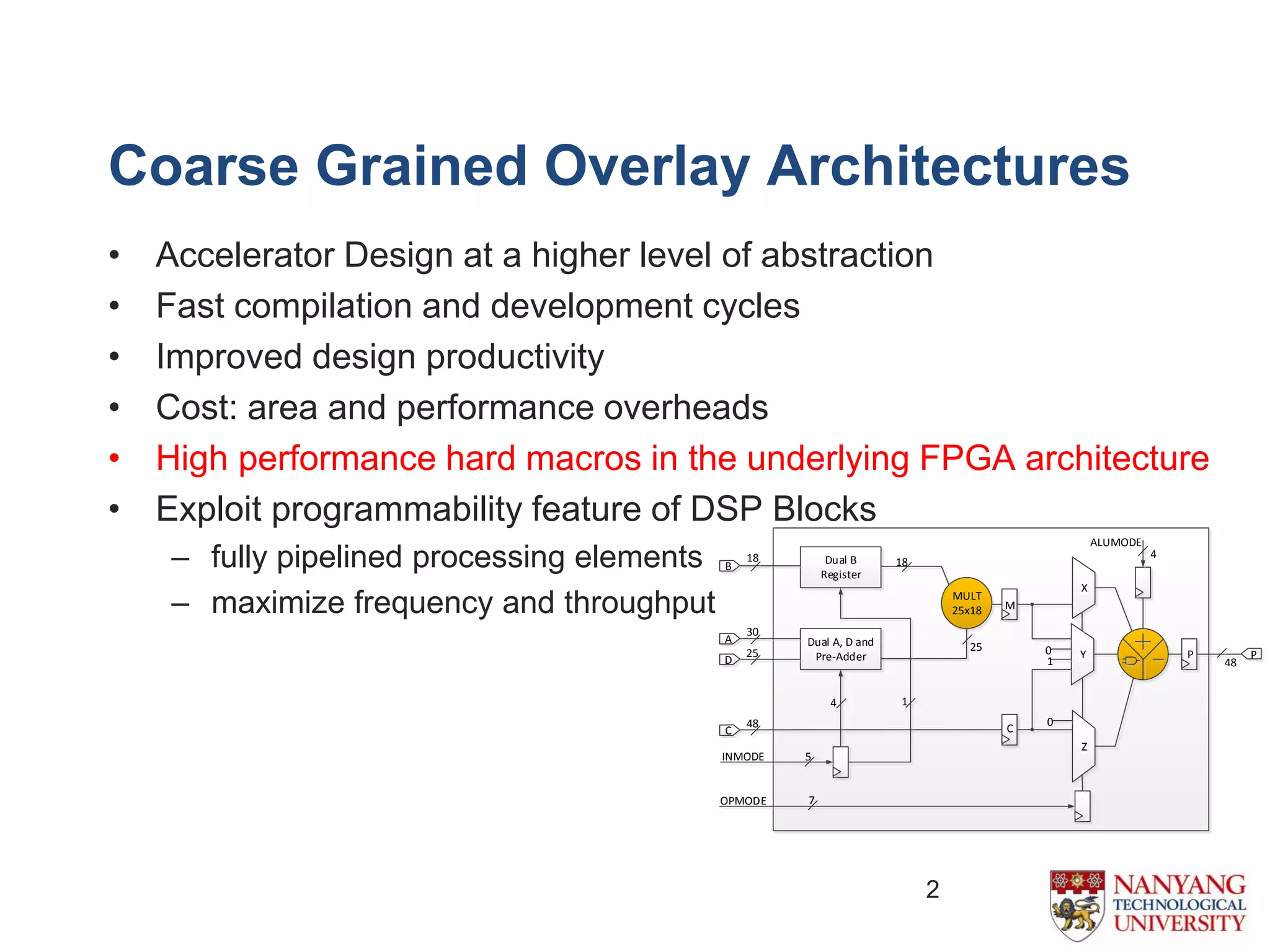
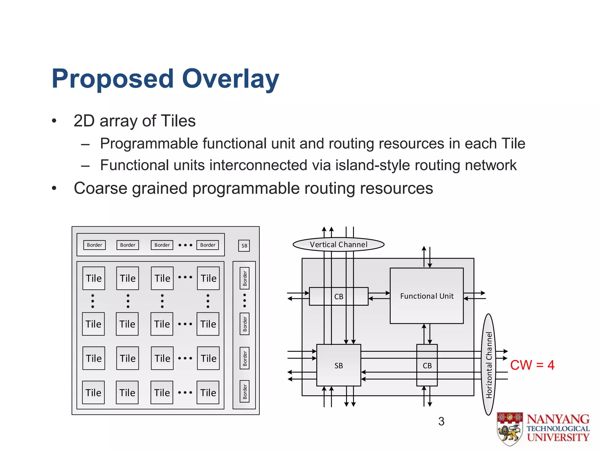
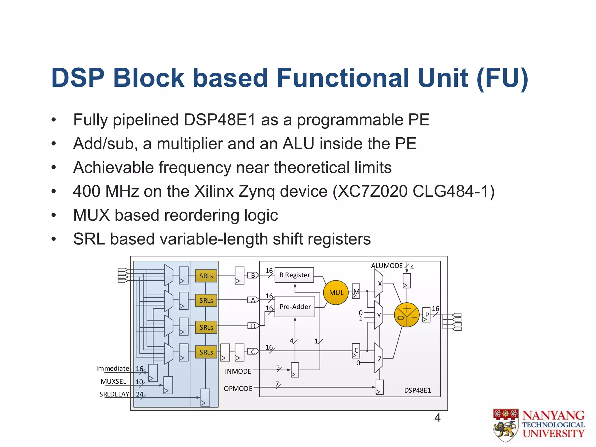
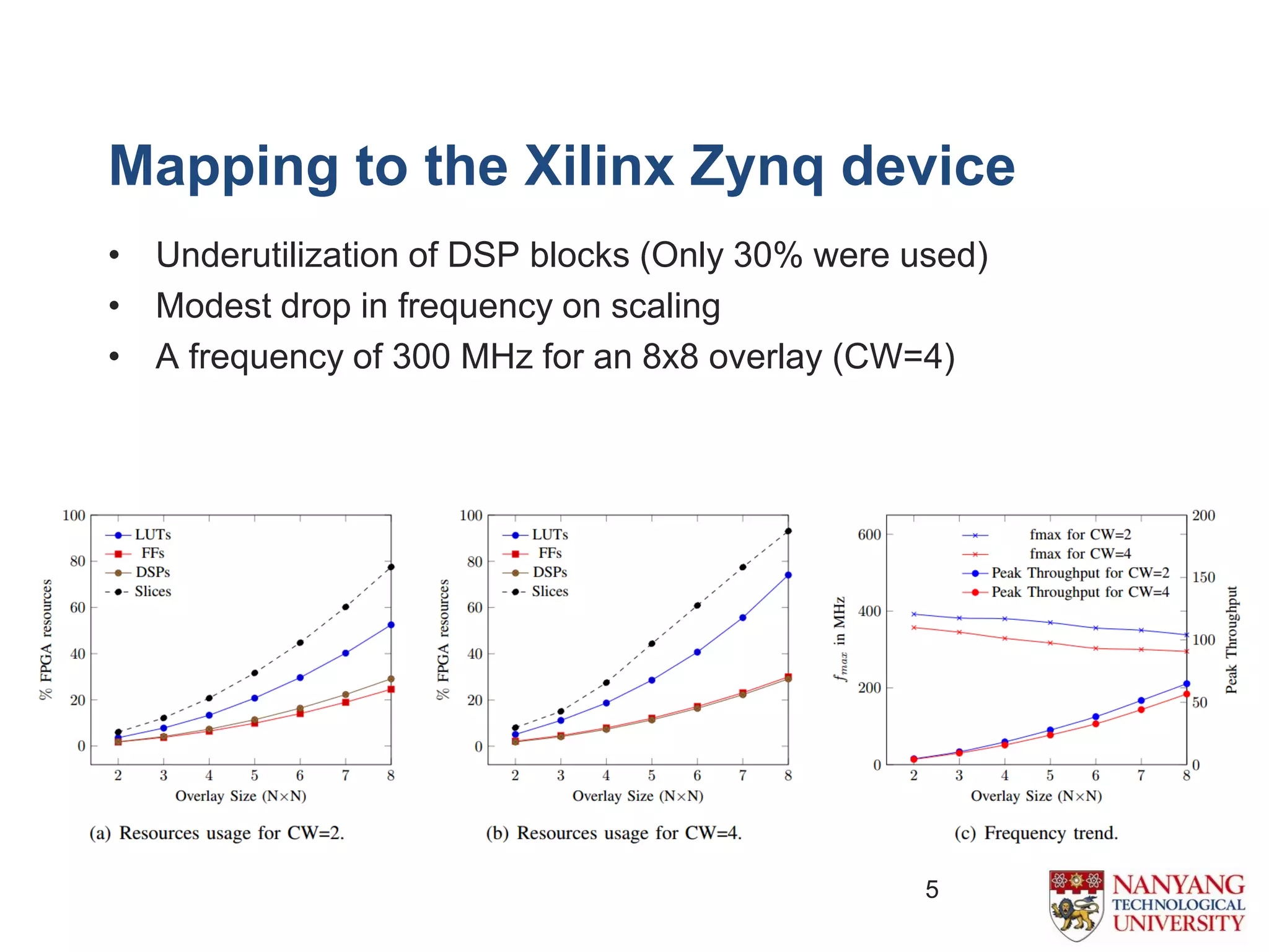
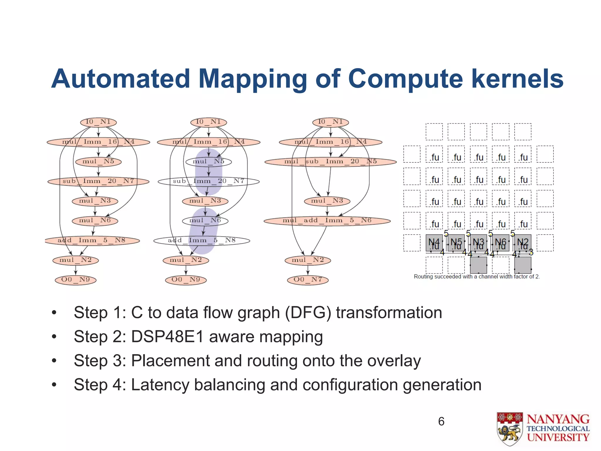
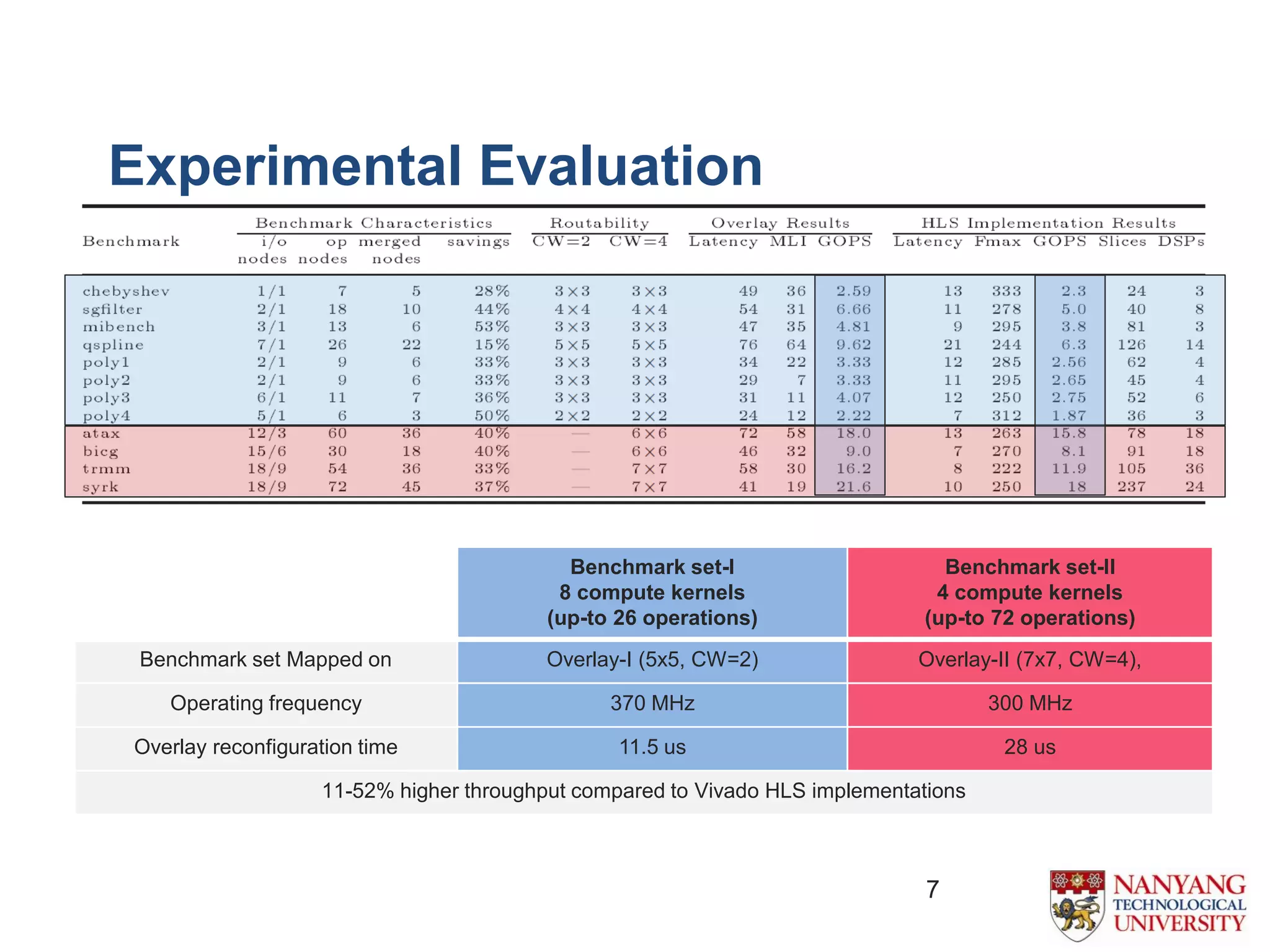

The document proposes an efficient coarse-grained overlay architecture based on DSP blocks in FPGAs. It consists of a 2D array of tiles with a programmable functional unit and routing resources in each tile. The functional unit is implemented using the fully pipelined DSP48E1 block from Xilinx FPGAs to achieve high frequencies near 400MHz. Experimental results show the overlay can map compute kernels with up to 72 operations and achieves 11-52% higher throughput than Vivado HLS implementations. Future work includes reducing the overlay area and exploring alternative interconnect architectures.