Electronic System DesignLab Manual IV Sem, B.E
Dept of E&C, MIT, Manipal Page 1
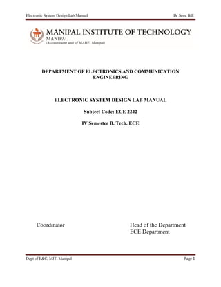
DEPARTMENT OF ELECTRONICS AND COMMUNICATION
ENGINEERING
ELECTRONIC SYSTEM DESIGN LAB MANUAL
Subject Code: ECE 2242
IV Semester B. Tech. ECE
Coordinator Head of the Department
ECE Department
2.
Electronic System DesignLab Manual IV Sem, B.E
Dept of E&C, MIT, Manipal Page 2
List of Experiments
Sl.No. Name of the Experiment
01 IC Voltage And Current Regulators
02 IC 555 Timer Applications
03 Mathematical Operations Using OPAMP
04 Precision Rectifiers Using OPAMP
05 Non-Linear Applications Of OPAMP-I
06 Non-Linear Applications Of OPAMP-II
07 Active Filters Using OPAMP-I
08 Active Filters Using OPAMP-II
09 Digital Filter Design using LabVIEW
10 PCB Design using EDA Tools
3.
Electronic System DesignLab Manual IV Sem, B.E
Dept of E&C, MIT, Manipal Page 3
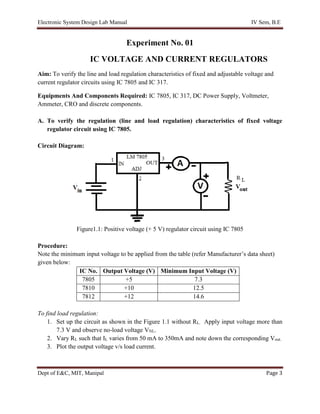
Experiment No. 01
IC VOLTAGE AND CURRENT REGULATORS
Aim: To verify the line and load regulation characteristics of fixed and adjustable voltage and
current regulator circuits using IC 7805 and IC 317.
Equipments And Components Required: IC 7805, IC 317, DC Power Supply, Voltmeter,
Ammeter, CRO and discrete components.
A. To verify the regulation (line and load regulation) characteristics of fixed voltage
regulator circuit using IC 7805.
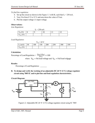
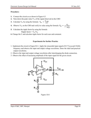
Circuit Diagram:
Figure1.1: Positive voltage (+ 5 V) regulator circuit using IC 7805
Procedure:
Note the minimum input voltage to be applied from the table (refer Manufacturer’s data sheet)
given below:
IC No. Output Voltage (V) Minimum Input Voltage (V)
7805 +5 7.3
7810 +10 12.5
7812 +12 14.6
To find load regulation:
1. Set up the circuit as shown in the Figure 1.1 without RL. Apply input voltage more than
7.3 V and observe no-load voltage VNL.
2. Vary RL such that IL varies from 50 mA to 350mA and note down the corresponding Vout.
3. Plot the output voltage v/s load current.
4.
Electronic System DesignLab Manual IV Sem, B.E
Dept of E&C, MIT, Manipal Page 4
To find line regulation:
4. Set up the circuit as shown in the Figure 1.1 with RL such that IL = 250 mA.
5. Vary Vin from 8 V to 12 V and note down the value of Vout.
6. Plot the output voltage v/s input voltage.
Observations:
Line Regulation:
IL = 250 mA
Vin (V) 8 9 10 11 12
Vout (V)
Load Regulation:
Vin = 10 V
IL (mA) 50 100 150 200 250 300 350
Vout (V)
Calculation:
Percentage of Load Regulation =
|VNL|−|VFL|
|VFL|
× 100
where VNL = No load voltage and VFL = Full load volgage
Results:
Percentage of Load Regulation: _______
B. To design and verify the working of an adjustable DC (8/ 9/ 12 V) voltage regulator
circuit using 7805 IC and to plot line and load regulation characteristics.
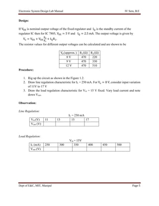
Circuit Diagram:
Figure1.2: Adjustable DC (8/ 9/ 12 V) voltage regulator circuit using IC 7805
5.
Electronic System DesignLab Manual IV Sem, B.E
Dept of E&C, MIT, Manipal Page 5
Design:
If VXX is nominal output voltage of the fixed regulator and IQ is the standby current of the
regulator IC then for IC 7805, VXX = 5 V and IQ = 2.5 mA. The output voltage is given by
Vo = VXX + VXX
R2
R1
+ IQR2.
The resistor values for different output voltages can be calculated and are shown to be
Vo(approx. ) R1(Ω) R2(Ω)
8 V 470 220
9 V 470 330
12 V 470 510
Procedure:
1. Rig up the circuit as shown in the Figure 1.2.
2. Draw line regulation characteristic for IL = 250 mA. For Vo = 8 V, consider input variation
of 11V to 17 V
3. Draw the load regulation characteristic for Vin = 15 V fixed. Vary load current and note
down Vout.
Observation:
Line Regulation:
IL = 250 mA
Vin (V) 11 13 15 17
Vout (V)
Load Regulation:
Vin = 15V
IL (mA) 250 300 350 400 450 500
Vout (V)
6.
Electronic System DesignLab Manual IV Sem, B.E
Dept of E&C, MIT, Manipal Page 6
C. To build a constant current regulator using 7805 IC and verify the regulation
characteristics.
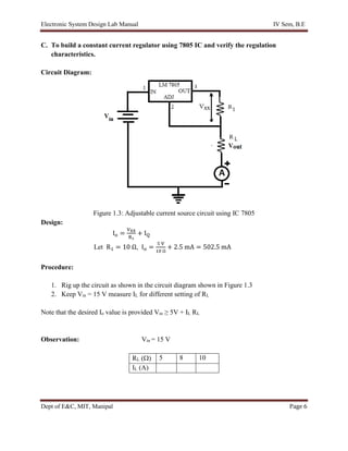
Circuit Diagram:
Figure 1.3: Adjustable current source circuit using IC 7805
Design:
Io =
VXX
R1
+ IQ
Let R1 = 10 Ω, Io =
5 V
10 Ω
+ 2.5 mA = 502.5 mA
Procedure:
1. Rig up the circuit as shown in the circuit diagram shown in Figure 1.3
2. Keep Vin = 15 V measure IL for different setting of RL
Note that the desired Io value is provided Vin ≥ 5V + IL RL
Observation: Vin = 15 V
RL () 5 8 10
IL (A)
7.
Electronic System DesignLab Manual IV Sem, B.E
Dept of E&C, MIT, Manipal Page 7
D. To design and verify the working of an adjustable voltage regulator using IC LM 317.
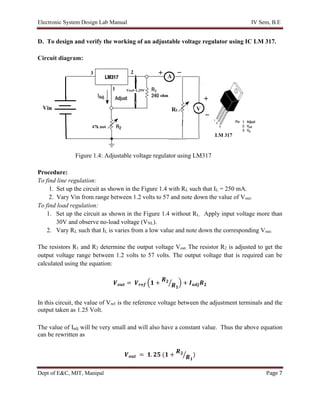
Circuit diagram:
Figure 1.4: Adjustable voltage regulator using LM317
Procedure:
To find line regulation:
1. Set up the circuit as shown in the Figure 1.4 with RL such that IL = 250 mA.
2. Vary Vin from range between 1.2 volts to 57 and note down the value of Vout.
To find load regulation:
1. Set up the circuit as shown in the Figure 1.4 without RL. Apply input voltage more than
30V and observe no-load voltage (VNL).
2. Vary RL such that IL is varies from a low value and note down the corresponding Vout.
The resistors R1 and R2 determine the output voltage Vout. The resistor R2 is adjusted to get the
output voltage range between 1.2 volts to 57 volts. The output voltage that is required can be
calculated using the equation:
𝑽𝒐𝒖𝒕 = 𝑽𝒓𝒆𝒇 (𝟏 +
𝑹𝟐
𝑹𝟏
⁄ ) + 𝑰𝒂𝒅𝒋𝑹𝟐
In this circuit, the value of Vref is the reference voltage between the adjustment terminals and the
output taken as 1.25 Volt.
The value of Iadj will be very small and will also have a constant value. Thus the above equation
can be rewritten as
𝑽𝒐𝒖𝒕 = 𝟏. 𝟐𝟓 (𝟏 +
𝑹𝟐
𝑹𝟏
⁄ )
8.
Electronic System DesignLab Manual IV Sem, B.E
Dept of E&C, MIT, Manipal Page 8
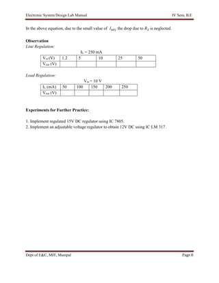
In the above equation, due to the small value of 𝐼𝑎𝑑𝑗 the drop due to 𝑅2 is neglected.
Observation
Line Regulation:
IL = 250 mA
Vin (V) 1.2 5 10 25 50
Vout (V)
Load Regulation:
Vin = 10 V
IL (mA) 50 100 150 200 250
Vout (V)
Experiments for Further Practice:
1. Implement regulated 15V DC regulator using IC 7805.
2. Implement an adjustable voltage regulator to obtain 12V DC using IC LM 317.
9.
Electronic System DesignLab Manual IV Sem, B.E
Dept of E&C, MIT, Manipal Page 9
Experiment No. 02
IC 555 TIMER APPLICATIONS
Aim: To design Astable and Monostable multivibrators using IC 555.
Equipments and Components Required: IC 555, DC Power Supply, CRO, discrete
components.
Procedure:
1. Connect the circuit as shown in the circuit diagram.
2. Observe the output waveform at pin 3 of IC 555 on the CRO.
3. Also observe the voltage across the Capacitor at pin 2.
4. Use VCC of 5 Volt DC.
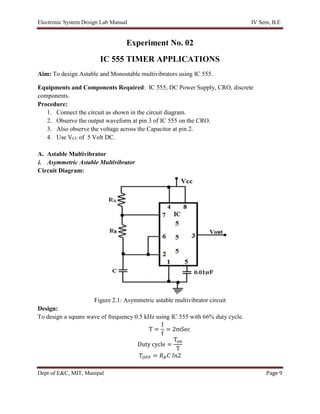
A. Astable Multivibrator
i. Asymmetric Astable Multivibrator
Circuit Diagram:
Figure 2.1: Asymmetric astable multivibrator circuit
Design:
To design a square wave of frequency 0.5 kHz using IC 555 with 66% duty cycle.
T =
1
f
= 2mSec
Duty cycle =
Ton
T
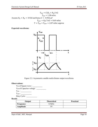
𝑇𝑂𝐹𝐹 = 𝑅𝐵𝐶 𝑙𝑛2
Electronic System DesignLab Manual IV Sem, B.E
Dept of E&C, MIT, Manipal Page 11
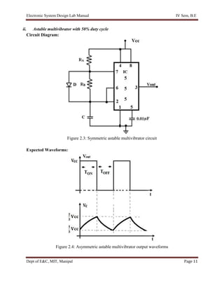
ii. Astable multivibrator with 50% duty cycle
Circuit Diagram:
Figure 2.3: Symmetric astable multivibrator circuit
Expected Waveforms:
Figure 2.4: Asymmetric astable multivibrator output waveforms
12.
Electronic System DesignLab Manual IV Sem, B.E
Dept of E&C, MIT, Manipal Page 12
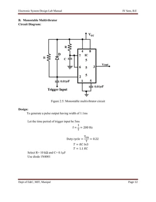
B. Monostable Multivibrator
Circuit Diagram:
Figure 2.5: Monostable multivibrator circuit
Design:
To generate a pulse output having width of 1.1ms
Let the time period of trigger input be 5ms
f =
1
T
= 200 Hz
Duty cycle =
TON
T
= 0.22
𝑇 = 𝑅𝐶 𝑙𝑛3
𝑇 = 1.1 𝑅𝐶
Select R= 10 kΩ and C= 0.1µF
Use diode 1N4001
13.
Electronic System DesignLab Manual IV Sem, B.E
Dept of E&C, MIT, Manipal Page 13
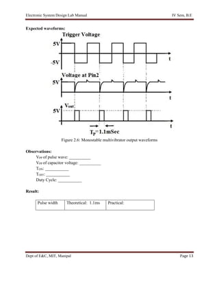
Expected waveforms:
Figure 2.6: Monostable multivibrator output waveforms
Observations:
VPP of pulse wave: __________
VPP of capacitor voltage: __________
TON: ___________
TOFF: ___________
Duty Cycle: ___________
Result:
Pulse width Theoretical: 1.1ms Practical:
14.
Electronic System DesignLab Manual IV Sem, B.E
Dept of E&C, MIT, Manipal Page 14
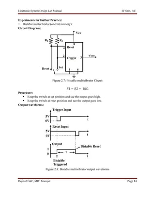
Experiments for further Practice:
1. Bistable multivibrator (one bit memory).
Circuit Diagram:
Figure 2.7: Bistable multivibrator Circuit
𝑅1 = 𝑅2 = 1𝐾Ω
Procedure:
Keep the switch at set position and see the output goes high.
Keep the switch at reset position and see the output goes low.
Output waveforms:
Figure 2.8: Bistable multivibrator output waveforms
15.
Electronic System DesignLab Manual IV Sem, B.E
Dept of E&C, MIT, Manipal Page 15
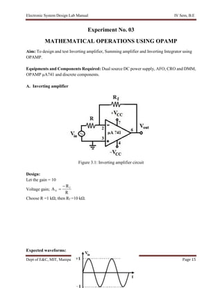
Experiment No. 03
MATHEMATICAL OPERATIONS USING OPAMP
Aim: To design and test Inverting amplifier, Summing amplifier and Inverting Integrator using
OPAMP.
Equipments and Components Required: Dual source DC power supply, AFO, CRO and DMM,
OPAMP μA741 and discrete components.
A. Inverting amplifier
Figure 3.1: Inverting amplifier circuit
Design:
Let the gain = 10
Voltage gain;
R
R
A f
V
Choose R =1 kΩ, then Rf =10 kΩ.
Expected waveforms:
16.
Electronic System DesignLab Manual IV Sem, B.E
Dept of E&C, MIT, Manipal Page 16
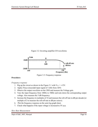
Figure 3.2: Inverting amplifier I/O waveforms
Figure 3.3: Frequency response
Procedure:
Frequency response
1. Rig up the circuit as shown in the Figure 3.1 with VCC = ±12V.
2. Apply 2Vp-p sinusoidal input signal of 1 kHz from AFO.
3. Observe the output waveform on the CRO and measure the Voltage gain.
4. Vary the input frequency from 100Hz to 1MHz and note down the corresponding output
voltage. Also measure the 3 dB frequency.
5. Increase the frequency in multiples of 10 and measure the roll-off rate in dB per decade (or
multiple of 2 to measure the roll-off rate in dB per octave).
6. Plot the frequency response on the semi-log graph sheet.
7. Check what happens if the input voltage is increased to 5V p-p.
Slew Rate Measurement
17.
Electronic System DesignLab Manual IV Sem, B.E
Dept of E&C, MIT, Manipal Page 17
8. Apply square wave signal of frequency 10 kHz and peak to peak amplitude 0.5V (such that
it operates in mid-band and linear region) to the inverting amplifier shown in Figure 3.1
9. Observe the input and output waveforms and the transitions between two levels of square
wave. The slope measured at the transitions gives slew rate of OPAMP.
10. Change the frequency of the signal and plot the input and output waveform properly
labelled.
Observations:
Table 3.1: Frequency response estimation
Input signal = 0.5V (p-p)
Frequency (Hz) Output Voltage(Vout) Gain (Vout/Vin) Gain in dB
20 log(Vout/Vin)
Table 3.2 :Slew Rate measurement
Frequency Slope (V/μsec)
5 kHz
10 kHz
20 Hz
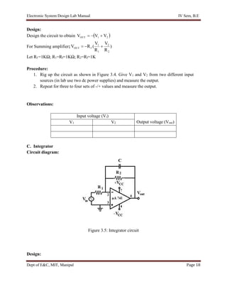
B. Summing Amplifier
Circuit diagram:
Figure 3.4: Summing amplifier circuit
18.
Electronic System DesignLab Manual IV Sem, B.E
Dept of E&C, MIT, Manipal Page 18
Design:
Design the circuit to obtain
2
1
OUT V
V
V
For Summing amplifier; )
R
V
R
V
(
R
V
2
2
1
1
f
OUT
Let Rf =1KΩ; R1=Rf=1KΩ; R2=Rf=1K
Procedure:
1. Rig up the circuit as shown in Figure 3.4. Give V1 and V2 from two different input
sources (in lab use two dc power supplies) and measure the output.
2. Repeat for three to four sets of -/+ values and measure the output.
Observations:
Input voltage (Vi)
Output voltage (Vout)
V1 V2
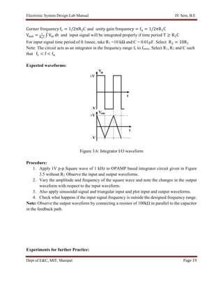
C. Integrator
Circuit diagram:
Figure 3.5: Integrator circuit
Design:
19.
Electronic System DesignLab Manual IV Sem, B.E
Dept of E&C, MIT, Manipal Page 19
Corner frequency fc = 1/2πR2C and unity gain frequency = fu = 1/2πR1C
Vout = 1
R1C
∫ Vin dt and input signal will be integrated properly if time period T ≥ R1C
For input signal time period of 0.1msec, take R1 =10 kΩ and C = 0.01µF. Select R2 = 10R1
Note: The circuit acts as an integrator in the frequency range fc to funity. Select R1, R2 and C such
that fc < f < fu
Expected waveforms:
Figure 3.6: Integrator I/O waveform
Procedure:
1. Apply 1V p-p Square wave of 1 kHz to OPAMP based integrator circuit given in Figure
3.5 without R2. Observe the input and output waveforms.
2. Vary the amplitude and frequency of the square wave and note the changes in the output
waveform with respect to the input waveform.
3. Also apply sinusoidal signal and triangular input and plot input and output waveforms.
4. Check what happens if the input signal frequency is outside the designed frequency range.
Note: Observe the output waveform by connecting a resistor of 100kΩ in parallel to the capacitor
in the feedback path.
Experiments for further Practice:
20.
Electronic System DesignLab Manual IV Sem, B.E
Dept of E&C, MIT, Manipal Page 20
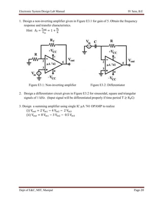
1. Design a non-inverting amplifier given in Figure E3.1 for gain of 5. Obtain the frequency
response and transfer characteristics.
Hint: Af =
Vout
Vin
= 1 +
Rf
R
Figure E3.1: Non-inverting amplifier Figure E3.2: Differentiator
2. Design a differentiator circuit given in Figure E3.2 for sinusoidal, square and triangular
signals of 1 kHz. (Input signal will be differentiated properly if time period T ≥ RFC)
3. Design a summing amplifier using single IC μA 741 OPAMP to realize
(i) Vout = 2 Vin1 − 4 Vin2 − 2 Vin3
(ii) Vout = 8 Vin1 − 3 Vin2 − 0.5 Vin3
21.
Electronic System DesignLab Manual IV Sem, B.E
Dept of E&C, MIT, Manipal Page 21
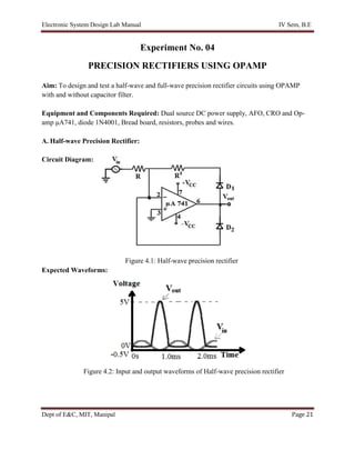
Experiment No. 04
PRECISION RECTIFIERS USING OPAMP
Aim: To design and test a half-wave and full-wave precision rectifier circuits using OPAMP
with and without capacitor filter.
Equipment and Components Required: Dual source DC power supply, AFO, CRO and Op-
amp μA741, diode 1N4001, Bread board, resistors, probes and wires.
A. Half-wave Precision Rectifier:
Circuit Diagram:
Figure 4.1: Half-wave precision rectifier
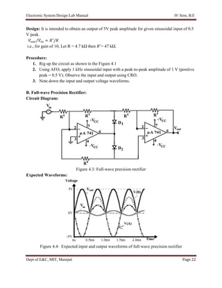
Expected Waveforms:
Figure 4.2: Input and output waveforms of Half-wave precision rectifier
22.
Electronic System DesignLab Manual IV Sem, B.E
Dept of E&C, MIT, Manipal Page 22
Design: It is intended to obtain an output of 5V peak amplitude for given sinusoidal input of 0.5
V peak.
𝑉𝑜𝑢𝑡 𝑉𝑖𝑛
⁄ = 𝑅′
/𝑅
i.e., for gain of 10, Let R = 4.7 kΩ then 𝑅′
= 47 kΩ.
Procedure:
1. Rig up the circuit as shown in the Figure 4.1
2. Using AFO, apply 1 kHz sinusoidal input with a peak-to-peak amplitude of 1 V (positive
peak = 0.5 V). Observe the input and output using CRO.
3. Note down the input and output voltage waveforms.
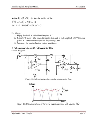
B. Full-wave Precision Rectifier:
Circuit Diagram:
Figure 4.3: Full-wave precision rectifier
Expected Waveforms:
Figure 4.4: Expected input and output waveforms of full-wave precision rectifier
23.
Electronic System DesignLab Manual IV Sem, B.E
Dept of E&C, MIT, Manipal Page 23
Design: in
P V
R
R
V )
( '
. Let VP = 5V and Vin = 0.5V.
10
5
.
0
5
'
in
P V
V
R
R
Let R = 4.7 kΩ then R’ = 10R = 47 kΩ.
Procedure:
1. Rig up the circuit as shown in the Figure 4.3.
2. Using AFO, apply 1 kHz sinusoidal input with a peak-to-peak amplitude of 1 V (positive
peak = 0.5 V). Observe the input and output using CRO.
3. Note down the input and output voltage waveforms.
C. Full-wave precision rectifier with capacitor filter
Circuit Diagram:
Figure 4.5: Full-wave precision rectifier with capacitor filter
Figure 4.6: Output waveforms of full-wave precision rectifier with capacitor filter
24.
Electronic System DesignLab Manual IV Sem, B.E
Dept of E&C, MIT, Manipal Page 24
Procedure:
1. Connect the circuit as as shown in Figure 4.5.
2. Note down the peak value V׳m of the signal observed on the CRO
3. Calculate Vac by using the formula: Vac =
Vr−pp
2√3
4. Observe Vdc on the CRO and verify its value using the formula: Vdc =
Vm
′
1 +
1
4fRLC
5. Calculate the ripple factor by using the formula
Ripple factor = Vac/Vdc
6. Change the C and calculate ripple factor for each case and comment.
Experiments for further Practice
1. Implement the circuit in Figure E4.1. Apply the sinusoidal input signal of 0.5 V p-p and 10 kHz
frequency and observe the input and output voltage waveforms. Draw the ideal and practical
output waveforms.
2. Observe the input and output voltage waveforms after interchanging the diode connection.
3. Observe the effect of increasing amplitude of the input signal for the given circuit.
Figure: E4.1
25.
Electronic System DesignLab Manual IV Sem, B.E
Dept of E&C, MIT, Manipal Page 25
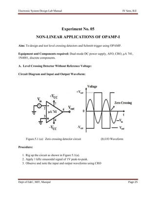
Experiment No. 05
NON-LINEAR APPLICATIONS OF OPAMP-I
Aim: To design and test level crossing detectors and Schmitt trigger using OPAMP.
Equipment and Components required: Dual-mode DC power supply, AFO, CRO, µA 741,
1N4001, discrete components.
A. Level Crossing Detector Without Reference Voltage:
Circuit Diagram and Input and Output Waveform:
Figure.5.1 (a): Zero crossing detector circuit (b) I/O Waveform
Procedure:
1. Rig up the circuit as shown in Figure 5.1(a).
2. Apply 1 kHz sinusoidal signal of 1V peak-to-peak.
3. Observe and note the input and output waveforms using CRO
26.
Electronic System DesignLab Manual IV Sem, B.E
Dept of E&C, MIT, Manipal Page 26
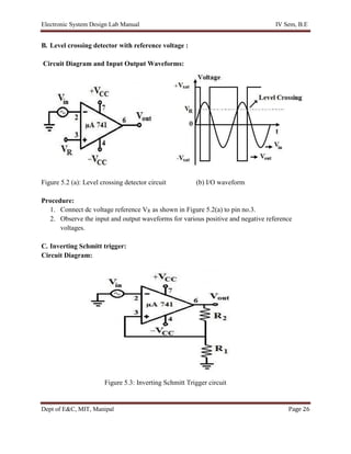
B. Level crossing detector with reference voltage :
Circuit Diagram and Input Output Waveforms:
Figure 5.2 (a): Level crossing detector circuit (b) I/O waveform
Procedure:
1. Connect dc voltage reference VR as shown in Figure 5.2(a) to pin no.3.
2. Observe the input and output waveforms for various positive and negative reference
voltages.
C. Inverting Schmitt trigger:
Circuit Diagram:
Figure 5.3: Inverting Schmitt Trigger circuit
27.
Electronic System DesignLab Manual IV Sem, B.E
Dept of E&C, MIT, Manipal Page 27
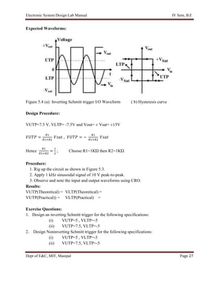
Expected Waveforms:
Figure 5.4 (a): Inverting Schmitt trigger I/O Waveform ( b) Hysteresis curve
Design Procedure:
VUTP=7.5 V, VLTP= -7.5V and Vout= ± Vsat= ±15V
𝑉𝑈𝑇𝑃 =
𝑅1
𝑅1+𝑅2
𝑉𝑠𝑎𝑡 , 𝑉𝑈𝑇𝑃 = −
𝑅1
𝑅1+𝑅2
𝑉𝑠𝑎𝑡
Hence
𝑅1
𝑅1+𝑅2
=
1
2
; Choose R1=1KΏ then R2=1KΏ
Procedure:
1. Rig up the circuit as shown in Figure 5.3.
2. Apply 1 kHz sinusoidal signal of 10 V peak-to-peak.
3. Observe and note the input and output waveforms using CRO.
Results:
VUTP(Theoretical) = VLTP(Theoretical) =
VUTP(Practical)) = VLTP(Practical) =
Exercise Questions:
1. Design an inverting Schmitt trigger for the following specifications:
(i) VUTP=5 , VLTP=-5
(ii) VUTP=7.5, VLTP=-5
2. Design Noninverting Schmitt trigger for the following specifications:
(i) VUTP=5 , VLTP=-5
(ii) VUTP=7.5, VLTP=-5
28.
Electronic System DesignLab Manual IV Sem, B.E
Dept of E&C, MIT, Manipal Page 28
Experiment- 6
NON-LINEAR APPLICATIONS OF OPAMP - II
Aim: To design and practically verify Square wave generator and Monostable multivibrator
using Operational Amplifier.
Equipments and Components Required: Dual-mode DC power supply, AFO, CRO, µA-741,
1N4001, resistors and capacitors.
A. Square wave generator (Astable Multivibrator):
Specifications:
Frequency = 4.5 kHz
Amplitude = ±12V
Circuit Diagram:
Figure 6.1: Astable multivibrator circuit Figure.6.2: Astable multivibrator Output
Design:
The period of the square wave is given by T = 2 RC ln {
(1+β)
(1−β)
} ------ (1)
where β = [
𝑅2
𝑅1+𝑅2
] ------ (2)
Assuming 𝐑𝟏 = 𝐑𝟐 = 𝟏𝟎𝐤Ω, β= 0.5 [ from equation (2) ]
Period of the square wave: T= 2 RC ln (3) = 2.2 RC [from equation (1)] ------ (3)
Also, from the specifications given, T =
1
f
=
1
4.5 kHz
= 0.22 msec
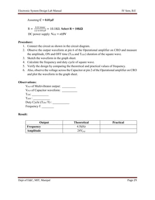
29.
Electronic System DesignLab Manual IV Sem, B.E
Dept of E&C, MIT, Manipal Page 29
Assumng C = 0.01µF
R =
0.22 msec
2.2 x 0.01µF
= 10.1KΩ. Select R = 10KΩ
DC power supply: VCC = ±13V
Procedure:
1. Connect the circuit as shown in the circuit diagram.
2. Observe the output waveform at pin 6 of the Operational amplifier on CRO and measure
the amplitude, ON and OFF time (TON and TOFF) duration of the square wave.
3. Sketch the waveform in the graph sheet.
4. Calculate the frequency and duty cycle of square wave.
5. Verify the design by comparing the theoretical and practical values of frequency.
6. Also, observe the voltage across the Capacitor at pin 2 of the Operational amplifier on CRO
and plot the waveform in the graph sheet.
Observations:
VP-P of Multivibrator output: _________
VP-P of Capacitor waveform: __________
TON: ___________
TOFF : ___________
Duty Cycle (TON /T) : ___________
Frequency f: ________
Result:
Output Theoretical Practical
Frequency 4.5kHz
Amplitude 24Vp-p
30.
Electronic System DesignLab Manual IV Sem, B.E
Dept of E&C, MIT, Manipal Page 30
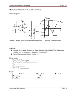
6.2 Astable multivibrator with amplitude Limiter:
Circuit Diagram:
Figure 6.3: Astable multivibrator with amplitude limiter Figure 6.4: Output waveform
Procedure:
1. Connect the circuit as shown in the circuit diagram (Zener diode of 6.3V breakdown
voltage) with the component values given in Section 6.1.
2. Repeat the procedure given in Section 6.1.
Observations:
VPP of Multivibrator output :__________
VPP of capacitor waveform : __________
TON : ___________
TOFF : ___________
Duty Cycle : ___________
Result:
Output Theoretical Practical
Frequency 4.5kHz
Amplitude 12.6Vp-p
31.
Electronic System DesignLab Manual IV Sem, B.E
Dept of E&C, MIT, Manipal Page 31
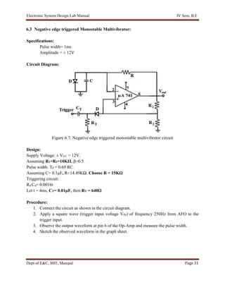
6.3 Negative edge triggered Monostable Multivibrator:
Specifications:
Pulse width= 1ms
Amplitude = ± 12V
Circuit Diagram:
Figure 6.7: Negative edge triggered monostable multivibrator circuit
Design:
Supply Voltage: ± VCC = 12V.
Assuming R1=R2=10KΩ, β=0.5.
Pulse width: TP = 0.69 RC.
Assuming C= 0.1μF, R=14.49KΩ. Choose R = 15KΩ
Triggering circuit:
Rd Cd= 0.0016t
Let t = 4ms, CT= 0.01μF, then RT = 640Ω
Procedure:
1. Connect the circuit as shown in the circuit diagram.
2. Apply a square wave (trigger input voltage VIN) of frequency 250Hz from AFO to the
trigger input.
3. Observe the output waveform at pin 6 of the Op-Amp and measure the pulse width.
4. Sketch the observed waveform in the graph sheet.
32.
Electronic System DesignLab Manual IV Sem, B.E
Dept of E&C, MIT, Manipal Page 32
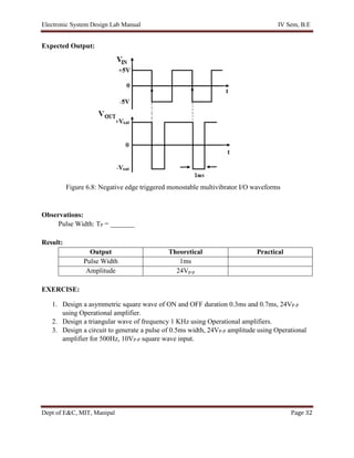
Expected Output:
Figure 6.8: Negative edge triggered monostable multivibrator I/O waveforms
Observations:
Pulse Width: TP = _______
Result:
Output Theoretical Practical
Pulse Width 1ms
Amplitude 24Vp-p
EXERCISE:
1. Design a asymmetric square wave of ON and OFF duration 0.3ms and 0.7ms, 24VP-P
using Operational amplifier.
2. Design a triangular wave of frequency 1 KHz using Operational amplifiers.
3. Design a circuit to generate a pulse of 0.5ms width, 24VP-P amplitude using Operational
amplifier for 500Hz, 10VP-P square wave input.
33.
Electronic System DesignLab Manual IV Sem, B.E
Dept of E&C, MIT, Manipal Page 33
Experiment No. 07
ACTIVE FILTERS USING OPAMP-I
Aim: To design and implement Low pass and High pass active filters. Observe and plot the
frequency responses.
Equipment and Components Required: Dual source DC power supply, AFO, CRO and
OPAMP μA741 & discrete components.
A. Low Pass Filter (LPF):
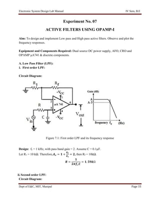
i. First order LPF:
Circuit Diagram:
Figure 7.1: First order LPF and its frequency response
Design: fc = 1 kHz, with pass band gain = 2. Assume C = 0.1µF.
Let R1 = 10 kΩ. Therefore,𝑨𝒗 = 𝟏 +
𝑹𝒇
𝑹𝟏
= 𝟐, then Rf = 10kΩ.
𝑹 =
𝟏
𝟐𝝅𝒇𝒄𝑪
= 𝟏. 𝟓𝟗𝒌Ω
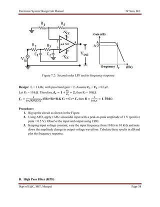
ii.Second order LPF:
Circuit Diagram:
34.
Electronic System DesignLab Manual IV Sem, B.E
Dept of E&C, MIT, Manipal Page 34
Design: fc = 1 kHz, with pass band gain = 2. Assume 𝑪𝟏 = 𝑪𝟐 = 0.1µF.
Let R1 = 10 kΩ. Therefore,𝑨𝒗 = 𝟏 +
𝑹𝒇
𝑹𝟏
= 𝟐, then Rf = 10kΩ.
𝒇𝒄 =
𝟏
𝟐𝝅√𝑹𝟐𝑹𝟑𝑪𝟏𝑪𝟐
, if R2=R3=R & C1 = C2 = C, then 𝑹 =
𝟏
𝟐𝝅𝒇𝒄𝑪
= 𝟏. 𝟓𝟗𝒌Ω
Procedure:
1. Rig up the circuit as shown in the Figure.
2. Using AFO, apply 1 kHz sinusoidal input with a peak-to-peak amplitude of 1 V (positive
peak = 0.5 V). Observe the input and output using CRO.
3. Keeping input voltage constant, vary the input frequency from 10 Hz to 10 kHz and note
down the amplitude change in output voltage waveform. Tabulate these results in dB and
plot the frequency response.
B. High Pass Filter (HPF)
Figure 7.2: Second order LPF and its frequency response
35.
Electronic System DesignLab Manual IV Sem, B.E
Dept of E&C, MIT, Manipal Page 35
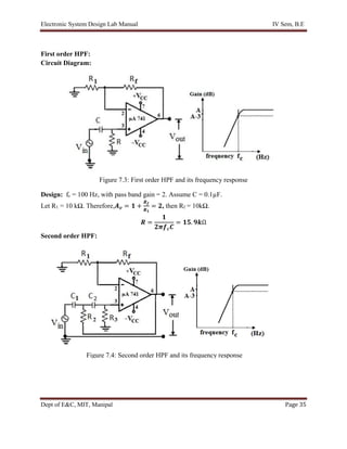
First order HPF:
Circuit Diagram:
Figure 7.3: First order HPF and its frequency response
Design: fc = 100 Hz, with pass band gain = 2. Assume C = 0.1µF.
Let R1 = 10 kΩ. Therefore,𝑨𝒗 = 𝟏 +
𝑹𝒇
𝑹𝟏
= 𝟐, then Rf = 10kΩ.
𝑹 =
𝟏
𝟐𝝅𝒇𝒄𝑪
= 𝟏𝟓. 𝟗𝒌Ω
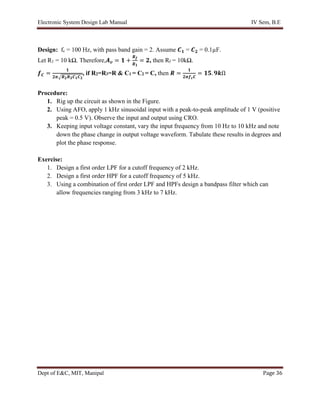
Second order HPF:
Figure 7.4: Second order HPF and its frequency response
36.
Electronic System DesignLab Manual IV Sem, B.E
Dept of E&C, MIT, Manipal Page 36
Design: fc = 100 Hz, with pass band gain = 2. Assume 𝑪𝟏 = 𝑪𝟐 = 0.1µF.
Let R1 = 10 kΩ. Therefore,𝑨𝒗 = 𝟏 +
𝑹𝒇
𝑹𝟏
= 𝟐, then Rf = 10kΩ.
𝒇𝑪 =
𝟏
𝟐𝝅√𝑹𝟐𝑹𝟑𝑪𝟏𝑪𝟐
, if R2=R3=R & C1 = C2 = C, then 𝑹 =
𝟏
𝟐𝝅𝒇𝒄𝑪
= 𝟏𝟓. 𝟗𝒌Ω
Procedure:
1. Rig up the circuit as shown in the Figure.
2. Using AFO, apply 1 kHz sinusoidal input with a peak-to-peak amplitude of 1 V (positive
peak = 0.5 V). Observe the input and output using CRO.
3. Keeping input voltage constant, vary the input frequency from 10 Hz to 10 kHz and note
down the phase change in output voltage waveform. Tabulate these results in degrees and
plot the phase response.
Exercise:
1. Design a first order LPF for a cutoff frequency of 2 kHz.
2. Design a first order HPF for a cutoff frequency of 5 kHz.
3. Using a combination of first order LPF and HPFs design a bandpass filter which can
allow frequencies ranging from 3 kHz to 7 kHz.
37.
Electronic System DesignLab Manual IV Sem, B.E
Dept of E&C, MIT, Manipal Page 37
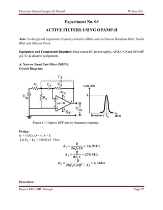
Experiment No. 08
ACTIVE FILTERS USING OPAMP-II
Aim: To design and implement frequency selective filters such as Narrow Bandpass filter, Notch
filter and All pass filters.
Equipment and Components Required: Dual source DC power supply, AFO, CRO and OPAMP
μA741 & discrete components.
A. Narrow Band Pass Filter (NBPF):
Circuit Diagram:
Design:
fC = 1 kHz, Q = 4, A = 8,
Let 𝑪𝟏 = 𝑪𝟐 = 0.0047µF. Then
𝑹𝟏 =
𝑸
𝟐𝝅𝒇𝑪𝑪𝑨
= 𝟏𝟔. 𝟗𝟑𝒌Ω
𝑹𝟑 =
𝑸
𝝅𝒇𝑪𝑪
= 𝟐𝟕𝟎. 𝟗𝒌Ω
𝑹𝟐 =
𝑸
𝟐𝝅𝒇𝑪𝑪(𝟐𝑸𝟐 − 𝑨)
= 𝟓. 𝟒𝟔𝒌Ω
Procedure:
Figure 8.1: Narrow BPF and its frequency response
38.
Electronic System DesignLab Manual IV Sem, B.E
Dept of E&C, MIT, Manipal Page 38
1. Rig up the circuit as shown in the Figure 8.1
3. Using AFO, apply 1 kHz sinusoidal input with a peak-to-peak amplitude of 1V. Observe the
input and output using CRO.
4. Keeping input voltage constant, vary the input frequency from 10 Hz to 10 kHz and note
down the amplitude change in output voltage waveform. Tabulate these results in dB and plot
the frequency response.
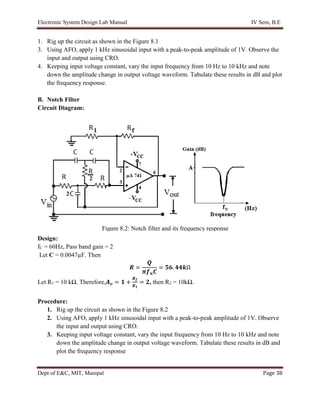
B. Notch Filter
Circuit Diagram:
Design:
fC = 60Hz, Pass band gain = 2
Let C = 0.0047µF. Then
𝑹 =
𝑸
𝝅𝒇𝒏𝑪
= 𝟓𝟔. 𝟒𝟒𝒌Ω
Let R1 = 10 kΩ. Therefore,𝑨𝒗 = 𝟏 +
𝑹𝒇
𝑹𝟏
= 𝟐, then R2 = 10kΩ.
Procedure:
1. Rig up the circuit as shown in the Figure 8.2
2. Using AFO, apply 1 kHz sinusoidal input with a peak-to-peak amplitude of 1V. Observe
the input and output using CRO.
3. Keeping input voltage constant, vary the input frequency from 10 Hz to 10 kHz and note
down the amplitude change in output voltage waveform. Tabulate these results in dB and
plot the frequency response
Figure 8.2: Notch filter and its frequency response
39.
Electronic System DesignLab Manual IV Sem, B.E
Dept of E&C, MIT, Manipal Page 39
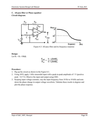
C. All pass filter or Phase equalizer
Circuit diagram:
Design:
Let Rf = R1=10kΩ,
𝑽𝒐𝒖𝒕
𝑽𝒊𝒏
=
𝟏 − 𝒋𝟐𝝅𝑹𝒇𝒄
𝟏 + 𝒋𝟐𝝅𝑹𝒇𝒄
Procedure:
1. Rig up the circuit as shown in the Figure 8.3.
2. Using AFO, apply 1 kHz sinusoidal input with a peak-to-peak amplitude of 1 V (positive
peak = 0.5 V). Observe the input and output using CRO.
3. Keeping input voltage constant, vary the input frequency from 10 Hz to 10 kHz and note
down the phase change in output voltage waveform. Tabulate these results in degrees and
plot the phase response.
Figure 8.3: All pass filter and its frequency response
40.
Electronic System DesignLab Manual IV Sem, B.E
Dept of E&C, MIT, Manipal Page 40
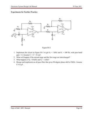
Experiments for Further Practice:
Figure E8.1
1. Implement the circuit in Figure E8.1 to get fH = 1 kHz and fL = 100 Hz, with pass band
gain = 4. Assume C = C' = 0.1µF.
2. What will happen if the second stage and the first stage are interchanged?
3. What happens if fH =10 kHz and fL = 1 kHz?
4. Design and implement an all pass filter that gives 90-degree phase shift at 5KHz. Assume
C=0.1µF.

![Electronic System Design Lab Manual IV Sem, B.E
Dept of E&C, MIT, Manipal Page 28
Experiment- 6
NON-LINEAR APPLICATIONS OF OPAMP - II
Aim: To design and practically verify Square wave generator and Monostable multivibrator
using Operational Amplifier.
Equipments and Components Required: Dual-mode DC power supply, AFO, CRO, µA-741,
1N4001, resistors and capacitors.
A. Square wave generator (Astable Multivibrator):
Specifications:
Frequency = 4.5 kHz
Amplitude = ±12V
Circuit Diagram:
Figure 6.1: Astable multivibrator circuit Figure.6.2: Astable multivibrator Output
Design:
The period of the square wave is given by T = 2 RC ln {
(1+β)
(1−β)
} ------ (1)
where β = [
𝑅2
𝑅1+𝑅2
] ------ (2)
Assuming 𝐑𝟏 = 𝐑𝟐 = 𝟏𝟎𝐤Ω, β= 0.5 [ from equation (2) ]
Period of the square wave: T= 2 RC ln (3) = 2.2 RC [from equation (1)] ------ (3)
Also, from the specifications given, T =
1
f
=
1
4.5 kHz
= 0.22 msec](https://image.slidesharecdn.com/esdlabmanual-250404060617-d997fdd2/85/Electronic-system-design-laboratory-manual-pdf-28-320.jpg)