This document summarizes the fabrication and characterization of depletion and enhancement mode β-Ga2O3 MOSFETs. The MOSFETs were fabricated on MBE-grown Sn-doped β-Ga2O3 epitaxial layers with ALD SiO2 as the gate dielectric. A depletion mode MOSFET with a Ti/Au gate achieved a threshold voltage of -4V and an enhancement mode MOSFET with a Pt/Au gate achieved a threshold voltage of 3V. Both devices exhibited near 400V drain-source breakdown voltage and on/off current ratios of around 10^6 but were limited by high parasitic source/drain resistance from the low epitaxial layer doping of 6.34×
![Depletion and Enhancement Mode β-Ga2O3 MOSFETs with ALD SiO2 gate
and near 400 V Breakdown Voltage
Ke Zeng1*
, K. Sasaki2
, A. Kuramata2
, T. Masui2
, and Uttam Singisetti1*
1
Electrical Engineering Department, University at Buffalo (SUNY), Buffalo, NY, 14226, USA
2
Novel Crystal Technology, Inc., Sayama, Saitama 350-1328, Japan
*Email: kzeng2@buffalo.edu / Phone: (716) 645-1017
As a next generation wide bandgap semiconductor for power electronics, β-Ga2O3 (Ga2O3) has shown a lot
of potential in recent studies. It has been reported to have high Baliga’s Figure of Merit (BFoM), a figure of merit for
power devices, next only to diamond among wide bandgap semiconductor materials [1]. Moreover, a mature growth
technology for large area substrates is a major practical advantage for cost effectiveness and rapid adaptation by
industry [2]. Because of the advantages of this material, depletion mode MOSFETs and Schottky diodes based on
Ga2O3 with high breakdown voltages have been recently demonstrated [3][4]. However, enhancement mode
MOSFETs are preferred in power electronics applications. All the previous work incorporated ALD Al2O3 as gate
barrier due to its high dielectric constant. However, a recent study reported that SiO2/Ga2O3 interface has a much
bigger conduction band offset than that of Al2O3/Ga2O3 [5] which is preferred in MOSFET. In addition, SiO2/Ga2O3
interface has a relatively low interface states density according to our recent data. These properties make SiO2 an
attractive gate dielectric for Ga2O3 power MOSFETs. Here, we first report depletion mode MOSFET on MBE grown
Ga2O3 with an ALD SiO2 gate. We also report the first successful enhancement mode MOSFET on β-Ga2O3. Both
depletion mode and enhancement mode MOSFETs show near 400 V off state drain source breakdown voltage.
All the devices were fabricated on MBE grown Ga2O3 epitaxial layer on Fe-doped semi-insulating Ga2O3
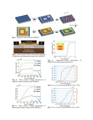
substrate. A 200 nm Sn-doped Ga2O3 epitaxial layer was grown by ozone MBE. The MOSFET fabrication process
flow is shown in Fig. 1. First, a blanket layer of 20 nm SiO2 was deposited on the wafer by plasma enhanced ALD.
Then, silicon dioxide layer in the source/drain (S/D) region was etched away by CF4/O2 based reactive ion etching
(RIE). After a short BCl3/Ar RIE treatment, Ti/Au S/D contact metal was deposited. The contacts were then annealed
under N2 atmosphere to make them ohmic. For the gate, Ti/Au electrodes were defined by standard photolithography
and lift-off procedure for depletion mode MOSFET, while Pt/Au stack was used for enhancement mode devices. The
cross-section schematic of the final MOSFET is shown in Fig .2.
The capacitance-voltage (C-V) characteristics of the MOSCAPs were measured with Agilent 4294A
precision impedance analyzer and the MOSFET IV characteristics were measured with HP 4155B semiconductor
parameter analyzer. Fig. 3 shows a C-V curve for enhancement mode device. The output current-voltage
characteristics of depletion and enhancement mode MOSFET are shown in Fig. 4 and Fig. 6, respectively. Fig. 5 and
Fig. 7 show the corresponding input transfer characteristics. In Fig. 5, from the intercept of linear curve with x-axis,
threshold voltage is ~ -4V for the depletion mode device with Ti/Au gate stack. While, the extracted threshold voltage
from Fig. 7 is 3V for the enhancement mode device with Pt/Au gate stack. The on current for the depletion mode and
enhancement mode devices are 48.7μA (Vgs = 12 V, Vds = 30V) and 45μA (Vgs = 8 V, Vds = 30V) respectively. The
ON/OFF ratio for both devices is ~106
. The drain source breakdown voltage in off state of the devices are 399 V and
390 V respectively for the depletion mode and enhancement mode devices. Both devices show similar breakdown
voltages due to the same gate to drain spacing.
The on state drain current is limited by the high parasitic source/drain resistance. The TLM structures show
a show high resistance with linear behavior. This high source/drain resistance is due to the low doping density in the
epitaxial layer. The extracted active doping density from the C-V curve in Fig. 3 is 6.34×10¹⁵
/cm3
which is lower than
the target doping of ~1017
/cm3
, which increases both the contact resistance and source access region resistance.
Increasing doping density and incorporation of ion-implantation will reduce the source drain parasitic resistance.
In conclusion, we demonstrated a depletion mode MOSFET with SiO2/Ga2O3 structure and also the first
successful enhancement mode MOSFET on β-Ga2O3 with near 400 V drain source breakdown voltage, which is
promising for future Ga2O3 power devices. Advanced devices structure with reduced parasitic source/drain resistance
will enable low ON resistance and higher breakdown voltages.
The authors thank the SUNY MAM program for supporting the work. The work was performed in the Davis Hall cleanroom facility
at the University at Buffalo.
[1] M. Higashiwaki et al, Appl. Phys. Lett., 100, 013504, (2012). [2] E. G. Víllora et al, J. Cryst. Growth, 270, no. 420, (2004).
[3] M. Higashiwaki et al, Appl. Phys. Lett., 103, 123511, (2013). [4] K. Sasaki et al, IEEE Electron Device Lett., 34, 493, (2013).
[5] Y. Jia et al, Appl. Phys. Lett., 106, 102107, 2015](https://image.slidesharecdn.com/2c8e3201-0fde-4c92-b3f4-455fade56d2b-160909220440/85/DRC2016-1-320.jpg)
![Depletion and Enhancement Mode β-Ga2O3 MOSFETs with ALD SiO2 gate
and near 400 V Breakdown Voltage
Ke Zeng1*
, K. Sasaki2
, A. Kuramata2
, T. Masui2
, and Uttam Singisetti1*
1
Electrical Engineering Department, University at Buffalo (SUNY), Buffalo, NY, 14226, USA
2
Novel Crystal Technology, Inc., Sayama, Saitama 350-1328, Japan
*Email: kzeng2@buffalo.edu / Phone: (716) 645-1017
As a next generation wide bandgap semiconductor for power electronics, β-Ga2O3 (Ga2O3) has shown a lot
of potential in recent studies. It has been reported to have high Baliga’s Figure of Merit (BFoM), a figure of merit for
power devices, next only to diamond among wide bandgap semiconductor materials [1]. Moreover, a mature growth
technology for large area substrates is a major practical advantage for cost effectiveness and rapid adaptation by
industry [2]. Because of the advantages of this material, depletion mode MOSFETs and Schottky diodes based on
Ga2O3 with high breakdown voltages have been recently demonstrated [3][4]. However, enhancement mode
MOSFETs are preferred in power electronics applications. All the previous work incorporated ALD Al2O3 as gate
barrier due to its high dielectric constant. However, a recent study reported that SiO2/Ga2O3 interface has a much
bigger conduction band offset than that of Al2O3/Ga2O3 [5] which is preferred in MOSFET. In addition, SiO2/Ga2O3
interface has a relatively low interface states density according to our recent data. These properties make SiO2 an
attractive gate dielectric for Ga2O3 power MOSFETs. Here, we first report depletion mode MOSFET on MBE grown
Ga2O3 with an ALD SiO2 gate. We also report the first successful enhancement mode MOSFET on β-Ga2O3. Both
depletion mode and enhancement mode MOSFETs show near 400 V off state drain source breakdown voltage.
All the devices were fabricated on MBE grown Ga2O3 epitaxial layer on Fe-doped semi-insulating Ga2O3
substrate. A 200 nm Sn-doped Ga2O3 epitaxial layer was grown by ozone MBE. The MOSFET fabrication process
flow is shown in Fig. 1. First, a blanket layer of 20 nm SiO2 was deposited on the wafer by plasma enhanced ALD.
Then, silicon dioxide layer in the source/drain (S/D) region was etched away by CF4/O2 based reactive ion etching
(RIE). After a short BCl3/Ar RIE treatment, Ti/Au S/D contact metal was deposited. The contacts were then annealed
under N2 atmosphere to make them ohmic. For the gate, Ti/Au electrodes were defined by standard photolithography
and lift-off procedure for depletion mode MOSFET, while Pt/Au stack was used for enhancement mode devices. The
cross-section schematic of the final MOSFET is shown in Fig .2.
The capacitance-voltage (C-V) characteristics of the MOSCAPs were measured with Agilent 4294A
precision impedance analyzer and the MOSFET IV characteristics were measured with HP 4155B semiconductor
parameter analyzer. Fig. 3 shows a C-V curve for enhancement mode device. The output current-voltage
characteristics of depletion and enhancement mode MOSFET are shown in Fig. 4 and Fig. 6, respectively. Fig. 5 and
Fig. 7 show the corresponding input transfer characteristics. In Fig. 5, from the intercept of linear curve with x-axis,
threshold voltage is ~ -4V for the depletion mode device with Ti/Au gate stack. While, the extracted threshold voltage
from Fig. 7 is 3V for the enhancement mode device with Pt/Au gate stack. The on current for the depletion mode and
enhancement mode devices are 48.7μA (Vgs = 12 V, Vds = 30V) and 45μA (Vgs = 8 V, Vds = 30V) respectively. The
ON/OFF ratio for both devices is ~106
. The drain source breakdown voltage in off state of the devices are 399 V and
390 V respectively for the depletion mode and enhancement mode devices. Both devices show similar breakdown
voltages due to the same gate to drain spacing.
The on state drain current is limited by the high parasitic source/drain resistance. The TLM structures show
a show high resistance with linear behavior. This high source/drain resistance is due to the low doping density in the
epitaxial layer. The extracted active doping density from the C-V curve in Fig. 3 is 6.34×10¹⁵
/cm3
which is lower than
the target doping of ~1017
/cm3
, which increases both the contact resistance and source access region resistance.
Increasing doping density and incorporation of ion-implantation will reduce the source drain parasitic resistance.
In conclusion, we demonstrated a depletion mode MOSFET with SiO2/Ga2O3 structure and also the first
successful enhancement mode MOSFET on β-Ga2O3 with near 400 V drain source breakdown voltage, which is
promising for future Ga2O3 power devices. Advanced devices structure with reduced parasitic source/drain resistance
will enable low ON resistance and higher breakdown voltages.
The authors thank the SUNY MAM program for supporting the work. The work was performed in the Davis Hall cleanroom facility
at the University at Buffalo.
[1] M. Higashiwaki et al, Appl. Phys. Lett., 100, 013504, (2012). [2] E. G. Víllora et al, J. Cryst. Growth, 270, no. 420, (2004).
[3] M. Higashiwaki et al, Appl. Phys. Lett., 103, 123511, (2013). [4] K. Sasaki et al, IEEE Electron Device Lett., 34, 493, (2013).
[5] Y. Jia et al, Appl. Phys. Lett., 106, 102107, 2015](https://image.slidesharecdn.com/2c8e3201-0fde-4c92-b3f4-455fade56d2b-160909220440/75/DRC2016-1-2048.jpg)


![workjnuuuuuuuuuuuooooooooooooooooooouuuuuuuuuuuuuuuuuuuuuuuuuu]]](https://cdn.slidesharecdn.com/ss_thumbnails/baippdtcblop01fie-251222045342-5aabffab-thumbnail.jpg?width=640&height=640&fit=bounds)


