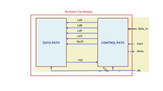
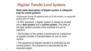
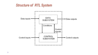
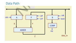
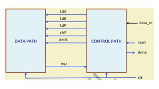
The document describes the register transfer level (RTL) approach to modeling digital systems. It discusses how RTL systems are divided into a data system and control system. The data system consists of registers to store state, and the function is performed through a sequence of register transfers controlled by the control system. An example of multiplying two numbers using repeated addition is provided. The data path and control path for this example are shown using Verilog code. Modules like registers, adders, comparators are defined to implement the data path, and a finite state machine controls the data transfers.

![Verilog Code for Data Path
module MUL_datapath (eqz, LdA, LdB, LdP, clrP, decB, data_in, clk);
input LdA, LdB, LdP, clrP, decB, clk;
input [15:0] data_in;
output eqz;
wire [15:0] X, Y, Z, Bout;
PIPO1 A (X, data_in, LdA, clk);
PIPO2 P (Y, Z, LdP, clrP, clk);
CNTR B (Bout, data_in, LdB, decB, clk);
ADD ADDER (Z, X, Y);
EQZ COMP (eqz, Bout);
endmodule
Bout](https://image.slidesharecdn.com/datapathcontrolpathpruned-240331104126-dedde151/85/Datapath_control_path_pruned-pptxhghygvvgygh-8-320.jpg)
![Verilog Code for Data Path modules
module PIPO1 (dout, din, ld, clk);
input [15:0] din;
input ld, clk; output reg [15:0] dout;
always @(posedge clk)
if (ld) dout <= din;
endmodule
module PIPO2 (dout, din, ld, clr, clk);
input [15:0] din;
input ld, clr, clk;
output reg [15:0] dout;
always @(posedge clk)
if (clr) dout <= 16’b0;
else if (ld) dout <= din;
endmodule
PIPO1 A (X, data_in, LdA, clk);
PIPO2 P (Y, Z, LdP, clrP, clk);](https://image.slidesharecdn.com/datapathcontrolpathpruned-240331104126-dedde151/85/Datapath_control_path_pruned-pptxhghygvvgygh-9-320.jpg)
![module ADD (out, in1, in2);
input [15:0] in1, in2;
output reg [15:0] out;
always @(*)
out = in1 + in2;
endmodule
Verilog Code for Data Path modules
module EQZ (eqz, data);
input [15:0] data;
output eqz;
assign eqz = (data == 0);
endmodule
module CNTR (dout, din, ld, dec, clk);
input [15:0] din;
input ld, dec, clk;
output reg [15:0] dout;
always @(posedge clk)
if (ld) dout <= din;
else if (dec) dout <= dout - 1;
endmodule
CNTR B (Bout, Bus, LdB, decB, clk);
ADD AD (Z, X, Y);
EQZ COMP (eqz, Bout);](https://image.slidesharecdn.com/datapathcontrolpathpruned-240331104126-dedde151/85/Datapath_control_path_pruned-pptxhghygvvgygh-10-320.jpg)
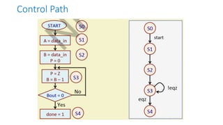
![Verilog Code for Control Path
module controller (LdA, LdB, LdP, clrP, decB, done, clk, eqz, start);
input clk, eqz, start;
output reg LdA, LdB, LdP, clrP, decB, done;
reg [2:0] state, next_state;
parameter S0=3'b000, S1=3'b001, S2=3'b010, S3=3'b011, S4=3'b100;
always @(posedge clk)
if(!start)
begin state <= S0; LdA = 0; LdB = 0; LdP = 0; clrP = 0; decB = 0; done=0; end
else state <= next_state;
always @(state or eqz or start)
begin
case (state)
S0: if (start) next_state <= S1; else next_state <= S0;
S1: begin next_state <= S2; LdA=1; end
S2: begin next_state <= S3; LdA = 0; LdB = 1; clrP = 1; end
S3: begin if (eqz) next_state <= S4; else next_state <= S3;
LdB = 0; LdP = 1; clrP = 0; decB = 1; end
S4: begin next_state <= S0; done = 1; LdB = 0; LdP = 0; decB = 0; end
default: next_state <= S0;
endcase end endmodule
FSM/Controller
start
eqz
outputs](https://image.slidesharecdn.com/datapathcontrolpathpruned-240331104126-dedde151/85/Datapath_control_path_pruned-pptxhghygvvgygh-11-320.jpg)