SlideShare a Scribd company logo
Introduction to Amplifiers
In "Electronics", signal amplifiers are widely used devices as they have the ability to amplify a
relatively small input voltage signal, for example from a Sensor or microphone, into a much
larger output signal to drive a Relay, lamp or loudspeaker for example. There are many forms of
amplifiers, from Operational Amplifiers and Small Signal Amplifiers up to Large Signal and
Power Amplifiers. Amplifiers can be thought of as a simple box or block containing the
amplifying device, such as a Transistor, Field Effect Transistor or Op-amp
An amplifier has three main properties, Input Resistance or (Rin), Output Resistance or (Rout)
and of course Gain or (A). No matter how complicated an amplifier circuit is, a general amplifier
model can be used to show the relationship of these three properties.
, and which has two
input terminals and two output terminals with the output signal being greater than that of the
input signal, being "Amplified".
Ideal Amplifier Model
The difference between the input and output signals is known as the Gain of the amplifier and is
basically a measure of how much an amplifier "amplifies" the input signal. For example, if we
have an input signal of 1 and an output of 50, then the gain of the amplifier would be 50. Gain is
a ratio, it has no units but is given the symbol "A", which can be simply calculated as the output
signal divided by the input signal.
Amplifier Gain
Then the gain of an amplifier can be said to be the relationship that exists between the signal
measured at the output with the signal measured at the input. There are three different kinds of
Amplifier Gain, Voltage Gain (Av), Current Gain (Ai) and Power Gain (Ap) and examples of
these are given below.
www.getmyuni.com
Amplifier Gain of the Input Signal
Voltage Amplifier Gain
Current Amplifier Gain
Power Amplifier Gain
Note that for the Power Gain you can also divide the power obtained at the output with the power
obtained at the input. Also, the subscripts v, i and p denote the type of signal gain.
The power Gain of the amplifier can also be expressed in Decibels, (dB). The Bel is a
logarithmic unit (base 10) of measurement that has no units but as the Bel is a large unit of
measure, it has be prefixed with deci making it Decibels with one decibel being one tenth
(1/10th) of a Bel. To calculate the gain of the amplifier in Decibels or dB, we can use the
following expressions.
• Voltage Gain in dB: av = 20 log Av
•
• Current Gain in dB: ai = 20 log Ai
•
• Power Gain in dB: ap = 10 log Ap
Note that the DC power gain of an amplifier is equal to ten times the common log of the output
to input ratio, where as voltage and current gains are 20 times the common log of the ratio. Also,
a positive value of dB represents a Gain and a negative value of dB represents a Loss within the
www.getmyuni.com
amplifier. For example, an amplifier gain of +3dB indicates that the output signal has "doubled",
(x2) while an amplifier gain of -3dB indicates that the signal has "halved", (x0.5) or in other
words a loss.
Example No1
Determine the Voltage, Current and Power Gain of an amplifier that has an input signal of 1mA
at 10mV and a corresponding output signal of 10mA at 1V. Also, express all three gains in
decibels, (dB).
Amplifier Gain.
in Decibels (dB).
Then the amplifier has a Voltage Gain of 100, a Current Gain of 10 and a Power Gain of 1,000.
Amplifiers can be divide into two distinct types, Small Signal Amplifiers such as pre-
amplifiers, instrumentation amplifiers etc, which are designed to amplify very small signal
voltage levels of only a few micro-volts (μV) from sensors or audio signals and Large Signal
Amplifiers such as audio power amplifiers or switching amplifiers, which are designed to
amplify large input voltage signals or switch high current loads.
Power Amplifiers
Small signal amplifiers are generally referred to as "Voltage" amplifiers as they convert a small
input voltage into a much larger output voltage. Sometimes an amplifier is required to drive a
www.getmyuni.com
motor or feed a loudspeaker and for these types of applications where high switching currents are
needed Power Amplifiers are required.
The main function of Power amplifiers (also known as large signal amplifiers) is to deliver
power, which as we know from above, is the product of the voltage and current applied to the
load. The power amplifier works on the basic principle of converting the DC power drawn from
the power supply into an AC voltage signal delivered to the load. Although the amplification is
high the efficiency of the conversion from the DC power supply input to the AC voltage signal
output is usually poor. The perfect or ideal amplifier would give us an efficiency rating of 100%
or at least the power IN is equal to the power OUT. However, this can never happen as some of
its power is lost in the form of heat and also, the amplifier itself consumes power during the
amplification process. Then the efficiency of an amplifier is given as:
Amplifier Efficiency
Amplifier Classes
We saw in the Common Emitter
Audio Power Amplifiers are classified in order according to their circuit configurations and
mode of operation being designated different classes of operation in alphabetical order such as
A, B, C, AB, etc. These different classes of operation range from a near linear output but with
low efficiency to a non-linear output but with a high efficiency. There are typical maximum
efficiencies for the various types or class of amplifier, with the most commonly used being:
transistor tutorial that for the transistor to operate within its
"Active Region" some form of "Base Biasing" was required. This small Base Bias voltage added
to the input signal allowed the transistor to reproduce the full input waveform at its output with
no loss of signal. However, by altering the position of this Base Bias voltage, it is possible to
operate an amplifier in an amplification mode other than that for full waveform reproduction. By
changing the amplifiers Base bias voltage different ranges or modes of operation can be obtained
and these are categorized according to their Class.
• Class A - a maximum theoretical efficiency of less than 40%
•
• Class B - with a maximum theoretical efficiency of about 70%
•
• Class AB - which an efficiency rating between that of Class A and Class B
Class A Operation
Class A Amplifier operation is were the entire input signal waveform is faithfully reproduced at
the amplifiers output as the transistor is perfectly biased within its active region, thereby never
www.getmyuni.com
reaching either of its Cut-off or Saturation regions. This then results in the AC input signal being
perfectly "centered" between the amplifiers upper and lower signal limits as shown below.
Class A Output Waveform
Here, the Class A amplifier uses the same transistor for both halves of the output waveform and
due to its biasing arrangement always has current flowing through it, even if there is no input
signal. In other words the output transistors never turns "OFF". This results in the class A type of
operation being very inefficient as its conversion of the DC supply power to the AC signal power
delivered to the load is usually very low. Generally, the output transistor of a Class A amplifier
gets very hot even when there is no input signal present so some form of heatsinking is required.
The DC current flowing through the output transistor (Ic) when there is no output signal will be
equal to the current flowing through the load.
Class B Operation
Unlike the Class A amplifier above that uses a single transistor for its output stage, the Class B
Amplifier uses two complimentary transistors (an NPN and a PNP) for each half of the output
waveform. One transistors for the positive half of the waveform and another for the negative half
of the waveform. This means that each transistor spends half of its time in the Active region and
half its time in the Cut-off region. Class B operation has no DC bias voltage instead the transistor
only conducts when the input signal is greater than the base-emitter voltage and for silicon
devices is about 0.7v. Therefore, at zero input there is zero output. This then results in only half
the input signal being presented at the amplifiers output giving a greater efficiency as shown
below.
Class B Output Waveform
www.getmyuni.com
As the output transistors for each half of the waveform, both positive and negative, requires a
base-emitter voltage greater than the 0.7v required for the bipolar transistor to start conducting,
the lower part of the output waveform which is below this 0.7v window will not be reproduced
accurately resulting in a distorted area of the output waveform as one transistor turns "OFF"
waiting for the other to turn back "ON". This type of distortion is called Crossover Distortion
and is looked at later on in this section.
Class AB Operation
The Class AB Amplifier is a compromise between the Class A and the Class B configurations
above. While Class AB operation still uses two complementary transistors in its output stage a
very small biasing voltage is applied to the Base of the transistor to bias it close to the Cut-off
region when no input signal is present. An input signal will cause the transistor to operate as
normal in its Active region thereby eliminating any crossover distortion. A small Collector
current will flow when there is no input signal but it is much less than that for the Class A
amplifier configuration. This means then that the transistor will be "ON" for more than half a
cycle of the waveform. This type of amplifier configuration improves both the efficiency and
linearity of the amplifier circuit compared to Class A.
Class AB Output Waveform
www.getmyuni.com
The class of operation for an amplifier is very important as it determines both the efficiency and
the amount of power that the amplifier consumes and dissipates in the form of wasted heat,
which may also require larger power transistors, more expensive heatsinks, cooling fans, or even
an increase in the size of the power supply required to deliver the extra power required by the
amplifier. Power converted into heat from transistors, resistors or any other component makes
any electronic circuit inefficient and will result in premature failure of the device. So why use a
Class A amplifier if its efficiency is less than 40% compared to a Class B amplifier that has a
higher efficiency rating of nearly 70%. Basically, a Class A amplifier gives a more linear output
meaning that it has, Linearity over a larger frequency response.
The Common Emitter Amplifier
In the Transistor tutorial
We also saw that a static or DC load line can be drawn onto these output characteristics curves to
show all the possible operating points of the transistor from fully "ON" to fully "OFF", and to
which the quiescent operating point or Q-point of the amplifier can be found. The aim of any
small signal amplifier is to amplify all of the input signal with the minimum amount of distortion
possible to the output signal, in other words, the output signal must be an exact reproduction of
the input signal but only bigger (amplified). To obtain low distortion when used as an amplifier
we saw that the most common circuit configuration for a transistor is
that of the Common Emitter Amplifier and that a family of curves known commonly as the
Output Characteristics Curves, relates the Collector current (Ic), to the output or Collector
voltage (Vce), for different values of Base current (Ib) signal. All types of signal amplifiers
operate using AC signal inputs which alternate between a positive value and a negative value so
some way of presetting the amplifier circuit to operate between these two maximum or peak
values is required. This is achieved using a process known as Biasing. Biasing is very important
in amplifier design as it establishes the correct operating point of the amplifier ready to receive
signals, thereby reducing any distortion to the input signal.
www.getmyuni.com
the operating quiescent point needs to be correctly selected. This is in fact the DC operating
point of the amplifier and its position may be established at any point along the load line by a
suitable biasing arrangement. The best possible position for this Q-point is as close to the centre
position of the load line as reasonably possible, thereby producing a Class A type amplifier
operation, ie. Vce = 1/2Vcc. Consider the Common Emitter Amplifier circuit shown below.
The Common Emitter Amplifier Circuit
The amplifier circuit shown above uses what is commonly called "Voltage Divider Biasing".
This type of biasing arrangement is commonly used in the design of bipolar transistor amplifier
circuits and which greatly reduces the effects of varying Beta, (β) by holding the Base bias at a
constant steady voltage allowing for best stability. The quiescent Base voltage (Vb) is
determined by the potential divider network formed by the two resistors, R1 and R2 and the
power supply voltage Vcc. The voltage level generated at the junction of resistors R1 and R2
holds the Base voltage (Vb) constant at a value below the supply voltage. This reference voltage
can be easily calculated using the simple voltage divider formula:
This same supply voltage, (Vcc) also determines the maximum Collector current, Ic when the
transistor is switched fully "ON" (saturation), Vce = 0. The Base current Ib for the transistor is
found from the Collector current, Ic and the DC current gain Beta, β of the transistor.
www.getmyuni.com
Beta is sometimes referred to as hFE which is the transistors forward current gain in the common
emitter configuration. Beta has no units as it is a fixed ratio of the two currents, Ic and Ib so a
small change in the Base current will cause a large change in the Collector current. One final
point about Beta. Transistors of the same type and part number will have large variations in their
Beta value for example, the BC107 NPN Bipolar transistor has a DC current gain Beta value of
between 110 and 450 (data sheet value) this is because Beta is a characteristic of their
construction.
As the Base/Emitter junction is forward-biased, the Emitter voltage, Ve will be one junction
voltage drop different to the Base voltage. If the voltage across the Emitter resistor is known then
the Emitter current, Ie can be easily calculated using Ohm's Law
Example No1
. The Collector current, Ic can be
approximated, since it is almost the same value as the Emitter current.
Assuming a load resistor, RL of 1.2kΩs and a supply voltage of 12v. Calculate the maximum
Collector current (Ic) flowing through the load resistor when the transistor is switched fully
"ON", assume Vce = 0. Also find the value of the Emitter resistor, RE with a voltage drop of 1v
across it and the values of all the other resistors assuming a silicon transistor.
This then establishes point "A" on the Collector current vertical axis of the characteristics curves
and occurs when Vce = 0. When the transistor is switched fully "OFF", their is no voltage drop
across either resistor RE or RL as no current is flowing through them. Then the voltage drop
across the transistor, Vce is equal to the supply voltage, Vcc. This then establishes point "B" on
the horizontal axis of the characteristics curves. Generally, the quiescent Q-point of the amplifier
is with zero input signal applied to the Base, so the Collector sits half-way along the load line
between zero volts and the supply voltage, (Vcc/2). Therefore, the Collector current at the Q-
point of the amplifier will be given as:
This static DC load line produces a straight line equation whose slope is given as: -1/(RL + RE)
and that it crosses the vertical Ic axis at a point equal to Vcc/(RL + RE). The actual position of the
Q-point on the DC load line is determined by the mean value of Ib.
www.getmyuni.com
As the Collector current, Ic of the transistor is also equal to the DC gain of the transistor (Beta),
times the Base current (β x Ib), if we assume a Beta (β) value for the transistor of say 100, (one
hundred is a reasonable average value for low power signal transistors) the Base current Ib
flowing into the transistor will be given as:
Instead of using a separate Base bias supply, it is usual to provide the Base Bias Voltage from
the main supply rail (Vcc) through a dropping resistor, R1. Resistors, R1 and R2 can now be
chosen to give a suitable quiescent Base current of 45.8μA or 46μA rounded off. The current
flowing through the potential divider circuit has to be large compared to the actual Base current,
Ib, so that the voltage divider network is not loaded by the Base current flow. A general rule of
thumb is a value of at least 10 times Ib flowing through the resistor R2. Transistor Base/Emitter
voltage, Vbe is fixed at 0.7V (silicon transistor) then this gives the value of R2 as:
If the current flowing through resistor R2 is 10 times the value of the Base current, then the
current flowing through resistor R1 in the divider network must be 11 times the value of the Base
current. The voltage across resistor R1 is equal to Vcc - 1.7v (VRE + 0.7 for silicon transistor)
which is equal to 10.3V, therefore R1 can be calculated as:
The value of the Emitter resistor, RE can be easily calculated using Ohm's Law. The current
flowing through RE is a combination of the Base current, Ib and the Collector current Ic and is
given as:
Resistor, RE is connected between the Emitter and ground and we said previously that it has a
voltage of 1 volt across it. Then the value of RE is given as:
www.getmyuni.com
So, for our example above, the preferred values of the resistors chosen to give a tolerance of 5%
(E24) are:
Then, our original Common Emitter circuit above can be rewritten to include the values of the
components that we have just calculated.
Completed Common Emitter Circuit
Coupling Capacitors
In common emitter amplifier circuits, capacitors C1 and C2 are used as Coupling Capacitors to
separate the AC signals from the DC bias. This ensures that the bias condition set up for the
circuit to operate correctly is not effected by any additional amplifier stages, as the capacitors
will only pass AC signals and block any DC component. The output AC signal is then
superimposed on the biasing of the following stages. Also a bypass capacitor, CE is included in
the Emitter leg circuit. This capacitor is an open circuit component for DC bias meaning that the
biasing currents and voltages are not affected by the addition of the capacitor maintaining a good
Q-point stability. However, this bypass capacitor short circuits the Emitter resistor at high
frequency signals and only RL plus a very small internal resistance acts as the transistors load
increasing the voltage gain to its maximum. Generally, the value of the bypass capacitor, CE is
www.getmyuni.com
chosen to provide a reactance of at most, 1/10th the value of RE at the lowest operating signal
frequency.
Output Characteristics Curves
Ok, so far so good. We can now construct a series of curves that show the Collector current, Ic
against the Collector/Emitter voltage, Vce with different values of Base current, Ib for our simple
common emitter amplifier circuit. These curves are known as the "Output Characteristic Curves"
and are used to show how the transistor will operate over its dynamic range. A static or DC load
line is drawn onto the curves for the load resistor RL of 1.2kΩ to show all the transistors possible
operating points. When the transistor is switched "OFF", Vce equals the supply voltage Vcc and
this is point B on the line. Likewise when the transistor is fully "ON" and saturated the Collector
current is determined by the load resistor, RL and this is point A on the line. We calculated
before from the DC gain of the transistor that the Base current required for the mean position of
the transistor was 45.8μA and this is marked as point Q on the load line which represents the
Quiescent point or Q-point of the amplifier. We could quite easily make life easy for ourselves
and round off this value to 50μA exactly, without any effect to the operating point.
Output Characteristics Curves
www.getmyuni.com
Point Q on the load line gives us the Base current Q-point of Ib = 45.8μA or 46μA. We need to
find the maximum and minimum peak swings of Base current that will result in a proportional
change to the Collector current, Ic without any distortion to the output signal. As the load line
cuts through the different Base current values on the DC characteristics curves we can find the
peak swings of Base current that are equally spaced along the load line. These values are marked
as points N and M on the line, giving a minimum and a maximum Base current of 20μA and
80μA respectively. These points, N and M can be anywhere along the load line that we choose as
long as they are equally spaced from Q. This then gives us a theoretical maximum input signal to
the Base terminal of 30μA peak-to-peak without producing any distortion to the output signal.
Any input signal giving a Base current greater than this value will drive the transistor to go
beyond point N and into its Cut-off region or beyond point M and into its Saturation region
thereby resulting in distortion to the output signal in the form of "clipping".
Using points N and M as an example, the instantaneous values of Collector current and
corresponding values of Collector-emitter voltage can be projected from the load line. It can be
www.getmyuni.com
seen that the Collector-emitter voltage is in anti-phase (-180o
) with the collector current. As the
Base current Ib changes in a positive direction from 50μA to 80μA, the Collector-emitter
voltage, which is also the output voltage decreases from its steady state value of 5.8v to 2.0v.
Then a single stage Common Emitter Amplifier is also an "Inverting Amplifier" as an increase
in Base voltage causes a decrease in Vout and a decrease in Base voltage produces an increase in
Vout.
Voltage Gain
The Voltage Gain of the common emitter amplifier is equal to the ratio of the change in the
input voltage to the change in the amplifiers output voltage. Then ΔVL is Vout and ΔVB is Vin.
But voltage gain is also equal to the ratio of the signal resistance in the Collector to the signal
resistance in the Emitter and is given as:
We mentioned earlier that as the signal frequency increases the bypass capacitor, CE starts to
short out the Emitter resistor. Then at high frequencies RE = 0, making the
gain infinite. However, bipolar transistors have a small internal resistance
built into their Emitter region called Re. The transistors semiconductor
material offers an internal resistance to the flow of current through it and is
generally represented by a small resistor symbol shown inside the main
transistor symbol. Transistor data sheets tell us that for a small signal bipolar
transistors this internal resistance is the product of 25mV ÷ Ie (25mV being
the internal volt drop across the Base/Emitter junction depletion layer), then for our common
Emitter amplifier circuit above this resistance value will be equal to:
This internal Emitter leg resistance will be in series with the external Emitter resistor, RE, then
the equation for the transistors actual gain will be modified to include this internal resistance and
is given as:
At low frequency signals the total resistance in the Emitter leg is equal to RE + Re. At high
frequency, the bypass capacitor shorts out the Emitter resistor leaving only the internal resistance
Re in the Emitter leg resulting in a high gain. Then for our common emitter amplifier circuit
above, the gain of the circuit at both low and high signal frequencies is given as:
www.getmyuni.com
At Low Frequencies
At High Frequencies
One final point, the voltage gain is dependent only on the values of the Collector resistor, RL and
the Emitter resistance, (RE + Re) it is not affected by the current gain Beta, β (hFE) of the
transistor.
So, for our simple example above we can now summarise all the values we have calculated for
our common emitter amplifier circuit and these are:
Minimum Mean Maximum
Base Current 20μA 50μA 80μA
Collector Current 2.0mA 4.8mA 7.7mA
Output Voltage Swing 2.0V 5.8V 9.3V
Amplifier Gain -5.32 -218
Summary
Then to summarize, The Common Emitter Amplifier circuit has a resistor in its Collector
circuit. The current flowing through this resistor produces the voltage output of the amplifier.
The value of this resistor is chosen so that at the amplifiers quiescent operating point, Q-point
this output voltage lies half way along the transistors load line.
The Base of the transistor used in a common Emitter amplifier is biased using two resistors as a
potential divider network. This type of biasing arrangement is commonly used in the design of
bipolar transistor amplifier circuits and greatly reduces the effects of varying Beta, (β) by
holding the Base bias at a constant steady voltage. This type of biasing produces the greatest
stability.
A resistor can be included in the Emitter leg in which case the voltage gain becomes -RL/RE. If
there is no external Emitter resistance, the voltage gain of the amplifier is not infinite as there is a
very small internal resistance, Re in the Emitter leg. The value of this internal resistance is equal
to 25mV/IE
www.getmyuni.com
RESET
JFET Amplifier
So far we have looked at the Bipolar type amplifiers and especially the Common Emitter
amplifier, but small signal amplifiers can also be made using Field Effect Transistors or FET's.
These devices have the advantage over bipolar devices of having an extremely high input
impedance along with a low noise output making them very useful in amplifier circuits using
very small signals. The design of an amplifier circuit based around a JFET (n-channel FET for
this example) or even a MOSFET is exactly the same principle as that for a bipolar device and
for a Class A amplifier as we looked at in the previous tutorial. A suitable Quiescent point still
needs to be found for the correct biasing of the amplifier circuit with amplifier configurations of
Common Source, Common Drain and Common Gate available for FET devices. In this tutorial
we will look at the JFET Amplifier as a common source amplifier as this is the most widely
used design. Consider the Common Source JFET Amplifier circuit below.
Common Source JFET Amplifier
The circuit consists of an N-channel JFET, but the device could also be an equivalent N-channel
Depletion-mode MOSFET as the circuit diagram would be the same, just a change in the FET.
The JFET Gate voltage Vg is biased through the potential divider network set up by resistors R1
and R2 and is biased to operate within its saturation region which is equivalent to the active
region of the BJT. The Gate biasing voltage Vg is given as:
www.getmyuni.com
Note that this equation only determines the ratio of the resistors R1 and R2, but in order to take
advantage of the very high input impedance of the JFET as well as reducing the power
dissipation within the circuit, we need to make these resistor values as high as possible, with
values in the order of 1 to 10MΩ being common.
The input signal, (Vin) is applied between the Gate terminal and 0v with the Drain circuit
containing the load resistor, Rd. The output voltage, Vout is developed across this load
resistance. There is also an additional resistor, Rs included in the Source lead and the same Drain
current also flows through this resistor. When the JFET is switched fully "ON" a voltage drop
equal to Rs x Id is developed across this resistor raising the potential of the Source terminal
above 0v or ground level. This voltage drop across Rs due to the Drain current provides the
necessary reverse biasing condition across the Gate resistor, R2. In order to keep the Gate-source
junction reverse biased, the Source voltage, Vs needs to be higher than the gate voltage, Vg. This
Source voltage is therefore given as:
Then the Drain current, Id is also equal to the Source current, Is as "No Current" enters the Gate
terminal and this can be given as:
This potential divider biasing circuit improves the stability of the common source JFET circuit
when being fed from a single DC supply compared to that of a fixed voltage biasing circuit. Both
Resistor, Rs and Capacitor, Cs serve basically the same function as the Emitter resistor and
capacitor in the Common Emitter Bipolar Transistor amplifier circuit, namely to provide good
stability and prevent a reduction in the signal gain. However, the price paid for a stabilized
quiescent Gate voltage is that more of the supply voltage is dropped across Rs.
The basic circuit and characteristics of a common source JFET amplifier are very similar to that
of the Common Emitter amplifier. A DC load line is constructed by joining the two points
relating to the Drain current, Id and the supply voltage, Vdd intersecting the curves at the Q-
point as follows.
JFET Amplifier Characteristics Curves
www.getmyuni.com
As with the Common Emitter circuit, the DC load line produces a straight line equation whose
gradient is given as: -1/(Rd + Rs) and that it crosses the vertical Id axis at a point equal to
Vdd/(Rd + Rs). The other end of the load line crosses the horizontal axis at a point equal to Vdd.
The actual position of the Q-point on the DC load line is determined by the mean value of Vg
which is biased negatively as the JFET as a depletion-mode device. Like the bipolar common
emitter amplifier the output of the Common Source JFET Amplifier is 1800
out of phase with
the input signal.
One of the main disadvantages of using Depletion-mode JFET is that they need to be negatively
biased. Should this bias fail for any reason the Gate-source voltage may rise and become positive
causing an increase in Drain current resulting in failure of the Drain voltage, Vd. Also the high
channel resistance, Rds(on) of the JFET, coupled with high quiescent steady state Drain current
makes these devices run hot so additional heatsink is required. However, most of the problems
associated with using JFET's can be greatly reduced by using enhancement-mode MOSFET
devices instead.
www.getmyuni.com
MOSFETs
Amplifier Distortion
or Metal Oxide Semiconductor FET's have much higher input impedances and low
channel resistances compared to the equivalent JFET. Also the biasing arrangements for
MOSFETs are different and unless we bias them positively for N-channel devices and negatively
for P-channel devices no Drain current will flow, then we have in effect a fail safe transistor.
From the previous tutorials we learnt that for a signal amplifier to work correctly it requires some
form of DC Bias on its Base or Gate terminal so that it amplifies the input signal over its entire
cycle with the bias Q-point set as near to the middle of the load line as possible. This then gave
us a Class "A" type amplification with the most common configuration being Common Emitter
for Bipolar transistors and Common Source for unipolar transistors. We also saw that the Power,
Voltage or Current Gain, (amplification) provided by the amplifier is the ratio of the peak input
value to its peak output value. However, if we incorrectly design our amplifier circuit and set the
biasing Q-point at the wrong position on the load line or apply too large an input signal, the
resultant output signal may not be an exact reproduction of the original input signal waveform.
Consider the common emitter amplifier circuit below.
Common Emitter Amplifier
Distortion of the signal waveform may take place because:
• 1. Amplification may not be taking place over the whole signal cycle due to incorrect
biasing.
•
• 2. The input may be too large, causing the amplifier to limit.
•
• 3. The amplification may not be linear over the entire frequency range of inputs.
www.getmyuni.com
This means then that during the amplification process of the signal waveform, some form of
Amplifier Distortion has occurred.
Amplitude Distortion
Amplifiers are basically designed to amplify small voltage input signals into much larger output
signals and this means that the output signal is constantly changing by some factor or value times
the input signal at all input frequencies. We saw previously that this multiplication factor is
called the Beta, β value of the transistor. Common Emitter or even common Source type circuits
work fine for small AC input signals but suffer from one major disadvantage, the bias Q-point of
a bipolar amplifier depends on the same Beta value which may vary from transistors of the same
type, ie. the Q-point for one transistor is not necessarily the same as the Q-point for another
transistor of the same type due to the inherent manufacturing tolerances. If this occurs the
amplifier may not be linear and Amplitude Distortion will result but careful choice of the
transistor can minimise this effect.
Amplitude distortion occurs when the peak values of the frequency waveform are attenuated
causing distortion due to a shift in the Q-point and amplification may not take place over the
whole signal cycle. This non-linearity of the output waveform is shown below.
Amplitude Distortion due to Incorrect Biasing
If the bias is correct the output waveform should look like that of the input waveform only
bigger, (amplified). If there is insufficient bias the output waveform will look like the one on the
right with the negative part of the output waveform "cut-off". If there is too much bias the output
waveform will look like the one on the left with the positive part "cut-off". When the bias
voltage is too small, during the negative part of the cycle the transistor does not conduct fully so
the output is set by the supply voltage. When the bias is too great the positive part of the cycle
saturates the transistor and the output drops almost to zero.
www.getmyuni.com
Even with the correct biasing voltage level set, it is still possible for the output waveform to
become distorted due to a large input signal being amplified by the circuits gain. The output
voltage signal becomes clipped in both the positive and negative parts of the waveform an no
longer resembles a sine wave, even when the bias is correct. This type of amplitude distortion is
called Clipping and is the result of "Over-driving" the input of the amplifier.
When the input amplitude becomes too large, the clipping becomes substantial and forces the
output waveform signal to exceed the power supply voltage rails with the peak (+ve half) and the
trough (-ve half) parts of the waveform signal becoming flattened or "Clipped-off". To avoid this
the maximum value of the input signal must be limited to a level that will prevent this clipping
effect as shown above.
Amplitude Distortion due to Clipping
Amplitude Distortion greatly reduces the efficiency of an amplifier circuit. These "flat tops" of
the distorted output waveform either due to incorrect biasing or over driving the input do not
contribute anything to the strength of the output signal at the desired frequency. Having said all
that, some well known guitarist and rock bands actually prefer that their distinctive sound is
highly distorted or "overdriven" by heavily clipping the output waveform to both the +ve and -ve
power supply rails. Also, excessive amounts of clipping can also produce an output which
resembles a "square wave" shape which can then be used in electronic or digital circuits.
We have seen that with a DC signal the level of gain of the amplifier can vary with signal
amplitude, but as well as Amplitude Distortion, other types of distortion can occur with AC
signals in amplifier circuits, such as Frequency Distortion and Phase Distortion.
Frequency Distortion
Frequency Distortion occurs in a transistor amplifier when the level of amplification varies
with frequency. Many of the input signals that a practical amplifier will amplify consist of the
required signal waveform called the "Fundamental Frequency" plus a number of different
www.getmyuni.com
frequencies called "Harmonics" superimposed onto it. Normally, the amplitude of these
harmonics are a fraction of the fundamental amplitude and therefore have very little or no effect
on the output waveform. However, the output waveform can become distorted if these harmonic
frequencies increase in amplitude with regards to the fundamental frequency. For example,
consider the waveform below:
Frequency Distortion due to Harmonics
In the example above, the input waveform consists a the fundamental frequency plus a second
harmonic signal. The resultant output waveform is shown on the right hand side. The frequency
distortion occurs when the fundamental frequency combines with the second harmonic to distort
the output signal. Harmonics are therefore multiples of the fundamental frequency and in our
simple example a second harmonic was used. Therefore, the frequency of the harmonic is 2
times the fundamental, 2 x f or 2f. Then a third harmonic would be 3f, a fourth, 4f, and so on.
Frequency distortion due to harmonics is always a possibility in amplifier circuits containing
reactive elements such as capacitance or inductance.
Phase Distortion
Phase Distortion or Delay Distortion occurs in a non-linear transistor amplifier when there is a
time delay between the input signal and its appearance at the output. If we call the phase change
between the input and the output zero at the fundamental frequency, the resultant phase angle
delay will be the difference between the harmonic and the fundamental. This time delay will
depend on the construction of the amplifier and will increase progressively with frequency
within the bandwidth of the amplifier. For example, consider the waveform below:
Phase Distortion due to Delay
www.getmyuni.com
Any practical amplifier will have a combination of both "Frequency" and "Phase" distortion
together with amplitude distortion but in most applications such as in audio amplifiers or power
amplifiers, unless the distortion is excessive or severe it will not generally affect the operation of
the system.
Class A Amplifier
Common emitter voltage amplifiers are the most commonly used type of amplifier as they have a
large voltage gain. They are designed to produce a large output voltage swing from a relatively
small input signal voltage of only a few millivolt's and are used mainly as "Small Signal
Amplifiers" as we saw in the previous tutorials. However, sometimes an amplifier is required to
drive large resistive loads such as a loudspeaker and for these types of applications where high
switching currents are needed Power Amplifiers are required.
The main function of the Power amplifier, which are also known as a "Large Signal Amplifier" is
to deliver power, which is the product of voltage and current to the load. Basically a power
amplifier is also a voltage amplifier the difference being that the load resistance connected to the
output is relatively low, for example a loudspeaker of 4 or 8Ωs resulting in high currents flowing
through the Collector of the transistor. Because of these high load currents the output
transistor(s) used for power amplifier output stages need to have higher voltage and power
ratings than the general ones used for small signal stages.
Since we are interested in delivering maximum AC power to the load, while consuming the
minimum DC power possible from the supply we are mostly concerned with the "Conversion
Efficiency" of the amplifier. However, one of the main disadvantage of power amplifiers and
especially Class A type amplifiers is that their overall conversion efficiency is very low.
Percentage efficiency in amplifiers is defined as the r.m.s. output power dissipated in the load
divided by the total DC power taken from the supply source as shown below.
Power Amplifier Efficiency
www.getmyuni.com
• Where:
•
• η% - is the efficiency of the amplifier.
•
• Pout - is the amplifiers output power delivered to the load.
•
• Pdc - is the DC power taken from the supply.
For a power amplifier it is very important that the amplifiers power supply is well designed to
provide the maximum available continuous power to the output signal.
Class A Amplifier
The most commonly used type of power amplifier configuration is the Class A Amplifier. Class
A amplifier stages use the transistor in the standard Common Emitter circuit configuration as
seen previously, in which the transistor is always biased "ON" so that it conducts during one
complete cycle of the input signal waveform producing minimum distortion to the output. This
means then that the Class A Amplifier configuration is the ideal operating mode, because there
can be no crossover or switch-off distortion to the output waveform. Class A power amplifier
output stages may use a single transistor or pairs of transistors connected together to share the
high load current. Consider the Class A amplifier circuit below.
Single-ended Amplifier Circuit
www.getmyuni.com
This is the simplest type of Class A power amplifier circuit. It uses a single-ended transistor for
its output stage with the resistive load connected directly to the Collector terminal. When the
transistor switches "ON" it sinks the output current through the Collector resulting in an
inevitable voltage drop across the Emitter resistance thereby limiting the negative output
capability. The efficiency of this type of circuit is very low (possibly 20%) and delivers small
power outputs for a large drain on the DC power supply. A Class A amplifier stage passes the
same load current even when no input signal is applied so large heatsinks are needed for the
output transistors.
However, another simple way to increase the current handling capacity of the circuit while at the
same time obtain a greater power gain is to replace the single output transistor with a Darlington
Transistor. These types of devices are basically two transistors within a single package, one
small "pilot" transistor and another larger "switching" transistor. The big advantage of these
devices are that the input impedance is suitably large while the output impedance is relatively
low, thereby reducing the power loss and therefore the heat within the switching device.
Darlington Transistor Configurations
www.getmyuni.com
The overall current gain Beta (β) or Hfe value of a Darlington device is the product of the two
individual gains of the transistors multiplied together and very high β values along with high
Collector currents are possible compared to a single transistor circuit.
To improve the full power efficiency of the Class A amplifier it is possible to design the circuit
with a transformer connected directly in the Collector circuit to form a circuit called a
Transformer Coupled Amplifier. This improves the efficiency of the amplifier by matching the
impedance of the load with that of the amplifiers output using the turns ratio (N) of the
transformer and an example is given below.
Transformer-coupled Amplifier Circuit
www.getmyuni.com
As the Collector current, Ic is reduced to below the quiescent Q-point set up by the Base bias
voltage, due to variations in the Base current, the magnetic flux in the transformer core collapses
causing an induced emf in the transformer primary windings. This causes an instantaneous
Collector voltage to rise to a value of twice the supply voltage 2Vcc giving a maximum Collector
current of twice Ic when the Collector voltage is at its minimum. Then the efficiency of this type
of Class A amplifier configuration can be calculated as follows.
The r.m.s. Collector voltage is given as:
The r.m.s. Collector current is given as:
The r.m.s. Power delivered to the load (Pac) is therefore given as:
The average power drawn from the supply (Pdc) is given by:
and therefore the efficiency of a Transformer-coupled Class A amplifier is given as:
This improves the efficiency of the amplifier by matching the impedance of the load with that of
the amplifier using the turns ratio of the transformer and efficiencies reaching 40% are possible
with most commercially available Class-A type power amplifiers of this type of configuration,
but the use of inductive components is best avoided. Also one big disadvantage of this type of
circuit is the additional cost and size of the audio transformer required.
It is possible to obtain greater power output and efficiency than that of a Class A amplifier by
using two transistors in the output stage in a "push-pull" configuration. This type of
configuration is called a Class B Amplifier which we will look at in the next tutorial.
www.getmyuni.com
Class B Amplifiers
To improve the full power efficiency of the previous Class A type amplifier it is possible to
design the amplifier circuit with two transistors in its output stage producing a "push-pull" type
amplifier configuration. Push-pull operation uses two "complementary" transistors, one an NPN-
type and the other a PNP-type with both power transistors receiving the same input signal
together that is equal in magnitude, but in opposite phase to each other. This results in one
transistor only amplifying one half or 1800
of the input waveform while the other transistor
amplifies the other half or remaining 1800
of the waveform with the resulting "two-halves" being
put back together at the output terminal. This pushing and pulling of the alternating half cycles
by the transistors gives this type of circuit its name but they are more commonly known as Class
B Amplifiers as shown below.
Class B Push-pull Transformer Amplifier Circuit
The circuit above shows a standard push-pull amplifier circuit that uses a balanced centre-tapped
input transformer, which splits the incoming waveform signal into two equal cycles that are 1800
out of phase with each other and another centre-tapped transformer on the output to recombined
the signals and provide the increased power to the load. The transistors used for this type of
transformer push-pull amplifier circuit are both NPN transistors with their emitter terminals
connected together. Here, the load current is shared between the two power transistor devices as
it decreases in one device and increases in the other throughout the signal cycle reducing the
www.getmyuni.com
output voltage and current to zero. The result is that both halves of the output waveform now
swings from zero to twice the quiescent current thereby reducing dissipation. This has the effect
of almost doubling the efficiency of the amplifier to around 70%.
Assuming that no input signal is present, then each transistor carries the normal quiescent
collector current, the value of which is determined by the base bias which is at the cut-off point.
If the transformer is accurately centre tapped, then the two collector currents will flow in
opposite directions (ideal condition) and there will be no magnetization of the transformer core,
thus minimizing the possibility of distortion. When a signal is present across the secondary of the
driver transformer T1, the transistor base inputs are in "anti-phase" to each other as shown, thus
if TR1 base goes positive driving the transistor into heavy conduction, its collector current will
increase but at the same time the base current of TR2 will go negative further into cut-off and the
collector current of this transistor decreases by an equal amount and vice versa. Hence negative
halves are amplified by one transistor and positive halves by the other transistor giving this push-
pull effect. Unlike the DC condition, these AC currents are ADDITIVE resulting in the two
output half-cycles being combined to reform the sine-wave in the output transformers primary
winding which then appears across the load.
Class B Amplifier operation has zero DC bias as the transistors are biased at the cut-off, so each
transistor only conducts when the input signal is greater than the base-emitter voltage. Therefore,
at zero input there is zero output. This then means that the actual Q-point of a Class B amplifier
is on the Vce part of the load line as shown below.
Class B Output Characteristics Curves
www.getmyuni.com
Class B Amplifiers have the advantage over their Class A amplifier cousins in that no current
flows through the transistors when they are in their quiescent state (ie, with no input signal),
therefore no power is dissipated in the output transistors or transformer when there is no signal
present unlike Class A amplifier stages that require significant base bias thereby dissipating lots
of heat - even with no input signal. So the overall conversion efficiency ( η ) of the amplifier is
greater than that of the equivalent Class A with efficiencies reaching as high as 75% possible
resulting in nearly all modern types of push-pull amplifiers operated in this Class B mode.
Transformerless Class B Push-Pull Amplifier
One of the main disadvantages of the Class B amplifier circuit above is that it uses balanced
centre-tapped transformers in its design, making it expensive to construct. However, there is
another type of Class B push-pull amplifier called a Complementary-Symmetry Class B
Amplifier that does not use transformers in its design therefore, it is transformerless using
instead complementary pairs of transistors. As transformers are not needed this makes the
amplifier circuit much smaller for the same amount of output, also there are no stray magnetic
effects or transformer distortion to effect the quality of the output signal. An example of a
"transformerless" circuit is given below.
www.getmyuni.com
Class B Transformerless Output Stage
While Class B amplifiers have a much high gain than the Class A types, one of the main
disadvantages of class B type push-pull amplifiers is that they suffer from an effect known
commonly as Crossover Distortion
Transformerless Class AB Push-Pull Amplifier
. This occurs during the transition when the transistors are
switching over from one to the other as each transistor does not stop or start conducting exactly
at the zero crossover point even if they are specially matched pairs. This is because the output
transistors require a base-emitter voltage greater than 0.7v for the bipolar transistor to start
conducting which results in both transistors being "OFF" at the same time. One way to eliminate
this crossover distortion effect would be to bias both the transistors at a point slightly above their
cut-off point. This then would give us what is commonly called an Class AB Amplifier circuit.
We know that we need the base-emitter voltage to be greater than 0.7v for a silicon bipolar
transistor to start conducting, so if we were to replace the two voltage divider biasing resistors
connected to the base terminals of the transistors with two silicon Diodes
Class AB Amplifier
, the biasing voltage
applied to the transistors would now be equal to the forward voltage drop of the diode. These two
diodes are generally called Biasing Diodes or Compensating Diodes and are chosen to match
the characteristics of the matching transistors. The circuit below shows diode biasing.
www.getmyuni.com
The Class AB Amplifier circuit is a compromise between the Class A and the Class B
configurations. This very small diode biasing voltage causes both transistors to slightly conduct
even when no input signal is present. An input signal waveform will cause the transistors to
operate as normal in their active region thereby eliminating any crossover distortion. A small
collector current will flow when there is no input signal but it is much less than that for the Class
A amplifier configuration. This means then that the transistor will be "ON" for more than half a
cycle of the waveform but much less than a full cycle. The amount of diode biasing voltage
present at the base terminal of the transistor can also be increased in multiples by adding
additional diodes in series.
Crossover Distortion
We have seen that one of the main disadvantages of a Class A Amplifier is its low full power
efficiency rating. But we also know that we can improve the amplifier and almost double its
efficiency simply by changing the output stage of the amplifier to a Class B push-pull type
configuration. However, this is great from an efficiency point of view, but most modern Class B
amplifiers are transformerless or complementary types with two transistors in their output stage.
This results in one main fundamental problem with push-pull amplifiers in that the two
transistors do not combine together fully at the output both halves of the waveform due to their
unique zero cut-off biasing arrangement. As this problem occurs when the signal changes or
"crosses-over" from one transistor to the other at the zero voltage point it produces an amount of
"distortion" to the output wave shape. This results in a condition that is commonly called
Crossover Distortion.
Crossover Distortion produces a zero voltage "flat spot" or "deadband" on the output wave
shape as it crosses over from one half of the waveform to the other. The reason for this is that the
www.getmyuni.com
transition period when the transistors are switching over from one to the other, does not stop or
start exactly at the zero crossover point thus causing a small delay between the first transistor
turning "OFF" and the second transistor turning "ON". This delay results in both transistors
being switched "OFF" at the same instant in time producing an output wave shape as shown
below.
Crossover Distortion Waveform
In order that there should be no distortion of the output waveform we must assume that each
transistor starts conducting when its base to emitter voltage rises just above zero, but we know
that this is not true because for silicon bipolar transistors the base voltage must reach at least 0.7v
before the transistor starts to conduct thereby producing this flat spot. This crossover distortion
effect also reduces the overall peak to peak value of the output waveform causing the maximum
power output to be reduced as shown below.
Non-Linear Transfer Characteristics
www.getmyuni.com
This effect is less pronounced for large input signals as the input voltage is usually quite large
but for smaller input signals it can be more severe causing audio distortion to the amplifier.
Pre-biasing the Output
The problem of Crossover Distortion can be reduced considerably by applying a slight forward
base bias voltage (same idea as seen in the Transistor
Push-pull Amplifier with Pre-biasing
tutorial) to the bases of the two transistors
via the centre-tap of the input transformer, thus the transistors are no longer biased at the zero
cut-off point but instead are "Pre-biased" at a level determined by this new biasing voltage.
www.getmyuni.com
This type of resistor pre-biasing causes one transistor to turn "ON" exactly at the same time as
the other transistor turns "OFF" as both transistors are now biased slightly above their original
cut-off point. However, to achieve this the bias voltage must be at least twice that of the normal
base to emitter voltage to turn "ON" the transistors. This pre-biasing can also be implemented in
transformerless amplifiers that use complementary transistors by simply replacing the two
potential divider resistors with Biasing Diodes as shown below.
Pre-biasing with Diodes
www.getmyuni.com
This pre-biasing voltage either for a transformer or transformerless amplifier circuit, has the
effect of moving the amplifiers Q-point past the original cut-off point thus allowing each
transistor to operate within its active region for slightly more than half or 180o
of each half cycle.
In other words 180o
+ Bias. This then produces an amplifier circuit commonly called a Class AB
Amplifier and its biasing arrangement is given below.
Class AB Output Characteristics
www.getmyuni.com
Distortion Summary
Then to summarise, Crossover Distortion occurs in Class B amplifiers because the amplifier is
biased at its cut-off point. This then results in BOTH transistors being switched "OFF" at the
same instant in time. By applying a small base bias voltage either by using a resistive potential
divider circuit or diode biasing this crossover distortion can be greatly reduced or even
eliminated completely. The application of a biasing voltage produces another type or class of
amplifier circuit commonly called a Class AB Amplifier. Then the difference between a pure
Class B amplifier and an improved Class AB amplifier is in the biasing level applied to the
output transistors. Therefore, we can say the a Class AB amplifier is a Class B amplifier with
Bias and we can summarise as:
• Class A Amplifiers have no Crossover Distortion as they are biased in the centre of the
load line.
•
• Class B Amplifiers have large amounts of Crossover Distortion due to biasing at the cut-
off point.
•
www.getmyuni.com
• Class AB Amplifiers may have some Crossover Distortion if the biasing level is too low.
Amplifiers Summary
Small Signal Amplifiers
• Small Signal Amplifiers are also known as Voltage Amplifiers.
• Voltage Amplifiers have 3 main properties, Input Resistance, Output Resistance and
Gain.
• The Gain of a small signal amplifier is the amount by which the amplifier "Amplifies"
the input signal.
• Gain is a ratio of input divided by output, therefore it has no units but is given the
symbol (A) with the most common types being, Voltage Gain (Av), Current Gain
(Ai) and Power Gain (Ap)
• The power Gain of the amplifier can also be expressed in Decibels or simply dB.
• In order to amplify all of the input signal distortion free in a Class A type amplifier, DC
Base Biasing is required.
• DC Bias sets the Q-point of the amplifier half way along the load line.
• This DC Base biasing means that the amplifier consumes power even if there is no input
signal present.
• The transistor amplifier is non-linear and an incorrect bias setting will produce large
amounts of distortion to the output waveform.
• Too large an input signal will produce large amounts of distortion due to clipping, which
is also a form of amplitude distortion.
• Incorrect positioning of the Q-point on the load line will produce either Saturation
Clipping or Cut-off Clipping.
• The Common Emitter Amplifier configuration is the most common form of all the
general purpose voltage amplifier circuits.
Large Signal Amplifiers
• Large Signal Amplifiers are also known as Power Amplifiers.
• Power Amplifiers can be sub-divided into different Classes, for example Class A
Amplifiers, where the output device conducts for all of the input cycle, Class B
Amplifiers, where the output device conducts for only 50% of the input cycle and
Class AB Amplifiers, where the output device conducts for more than 50% but less
than 100% of the input cycle.
• An ideal Power Amplifier would deliver 100% of the available DC power to the load.
www.getmyuni.com
• Class A amplifiers are the most common form of power amplifier but only have an
efficiency rating of less than 40%.
• Class B amplifiers are more efficient than Class A amplifiers at around 70% but produce
high amounts of distortion.
• Class B amplifiers consume very little power when there is no input signal present.
• By using the "Push-pull" output stage configuration, distortion can be greatly reduced.
• However, simple push-pull Class B Power amplifiers can produce high levels of
Crossover Distortion due to their cut-off point biasing.
• Pre-biasing resistors or diodes will help eliminate this crossover distortion.
• Class B Power Amplifiers can be made using Transformers or Complementary
Transistors in its output stage.
www.getmyuni.com

More Related Content

Similar to computer-science_engineering_analog-digital-electronics_classification-of-amplifiers_notes.pdf

Power amplifire analog electronics
Power amplifire analog electronicsPower amplifire analog electronics
Power amplifire analog electronics
rakesh mandiya
 
classesofamplifiers.pptx
classesofamplifiers.pptxclassesofamplifiers.pptx
classesofamplifiers.pptx
KristipatiThoyajaksh
 
Amplifier classes
Amplifier classesAmplifier classes
Amplifier classes
mianprogamer
 
amplifier ppt.pptx
amplifier ppt.pptxamplifier ppt.pptx
amplifier ppt.pptx
monikavardia
 
26 - Amplifiers.pdf
26 - Amplifiers.pdf26 - Amplifiers.pdf
26 - Amplifiers.pdf
ivan ion
 
Common emitter amplifier by YEASIN NEWAJ
Common emitter amplifier by YEASIN NEWAJCommon emitter amplifier by YEASIN NEWAJ
Common emitter amplifier by YEASIN NEWAJ
YeasinNewaj
 
26 amplifiers
26   amplifiers26   amplifiers
26 amplifiers
ivan ion
 
Power amplifier
Power amplifierPower amplifier
Power amplifier
Saqib Bin Hafeez
 
Class a amplifier
Class a amplifierClass a amplifier
Class a amplifier
imSagi
 
Amplifiers.pdf
Amplifiers.pdfAmplifiers.pdf
Amplifiers.pdf
booksarpita
 
Amplifier.pdf
Amplifier.pdfAmplifier.pdf
Amplifier.pdf
ramuchandra2
 
Eedp lect 06 amplifiers_3_classes
Eedp lect 06 amplifiers_3_classesEedp lect 06 amplifiers_3_classes
Eedp lect 06 amplifiers_3_classes
focusud
 
Operational Amplifiers
Operational AmplifiersOperational Amplifiers
Operational Amplifierstaruntiru
 
orca_share_media1489816591592333333333.pptx
orca_share_media1489816591592333333333.pptxorca_share_media1489816591592333333333.pptx
orca_share_media1489816591592333333333.pptx
IstiaqHossanShuvo
 
Amplifiers.pdf
Amplifiers.pdfAmplifiers.pdf
Amplifiers.pdf
BoseReek
 
Basics of amplifier.ppt
Basics of amplifier.pptBasics of amplifier.ppt
Basics of amplifier.ppt
Vijay Togadiya
 

Similar to computer-science_engineering_analog-digital-electronics_classification-of-amplifiers_notes.pdf (20)

Tagasa1
Tagasa1Tagasa1
Tagasa1
 
Power amplifire analog electronics
Power amplifire analog electronicsPower amplifire analog electronics
Power amplifire analog electronics
 
classesofamplifiers.pptx
classesofamplifiers.pptxclassesofamplifiers.pptx
classesofamplifiers.pptx
 
Amplifier classes
Amplifier classesAmplifier classes
Amplifier classes
 
amplifier ppt.pptx
amplifier ppt.pptxamplifier ppt.pptx
amplifier ppt.pptx
 
26 - Amplifiers.pdf
26 - Amplifiers.pdf26 - Amplifiers.pdf
26 - Amplifiers.pdf
 
Common emitter amplifier by YEASIN NEWAJ
Common emitter amplifier by YEASIN NEWAJCommon emitter amplifier by YEASIN NEWAJ
Common emitter amplifier by YEASIN NEWAJ
 
26 amplifiers
26   amplifiers26   amplifiers
26 amplifiers
 
Power amplifier
Power amplifierPower amplifier
Power amplifier
 
Class a amplifier
Class a amplifierClass a amplifier
Class a amplifier
 
Lingad3
Lingad3Lingad3
Lingad3
 
Amplifiers.pdf
Amplifiers.pdfAmplifiers.pdf
Amplifiers.pdf
 
Amplifier.pdf
Amplifier.pdfAmplifier.pdf
Amplifier.pdf
 
Eedp lect 06 amplifiers_3_classes
Eedp lect 06 amplifiers_3_classesEedp lect 06 amplifiers_3_classes
Eedp lect 06 amplifiers_3_classes
 
Class a amplifier5
Class a amplifier5Class a amplifier5
Class a amplifier5
 
Pagra
PagraPagra
Pagra
 
Operational Amplifiers
Operational AmplifiersOperational Amplifiers
Operational Amplifiers
 
orca_share_media1489816591592333333333.pptx
orca_share_media1489816591592333333333.pptxorca_share_media1489816591592333333333.pptx
orca_share_media1489816591592333333333.pptx
 
Amplifiers.pdf
Amplifiers.pdfAmplifiers.pdf
Amplifiers.pdf
 
Basics of amplifier.ppt
Basics of amplifier.pptBasics of amplifier.ppt
Basics of amplifier.ppt
 

Recently uploaded

MCQ Soil mechanics questions (Soil shear strength).pdf
MCQ Soil mechanics questions (Soil shear strength).pdfMCQ Soil mechanics questions (Soil shear strength).pdf
MCQ Soil mechanics questions (Soil shear strength).pdf
Osamah Alsalih
 
Standard Reomte Control Interface - Neometrix
Standard Reomte Control Interface - NeometrixStandard Reomte Control Interface - Neometrix
Standard Reomte Control Interface - Neometrix
Neometrix_Engineering_Pvt_Ltd
 
Basic Industrial Engineering terms for apparel
Basic Industrial Engineering terms for apparelBasic Industrial Engineering terms for apparel
Basic Industrial Engineering terms for apparel
top1002
 
Tutorial for 16S rRNA Gene Analysis with QIIME2.pdf
Tutorial for 16S rRNA Gene Analysis with QIIME2.pdfTutorial for 16S rRNA Gene Analysis with QIIME2.pdf
Tutorial for 16S rRNA Gene Analysis with QIIME2.pdf
aqil azizi
 
ML for identifying fraud using open blockchain data.pptx
ML for identifying fraud using open blockchain data.pptxML for identifying fraud using open blockchain data.pptx
ML for identifying fraud using open blockchain data.pptx
Vijay Dialani, PhD
 
Building Electrical System Design & Installation
Building Electrical System Design & InstallationBuilding Electrical System Design & Installation
Building Electrical System Design & Installation
symbo111
 
RAT: Retrieval Augmented Thoughts Elicit Context-Aware Reasoning in Long-Hori...
RAT: Retrieval Augmented Thoughts Elicit Context-Aware Reasoning in Long-Hori...RAT: Retrieval Augmented Thoughts Elicit Context-Aware Reasoning in Long-Hori...
RAT: Retrieval Augmented Thoughts Elicit Context-Aware Reasoning in Long-Hori...
thanhdowork
 
Pile Foundation by Venkatesh Taduvai (Sub Geotechnical Engineering II)-conver...
Pile Foundation by Venkatesh Taduvai (Sub Geotechnical Engineering II)-conver...Pile Foundation by Venkatesh Taduvai (Sub Geotechnical Engineering II)-conver...
Pile Foundation by Venkatesh Taduvai (Sub Geotechnical Engineering II)-conver...
AJAYKUMARPUND1
 
Gen AI Study Jams _ For the GDSC Leads in India.pdf
Gen AI Study Jams _ For the GDSC Leads in India.pdfGen AI Study Jams _ For the GDSC Leads in India.pdf
Gen AI Study Jams _ For the GDSC Leads in India.pdf
gdsczhcet
 
Student information management system project report ii.pdf
Student information management system project report ii.pdfStudent information management system project report ii.pdf
Student information management system project report ii.pdf
Kamal Acharya
 
一比一原版(IIT毕业证)伊利诺伊理工大学毕业证成绩单专业办理
一比一原版(IIT毕业证)伊利诺伊理工大学毕业证成绩单专业办理一比一原版(IIT毕业证)伊利诺伊理工大学毕业证成绩单专业办理
一比一原版(IIT毕业证)伊利诺伊理工大学毕业证成绩单专业办理
zwunae
 
Final project report on grocery store management system..pdf
Final project report on grocery store management system..pdfFinal project report on grocery store management system..pdf
Final project report on grocery store management system..pdf
Kamal Acharya
 
Top 10 Oil and Gas Projects in Saudi Arabia 2024.pdf
Top 10 Oil and Gas Projects in Saudi Arabia 2024.pdfTop 10 Oil and Gas Projects in Saudi Arabia 2024.pdf
Top 10 Oil and Gas Projects in Saudi Arabia 2024.pdf
Teleport Manpower Consultant
 
Immunizing Image Classifiers Against Localized Adversary Attacks
Immunizing Image Classifiers Against Localized Adversary AttacksImmunizing Image Classifiers Against Localized Adversary Attacks
Immunizing Image Classifiers Against Localized Adversary Attacks
gerogepatton
 
NO1 Uk best vashikaran specialist in delhi vashikaran baba near me online vas...
NO1 Uk best vashikaran specialist in delhi vashikaran baba near me online vas...NO1 Uk best vashikaran specialist in delhi vashikaran baba near me online vas...
NO1 Uk best vashikaran specialist in delhi vashikaran baba near me online vas...
Amil Baba Dawood bangali
 
block diagram and signal flow graph representation
block diagram and signal flow graph representationblock diagram and signal flow graph representation
block diagram and signal flow graph representation
Divya Somashekar
 
DfMAy 2024 - key insights and contributions
DfMAy 2024 - key insights and contributionsDfMAy 2024 - key insights and contributions
DfMAy 2024 - key insights and contributions
gestioneergodomus
 
AKS UNIVERSITY Satna Final Year Project By OM Hardaha.pdf
AKS UNIVERSITY Satna Final Year Project By OM Hardaha.pdfAKS UNIVERSITY Satna Final Year Project By OM Hardaha.pdf
AKS UNIVERSITY Satna Final Year Project By OM Hardaha.pdf
SamSarthak3
 
一比一原版(SFU毕业证)西蒙菲莎大学毕业证成绩单如何办理
一比一原版(SFU毕业证)西蒙菲莎大学毕业证成绩单如何办理一比一原版(SFU毕业证)西蒙菲莎大学毕业证成绩单如何办理
一比一原版(SFU毕业证)西蒙菲莎大学毕业证成绩单如何办理
bakpo1
 
Hierarchical Digital Twin of a Naval Power System
Hierarchical Digital Twin of a Naval Power SystemHierarchical Digital Twin of a Naval Power System
Hierarchical Digital Twin of a Naval Power System
Kerry Sado
 

Recently uploaded (20)

MCQ Soil mechanics questions (Soil shear strength).pdf
MCQ Soil mechanics questions (Soil shear strength).pdfMCQ Soil mechanics questions (Soil shear strength).pdf
MCQ Soil mechanics questions (Soil shear strength).pdf
 
Standard Reomte Control Interface - Neometrix
Standard Reomte Control Interface - NeometrixStandard Reomte Control Interface - Neometrix
Standard Reomte Control Interface - Neometrix
 
Basic Industrial Engineering terms for apparel
Basic Industrial Engineering terms for apparelBasic Industrial Engineering terms for apparel
Basic Industrial Engineering terms for apparel
 
Tutorial for 16S rRNA Gene Analysis with QIIME2.pdf
Tutorial for 16S rRNA Gene Analysis with QIIME2.pdfTutorial for 16S rRNA Gene Analysis with QIIME2.pdf
Tutorial for 16S rRNA Gene Analysis with QIIME2.pdf
 
ML for identifying fraud using open blockchain data.pptx
ML for identifying fraud using open blockchain data.pptxML for identifying fraud using open blockchain data.pptx
ML for identifying fraud using open blockchain data.pptx
 
Building Electrical System Design & Installation
Building Electrical System Design & InstallationBuilding Electrical System Design & Installation
Building Electrical System Design & Installation
 
RAT: Retrieval Augmented Thoughts Elicit Context-Aware Reasoning in Long-Hori...
RAT: Retrieval Augmented Thoughts Elicit Context-Aware Reasoning in Long-Hori...RAT: Retrieval Augmented Thoughts Elicit Context-Aware Reasoning in Long-Hori...
RAT: Retrieval Augmented Thoughts Elicit Context-Aware Reasoning in Long-Hori...
 
Pile Foundation by Venkatesh Taduvai (Sub Geotechnical Engineering II)-conver...
Pile Foundation by Venkatesh Taduvai (Sub Geotechnical Engineering II)-conver...Pile Foundation by Venkatesh Taduvai (Sub Geotechnical Engineering II)-conver...
Pile Foundation by Venkatesh Taduvai (Sub Geotechnical Engineering II)-conver...
 
Gen AI Study Jams _ For the GDSC Leads in India.pdf
Gen AI Study Jams _ For the GDSC Leads in India.pdfGen AI Study Jams _ For the GDSC Leads in India.pdf
Gen AI Study Jams _ For the GDSC Leads in India.pdf
 
Student information management system project report ii.pdf
Student information management system project report ii.pdfStudent information management system project report ii.pdf
Student information management system project report ii.pdf
 
一比一原版(IIT毕业证)伊利诺伊理工大学毕业证成绩单专业办理
一比一原版(IIT毕业证)伊利诺伊理工大学毕业证成绩单专业办理一比一原版(IIT毕业证)伊利诺伊理工大学毕业证成绩单专业办理
一比一原版(IIT毕业证)伊利诺伊理工大学毕业证成绩单专业办理
 
Final project report on grocery store management system..pdf
Final project report on grocery store management system..pdfFinal project report on grocery store management system..pdf
Final project report on grocery store management system..pdf
 
Top 10 Oil and Gas Projects in Saudi Arabia 2024.pdf
Top 10 Oil and Gas Projects in Saudi Arabia 2024.pdfTop 10 Oil and Gas Projects in Saudi Arabia 2024.pdf
Top 10 Oil and Gas Projects in Saudi Arabia 2024.pdf
 
Immunizing Image Classifiers Against Localized Adversary Attacks
Immunizing Image Classifiers Against Localized Adversary AttacksImmunizing Image Classifiers Against Localized Adversary Attacks
Immunizing Image Classifiers Against Localized Adversary Attacks
 
NO1 Uk best vashikaran specialist in delhi vashikaran baba near me online vas...
NO1 Uk best vashikaran specialist in delhi vashikaran baba near me online vas...NO1 Uk best vashikaran specialist in delhi vashikaran baba near me online vas...
NO1 Uk best vashikaran specialist in delhi vashikaran baba near me online vas...
 
block diagram and signal flow graph representation
block diagram and signal flow graph representationblock diagram and signal flow graph representation
block diagram and signal flow graph representation
 
DfMAy 2024 - key insights and contributions
DfMAy 2024 - key insights and contributionsDfMAy 2024 - key insights and contributions
DfMAy 2024 - key insights and contributions
 
AKS UNIVERSITY Satna Final Year Project By OM Hardaha.pdf
AKS UNIVERSITY Satna Final Year Project By OM Hardaha.pdfAKS UNIVERSITY Satna Final Year Project By OM Hardaha.pdf
AKS UNIVERSITY Satna Final Year Project By OM Hardaha.pdf
 
一比一原版(SFU毕业证)西蒙菲莎大学毕业证成绩单如何办理
一比一原版(SFU毕业证)西蒙菲莎大学毕业证成绩单如何办理一比一原版(SFU毕业证)西蒙菲莎大学毕业证成绩单如何办理
一比一原版(SFU毕业证)西蒙菲莎大学毕业证成绩单如何办理
 
Hierarchical Digital Twin of a Naval Power System
Hierarchical Digital Twin of a Naval Power SystemHierarchical Digital Twin of a Naval Power System
Hierarchical Digital Twin of a Naval Power System
 

computer-science_engineering_analog-digital-electronics_classification-of-amplifiers_notes.pdf

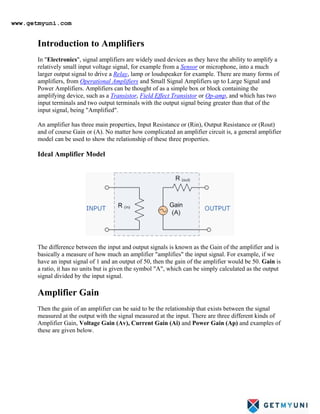
  • 1. Introduction to Amplifiers In "Electronics", signal amplifiers are widely used devices as they have the ability to amplify a relatively small input voltage signal, for example from a Sensor or microphone, into a much larger output signal to drive a Relay, lamp or loudspeaker for example. There are many forms of amplifiers, from Operational Amplifiers and Small Signal Amplifiers up to Large Signal and Power Amplifiers. Amplifiers can be thought of as a simple box or block containing the amplifying device, such as a Transistor, Field Effect Transistor or Op-amp An amplifier has three main properties, Input Resistance or (Rin), Output Resistance or (Rout) and of course Gain or (A). No matter how complicated an amplifier circuit is, a general amplifier model can be used to show the relationship of these three properties. , and which has two input terminals and two output terminals with the output signal being greater than that of the input signal, being "Amplified". Ideal Amplifier Model The difference between the input and output signals is known as the Gain of the amplifier and is basically a measure of how much an amplifier "amplifies" the input signal. For example, if we have an input signal of 1 and an output of 50, then the gain of the amplifier would be 50. Gain is a ratio, it has no units but is given the symbol "A", which can be simply calculated as the output signal divided by the input signal. Amplifier Gain Then the gain of an amplifier can be said to be the relationship that exists between the signal measured at the output with the signal measured at the input. There are three different kinds of Amplifier Gain, Voltage Gain (Av), Current Gain (Ai) and Power Gain (Ap) and examples of these are given below. www.getmyuni.com
  • 2. Amplifier Gain of the Input Signal Voltage Amplifier Gain Current Amplifier Gain Power Amplifier Gain Note that for the Power Gain you can also divide the power obtained at the output with the power obtained at the input. Also, the subscripts v, i and p denote the type of signal gain. The power Gain of the amplifier can also be expressed in Decibels, (dB). The Bel is a logarithmic unit (base 10) of measurement that has no units but as the Bel is a large unit of measure, it has be prefixed with deci making it Decibels with one decibel being one tenth (1/10th) of a Bel. To calculate the gain of the amplifier in Decibels or dB, we can use the following expressions. • Voltage Gain in dB: av = 20 log Av • • Current Gain in dB: ai = 20 log Ai • • Power Gain in dB: ap = 10 log Ap Note that the DC power gain of an amplifier is equal to ten times the common log of the output to input ratio, where as voltage and current gains are 20 times the common log of the ratio. Also, a positive value of dB represents a Gain and a negative value of dB represents a Loss within the www.getmyuni.com
  • 3. amplifier. For example, an amplifier gain of +3dB indicates that the output signal has "doubled", (x2) while an amplifier gain of -3dB indicates that the signal has "halved", (x0.5) or in other words a loss. Example No1 Determine the Voltage, Current and Power Gain of an amplifier that has an input signal of 1mA at 10mV and a corresponding output signal of 10mA at 1V. Also, express all three gains in decibels, (dB). Amplifier Gain. in Decibels (dB). Then the amplifier has a Voltage Gain of 100, a Current Gain of 10 and a Power Gain of 1,000. Amplifiers can be divide into two distinct types, Small Signal Amplifiers such as pre- amplifiers, instrumentation amplifiers etc, which are designed to amplify very small signal voltage levels of only a few micro-volts (μV) from sensors or audio signals and Large Signal Amplifiers such as audio power amplifiers or switching amplifiers, which are designed to amplify large input voltage signals or switch high current loads. Power Amplifiers Small signal amplifiers are generally referred to as "Voltage" amplifiers as they convert a small input voltage into a much larger output voltage. Sometimes an amplifier is required to drive a www.getmyuni.com
  • 4. motor or feed a loudspeaker and for these types of applications where high switching currents are needed Power Amplifiers are required. The main function of Power amplifiers (also known as large signal amplifiers) is to deliver power, which as we know from above, is the product of the voltage and current applied to the load. The power amplifier works on the basic principle of converting the DC power drawn from the power supply into an AC voltage signal delivered to the load. Although the amplification is high the efficiency of the conversion from the DC power supply input to the AC voltage signal output is usually poor. The perfect or ideal amplifier would give us an efficiency rating of 100% or at least the power IN is equal to the power OUT. However, this can never happen as some of its power is lost in the form of heat and also, the amplifier itself consumes power during the amplification process. Then the efficiency of an amplifier is given as: Amplifier Efficiency Amplifier Classes We saw in the Common Emitter Audio Power Amplifiers are classified in order according to their circuit configurations and mode of operation being designated different classes of operation in alphabetical order such as A, B, C, AB, etc. These different classes of operation range from a near linear output but with low efficiency to a non-linear output but with a high efficiency. There are typical maximum efficiencies for the various types or class of amplifier, with the most commonly used being: transistor tutorial that for the transistor to operate within its "Active Region" some form of "Base Biasing" was required. This small Base Bias voltage added to the input signal allowed the transistor to reproduce the full input waveform at its output with no loss of signal. However, by altering the position of this Base Bias voltage, it is possible to operate an amplifier in an amplification mode other than that for full waveform reproduction. By changing the amplifiers Base bias voltage different ranges or modes of operation can be obtained and these are categorized according to their Class. • Class A - a maximum theoretical efficiency of less than 40% • • Class B - with a maximum theoretical efficiency of about 70% • • Class AB - which an efficiency rating between that of Class A and Class B Class A Operation Class A Amplifier operation is were the entire input signal waveform is faithfully reproduced at the amplifiers output as the transistor is perfectly biased within its active region, thereby never www.getmyuni.com
  • 5. reaching either of its Cut-off or Saturation regions. This then results in the AC input signal being perfectly "centered" between the amplifiers upper and lower signal limits as shown below. Class A Output Waveform Here, the Class A amplifier uses the same transistor for both halves of the output waveform and due to its biasing arrangement always has current flowing through it, even if there is no input signal. In other words the output transistors never turns "OFF". This results in the class A type of operation being very inefficient as its conversion of the DC supply power to the AC signal power delivered to the load is usually very low. Generally, the output transistor of a Class A amplifier gets very hot even when there is no input signal present so some form of heatsinking is required. The DC current flowing through the output transistor (Ic) when there is no output signal will be equal to the current flowing through the load. Class B Operation Unlike the Class A amplifier above that uses a single transistor for its output stage, the Class B Amplifier uses two complimentary transistors (an NPN and a PNP) for each half of the output waveform. One transistors for the positive half of the waveform and another for the negative half of the waveform. This means that each transistor spends half of its time in the Active region and half its time in the Cut-off region. Class B operation has no DC bias voltage instead the transistor only conducts when the input signal is greater than the base-emitter voltage and for silicon devices is about 0.7v. Therefore, at zero input there is zero output. This then results in only half the input signal being presented at the amplifiers output giving a greater efficiency as shown below. Class B Output Waveform www.getmyuni.com
  • 6. As the output transistors for each half of the waveform, both positive and negative, requires a base-emitter voltage greater than the 0.7v required for the bipolar transistor to start conducting, the lower part of the output waveform which is below this 0.7v window will not be reproduced accurately resulting in a distorted area of the output waveform as one transistor turns "OFF" waiting for the other to turn back "ON". This type of distortion is called Crossover Distortion and is looked at later on in this section. Class AB Operation The Class AB Amplifier is a compromise between the Class A and the Class B configurations above. While Class AB operation still uses two complementary transistors in its output stage a very small biasing voltage is applied to the Base of the transistor to bias it close to the Cut-off region when no input signal is present. An input signal will cause the transistor to operate as normal in its Active region thereby eliminating any crossover distortion. A small Collector current will flow when there is no input signal but it is much less than that for the Class A amplifier configuration. This means then that the transistor will be "ON" for more than half a cycle of the waveform. This type of amplifier configuration improves both the efficiency and linearity of the amplifier circuit compared to Class A. Class AB Output Waveform www.getmyuni.com
  • 7. The class of operation for an amplifier is very important as it determines both the efficiency and the amount of power that the amplifier consumes and dissipates in the form of wasted heat, which may also require larger power transistors, more expensive heatsinks, cooling fans, or even an increase in the size of the power supply required to deliver the extra power required by the amplifier. Power converted into heat from transistors, resistors or any other component makes any electronic circuit inefficient and will result in premature failure of the device. So why use a Class A amplifier if its efficiency is less than 40% compared to a Class B amplifier that has a higher efficiency rating of nearly 70%. Basically, a Class A amplifier gives a more linear output meaning that it has, Linearity over a larger frequency response. The Common Emitter Amplifier In the Transistor tutorial We also saw that a static or DC load line can be drawn onto these output characteristics curves to show all the possible operating points of the transistor from fully "ON" to fully "OFF", and to which the quiescent operating point or Q-point of the amplifier can be found. The aim of any small signal amplifier is to amplify all of the input signal with the minimum amount of distortion possible to the output signal, in other words, the output signal must be an exact reproduction of the input signal but only bigger (amplified). To obtain low distortion when used as an amplifier we saw that the most common circuit configuration for a transistor is that of the Common Emitter Amplifier and that a family of curves known commonly as the Output Characteristics Curves, relates the Collector current (Ic), to the output or Collector voltage (Vce), for different values of Base current (Ib) signal. All types of signal amplifiers operate using AC signal inputs which alternate between a positive value and a negative value so some way of presetting the amplifier circuit to operate between these two maximum or peak values is required. This is achieved using a process known as Biasing. Biasing is very important in amplifier design as it establishes the correct operating point of the amplifier ready to receive signals, thereby reducing any distortion to the input signal. www.getmyuni.com
  • 8. the operating quiescent point needs to be correctly selected. This is in fact the DC operating point of the amplifier and its position may be established at any point along the load line by a suitable biasing arrangement. The best possible position for this Q-point is as close to the centre position of the load line as reasonably possible, thereby producing a Class A type amplifier operation, ie. Vce = 1/2Vcc. Consider the Common Emitter Amplifier circuit shown below. The Common Emitter Amplifier Circuit The amplifier circuit shown above uses what is commonly called "Voltage Divider Biasing". This type of biasing arrangement is commonly used in the design of bipolar transistor amplifier circuits and which greatly reduces the effects of varying Beta, (β) by holding the Base bias at a constant steady voltage allowing for best stability. The quiescent Base voltage (Vb) is determined by the potential divider network formed by the two resistors, R1 and R2 and the power supply voltage Vcc. The voltage level generated at the junction of resistors R1 and R2 holds the Base voltage (Vb) constant at a value below the supply voltage. This reference voltage can be easily calculated using the simple voltage divider formula: This same supply voltage, (Vcc) also determines the maximum Collector current, Ic when the transistor is switched fully "ON" (saturation), Vce = 0. The Base current Ib for the transistor is found from the Collector current, Ic and the DC current gain Beta, β of the transistor. www.getmyuni.com
  • 9. Beta is sometimes referred to as hFE which is the transistors forward current gain in the common emitter configuration. Beta has no units as it is a fixed ratio of the two currents, Ic and Ib so a small change in the Base current will cause a large change in the Collector current. One final point about Beta. Transistors of the same type and part number will have large variations in their Beta value for example, the BC107 NPN Bipolar transistor has a DC current gain Beta value of between 110 and 450 (data sheet value) this is because Beta is a characteristic of their construction. As the Base/Emitter junction is forward-biased, the Emitter voltage, Ve will be one junction voltage drop different to the Base voltage. If the voltage across the Emitter resistor is known then the Emitter current, Ie can be easily calculated using Ohm's Law Example No1 . The Collector current, Ic can be approximated, since it is almost the same value as the Emitter current. Assuming a load resistor, RL of 1.2kΩs and a supply voltage of 12v. Calculate the maximum Collector current (Ic) flowing through the load resistor when the transistor is switched fully "ON", assume Vce = 0. Also find the value of the Emitter resistor, RE with a voltage drop of 1v across it and the values of all the other resistors assuming a silicon transistor. This then establishes point "A" on the Collector current vertical axis of the characteristics curves and occurs when Vce = 0. When the transistor is switched fully "OFF", their is no voltage drop across either resistor RE or RL as no current is flowing through them. Then the voltage drop across the transistor, Vce is equal to the supply voltage, Vcc. This then establishes point "B" on the horizontal axis of the characteristics curves. Generally, the quiescent Q-point of the amplifier is with zero input signal applied to the Base, so the Collector sits half-way along the load line between zero volts and the supply voltage, (Vcc/2). Therefore, the Collector current at the Q- point of the amplifier will be given as: This static DC load line produces a straight line equation whose slope is given as: -1/(RL + RE) and that it crosses the vertical Ic axis at a point equal to Vcc/(RL + RE). The actual position of the Q-point on the DC load line is determined by the mean value of Ib. www.getmyuni.com
  • 10. As the Collector current, Ic of the transistor is also equal to the DC gain of the transistor (Beta), times the Base current (β x Ib), if we assume a Beta (β) value for the transistor of say 100, (one hundred is a reasonable average value for low power signal transistors) the Base current Ib flowing into the transistor will be given as: Instead of using a separate Base bias supply, it is usual to provide the Base Bias Voltage from the main supply rail (Vcc) through a dropping resistor, R1. Resistors, R1 and R2 can now be chosen to give a suitable quiescent Base current of 45.8μA or 46μA rounded off. The current flowing through the potential divider circuit has to be large compared to the actual Base current, Ib, so that the voltage divider network is not loaded by the Base current flow. A general rule of thumb is a value of at least 10 times Ib flowing through the resistor R2. Transistor Base/Emitter voltage, Vbe is fixed at 0.7V (silicon transistor) then this gives the value of R2 as: If the current flowing through resistor R2 is 10 times the value of the Base current, then the current flowing through resistor R1 in the divider network must be 11 times the value of the Base current. The voltage across resistor R1 is equal to Vcc - 1.7v (VRE + 0.7 for silicon transistor) which is equal to 10.3V, therefore R1 can be calculated as: The value of the Emitter resistor, RE can be easily calculated using Ohm's Law. The current flowing through RE is a combination of the Base current, Ib and the Collector current Ic and is given as: Resistor, RE is connected between the Emitter and ground and we said previously that it has a voltage of 1 volt across it. Then the value of RE is given as: www.getmyuni.com
  • 11. So, for our example above, the preferred values of the resistors chosen to give a tolerance of 5% (E24) are: Then, our original Common Emitter circuit above can be rewritten to include the values of the components that we have just calculated. Completed Common Emitter Circuit Coupling Capacitors In common emitter amplifier circuits, capacitors C1 and C2 are used as Coupling Capacitors to separate the AC signals from the DC bias. This ensures that the bias condition set up for the circuit to operate correctly is not effected by any additional amplifier stages, as the capacitors will only pass AC signals and block any DC component. The output AC signal is then superimposed on the biasing of the following stages. Also a bypass capacitor, CE is included in the Emitter leg circuit. This capacitor is an open circuit component for DC bias meaning that the biasing currents and voltages are not affected by the addition of the capacitor maintaining a good Q-point stability. However, this bypass capacitor short circuits the Emitter resistor at high frequency signals and only RL plus a very small internal resistance acts as the transistors load increasing the voltage gain to its maximum. Generally, the value of the bypass capacitor, CE is www.getmyuni.com
  • 12. chosen to provide a reactance of at most, 1/10th the value of RE at the lowest operating signal frequency. Output Characteristics Curves Ok, so far so good. We can now construct a series of curves that show the Collector current, Ic against the Collector/Emitter voltage, Vce with different values of Base current, Ib for our simple common emitter amplifier circuit. These curves are known as the "Output Characteristic Curves" and are used to show how the transistor will operate over its dynamic range. A static or DC load line is drawn onto the curves for the load resistor RL of 1.2kΩ to show all the transistors possible operating points. When the transistor is switched "OFF", Vce equals the supply voltage Vcc and this is point B on the line. Likewise when the transistor is fully "ON" and saturated the Collector current is determined by the load resistor, RL and this is point A on the line. We calculated before from the DC gain of the transistor that the Base current required for the mean position of the transistor was 45.8μA and this is marked as point Q on the load line which represents the Quiescent point or Q-point of the amplifier. We could quite easily make life easy for ourselves and round off this value to 50μA exactly, without any effect to the operating point. Output Characteristics Curves www.getmyuni.com
  • 13. Point Q on the load line gives us the Base current Q-point of Ib = 45.8μA or 46μA. We need to find the maximum and minimum peak swings of Base current that will result in a proportional change to the Collector current, Ic without any distortion to the output signal. As the load line cuts through the different Base current values on the DC characteristics curves we can find the peak swings of Base current that are equally spaced along the load line. These values are marked as points N and M on the line, giving a minimum and a maximum Base current of 20μA and 80μA respectively. These points, N and M can be anywhere along the load line that we choose as long as they are equally spaced from Q. This then gives us a theoretical maximum input signal to the Base terminal of 30μA peak-to-peak without producing any distortion to the output signal. Any input signal giving a Base current greater than this value will drive the transistor to go beyond point N and into its Cut-off region or beyond point M and into its Saturation region thereby resulting in distortion to the output signal in the form of "clipping". Using points N and M as an example, the instantaneous values of Collector current and corresponding values of Collector-emitter voltage can be projected from the load line. It can be www.getmyuni.com
  • 14. seen that the Collector-emitter voltage is in anti-phase (-180o ) with the collector current. As the Base current Ib changes in a positive direction from 50μA to 80μA, the Collector-emitter voltage, which is also the output voltage decreases from its steady state value of 5.8v to 2.0v. Then a single stage Common Emitter Amplifier is also an "Inverting Amplifier" as an increase in Base voltage causes a decrease in Vout and a decrease in Base voltage produces an increase in Vout. Voltage Gain The Voltage Gain of the common emitter amplifier is equal to the ratio of the change in the input voltage to the change in the amplifiers output voltage. Then ΔVL is Vout and ΔVB is Vin. But voltage gain is also equal to the ratio of the signal resistance in the Collector to the signal resistance in the Emitter and is given as: We mentioned earlier that as the signal frequency increases the bypass capacitor, CE starts to short out the Emitter resistor. Then at high frequencies RE = 0, making the gain infinite. However, bipolar transistors have a small internal resistance built into their Emitter region called Re. The transistors semiconductor material offers an internal resistance to the flow of current through it and is generally represented by a small resistor symbol shown inside the main transistor symbol. Transistor data sheets tell us that for a small signal bipolar transistors this internal resistance is the product of 25mV ÷ Ie (25mV being the internal volt drop across the Base/Emitter junction depletion layer), then for our common Emitter amplifier circuit above this resistance value will be equal to: This internal Emitter leg resistance will be in series with the external Emitter resistor, RE, then the equation for the transistors actual gain will be modified to include this internal resistance and is given as: At low frequency signals the total resistance in the Emitter leg is equal to RE + Re. At high frequency, the bypass capacitor shorts out the Emitter resistor leaving only the internal resistance Re in the Emitter leg resulting in a high gain. Then for our common emitter amplifier circuit above, the gain of the circuit at both low and high signal frequencies is given as: www.getmyuni.com
  • 15. At Low Frequencies At High Frequencies One final point, the voltage gain is dependent only on the values of the Collector resistor, RL and the Emitter resistance, (RE + Re) it is not affected by the current gain Beta, β (hFE) of the transistor. So, for our simple example above we can now summarise all the values we have calculated for our common emitter amplifier circuit and these are: Minimum Mean Maximum Base Current 20μA 50μA 80μA Collector Current 2.0mA 4.8mA 7.7mA Output Voltage Swing 2.0V 5.8V 9.3V Amplifier Gain -5.32 -218 Summary Then to summarize, The Common Emitter Amplifier circuit has a resistor in its Collector circuit. The current flowing through this resistor produces the voltage output of the amplifier. The value of this resistor is chosen so that at the amplifiers quiescent operating point, Q-point this output voltage lies half way along the transistors load line. The Base of the transistor used in a common Emitter amplifier is biased using two resistors as a potential divider network. This type of biasing arrangement is commonly used in the design of bipolar transistor amplifier circuits and greatly reduces the effects of varying Beta, (β) by holding the Base bias at a constant steady voltage. This type of biasing produces the greatest stability. A resistor can be included in the Emitter leg in which case the voltage gain becomes -RL/RE. If there is no external Emitter resistance, the voltage gain of the amplifier is not infinite as there is a very small internal resistance, Re in the Emitter leg. The value of this internal resistance is equal to 25mV/IE www.getmyuni.com
  • 16. RESET JFET Amplifier So far we have looked at the Bipolar type amplifiers and especially the Common Emitter amplifier, but small signal amplifiers can also be made using Field Effect Transistors or FET's. These devices have the advantage over bipolar devices of having an extremely high input impedance along with a low noise output making them very useful in amplifier circuits using very small signals. The design of an amplifier circuit based around a JFET (n-channel FET for this example) or even a MOSFET is exactly the same principle as that for a bipolar device and for a Class A amplifier as we looked at in the previous tutorial. A suitable Quiescent point still needs to be found for the correct biasing of the amplifier circuit with amplifier configurations of Common Source, Common Drain and Common Gate available for FET devices. In this tutorial we will look at the JFET Amplifier as a common source amplifier as this is the most widely used design. Consider the Common Source JFET Amplifier circuit below. Common Source JFET Amplifier The circuit consists of an N-channel JFET, but the device could also be an equivalent N-channel Depletion-mode MOSFET as the circuit diagram would be the same, just a change in the FET. The JFET Gate voltage Vg is biased through the potential divider network set up by resistors R1 and R2 and is biased to operate within its saturation region which is equivalent to the active region of the BJT. The Gate biasing voltage Vg is given as: www.getmyuni.com
  • 17. Note that this equation only determines the ratio of the resistors R1 and R2, but in order to take advantage of the very high input impedance of the JFET as well as reducing the power dissipation within the circuit, we need to make these resistor values as high as possible, with values in the order of 1 to 10MΩ being common. The input signal, (Vin) is applied between the Gate terminal and 0v with the Drain circuit containing the load resistor, Rd. The output voltage, Vout is developed across this load resistance. There is also an additional resistor, Rs included in the Source lead and the same Drain current also flows through this resistor. When the JFET is switched fully "ON" a voltage drop equal to Rs x Id is developed across this resistor raising the potential of the Source terminal above 0v or ground level. This voltage drop across Rs due to the Drain current provides the necessary reverse biasing condition across the Gate resistor, R2. In order to keep the Gate-source junction reverse biased, the Source voltage, Vs needs to be higher than the gate voltage, Vg. This Source voltage is therefore given as: Then the Drain current, Id is also equal to the Source current, Is as "No Current" enters the Gate terminal and this can be given as: This potential divider biasing circuit improves the stability of the common source JFET circuit when being fed from a single DC supply compared to that of a fixed voltage biasing circuit. Both Resistor, Rs and Capacitor, Cs serve basically the same function as the Emitter resistor and capacitor in the Common Emitter Bipolar Transistor amplifier circuit, namely to provide good stability and prevent a reduction in the signal gain. However, the price paid for a stabilized quiescent Gate voltage is that more of the supply voltage is dropped across Rs. The basic circuit and characteristics of a common source JFET amplifier are very similar to that of the Common Emitter amplifier. A DC load line is constructed by joining the two points relating to the Drain current, Id and the supply voltage, Vdd intersecting the curves at the Q- point as follows. JFET Amplifier Characteristics Curves www.getmyuni.com
  • 18. As with the Common Emitter circuit, the DC load line produces a straight line equation whose gradient is given as: -1/(Rd + Rs) and that it crosses the vertical Id axis at a point equal to Vdd/(Rd + Rs). The other end of the load line crosses the horizontal axis at a point equal to Vdd. The actual position of the Q-point on the DC load line is determined by the mean value of Vg which is biased negatively as the JFET as a depletion-mode device. Like the bipolar common emitter amplifier the output of the Common Source JFET Amplifier is 1800 out of phase with the input signal. One of the main disadvantages of using Depletion-mode JFET is that they need to be negatively biased. Should this bias fail for any reason the Gate-source voltage may rise and become positive causing an increase in Drain current resulting in failure of the Drain voltage, Vd. Also the high channel resistance, Rds(on) of the JFET, coupled with high quiescent steady state Drain current makes these devices run hot so additional heatsink is required. However, most of the problems associated with using JFET's can be greatly reduced by using enhancement-mode MOSFET devices instead. www.getmyuni.com
  • 19. MOSFETs Amplifier Distortion or Metal Oxide Semiconductor FET's have much higher input impedances and low channel resistances compared to the equivalent JFET. Also the biasing arrangements for MOSFETs are different and unless we bias them positively for N-channel devices and negatively for P-channel devices no Drain current will flow, then we have in effect a fail safe transistor. From the previous tutorials we learnt that for a signal amplifier to work correctly it requires some form of DC Bias on its Base or Gate terminal so that it amplifies the input signal over its entire cycle with the bias Q-point set as near to the middle of the load line as possible. This then gave us a Class "A" type amplification with the most common configuration being Common Emitter for Bipolar transistors and Common Source for unipolar transistors. We also saw that the Power, Voltage or Current Gain, (amplification) provided by the amplifier is the ratio of the peak input value to its peak output value. However, if we incorrectly design our amplifier circuit and set the biasing Q-point at the wrong position on the load line or apply too large an input signal, the resultant output signal may not be an exact reproduction of the original input signal waveform. Consider the common emitter amplifier circuit below. Common Emitter Amplifier Distortion of the signal waveform may take place because: • 1. Amplification may not be taking place over the whole signal cycle due to incorrect biasing. • • 2. The input may be too large, causing the amplifier to limit. • • 3. The amplification may not be linear over the entire frequency range of inputs. www.getmyuni.com
  • 20. This means then that during the amplification process of the signal waveform, some form of Amplifier Distortion has occurred. Amplitude Distortion Amplifiers are basically designed to amplify small voltage input signals into much larger output signals and this means that the output signal is constantly changing by some factor or value times the input signal at all input frequencies. We saw previously that this multiplication factor is called the Beta, β value of the transistor. Common Emitter or even common Source type circuits work fine for small AC input signals but suffer from one major disadvantage, the bias Q-point of a bipolar amplifier depends on the same Beta value which may vary from transistors of the same type, ie. the Q-point for one transistor is not necessarily the same as the Q-point for another transistor of the same type due to the inherent manufacturing tolerances. If this occurs the amplifier may not be linear and Amplitude Distortion will result but careful choice of the transistor can minimise this effect. Amplitude distortion occurs when the peak values of the frequency waveform are attenuated causing distortion due to a shift in the Q-point and amplification may not take place over the whole signal cycle. This non-linearity of the output waveform is shown below. Amplitude Distortion due to Incorrect Biasing If the bias is correct the output waveform should look like that of the input waveform only bigger, (amplified). If there is insufficient bias the output waveform will look like the one on the right with the negative part of the output waveform "cut-off". If there is too much bias the output waveform will look like the one on the left with the positive part "cut-off". When the bias voltage is too small, during the negative part of the cycle the transistor does not conduct fully so the output is set by the supply voltage. When the bias is too great the positive part of the cycle saturates the transistor and the output drops almost to zero. www.getmyuni.com
  • 21. Even with the correct biasing voltage level set, it is still possible for the output waveform to become distorted due to a large input signal being amplified by the circuits gain. The output voltage signal becomes clipped in both the positive and negative parts of the waveform an no longer resembles a sine wave, even when the bias is correct. This type of amplitude distortion is called Clipping and is the result of "Over-driving" the input of the amplifier. When the input amplitude becomes too large, the clipping becomes substantial and forces the output waveform signal to exceed the power supply voltage rails with the peak (+ve half) and the trough (-ve half) parts of the waveform signal becoming flattened or "Clipped-off". To avoid this the maximum value of the input signal must be limited to a level that will prevent this clipping effect as shown above. Amplitude Distortion due to Clipping Amplitude Distortion greatly reduces the efficiency of an amplifier circuit. These "flat tops" of the distorted output waveform either due to incorrect biasing or over driving the input do not contribute anything to the strength of the output signal at the desired frequency. Having said all that, some well known guitarist and rock bands actually prefer that their distinctive sound is highly distorted or "overdriven" by heavily clipping the output waveform to both the +ve and -ve power supply rails. Also, excessive amounts of clipping can also produce an output which resembles a "square wave" shape which can then be used in electronic or digital circuits. We have seen that with a DC signal the level of gain of the amplifier can vary with signal amplitude, but as well as Amplitude Distortion, other types of distortion can occur with AC signals in amplifier circuits, such as Frequency Distortion and Phase Distortion. Frequency Distortion Frequency Distortion occurs in a transistor amplifier when the level of amplification varies with frequency. Many of the input signals that a practical amplifier will amplify consist of the required signal waveform called the "Fundamental Frequency" plus a number of different www.getmyuni.com
  • 22. frequencies called "Harmonics" superimposed onto it. Normally, the amplitude of these harmonics are a fraction of the fundamental amplitude and therefore have very little or no effect on the output waveform. However, the output waveform can become distorted if these harmonic frequencies increase in amplitude with regards to the fundamental frequency. For example, consider the waveform below: Frequency Distortion due to Harmonics In the example above, the input waveform consists a the fundamental frequency plus a second harmonic signal. The resultant output waveform is shown on the right hand side. The frequency distortion occurs when the fundamental frequency combines with the second harmonic to distort the output signal. Harmonics are therefore multiples of the fundamental frequency and in our simple example a second harmonic was used. Therefore, the frequency of the harmonic is 2 times the fundamental, 2 x f or 2f. Then a third harmonic would be 3f, a fourth, 4f, and so on. Frequency distortion due to harmonics is always a possibility in amplifier circuits containing reactive elements such as capacitance or inductance. Phase Distortion Phase Distortion or Delay Distortion occurs in a non-linear transistor amplifier when there is a time delay between the input signal and its appearance at the output. If we call the phase change between the input and the output zero at the fundamental frequency, the resultant phase angle delay will be the difference between the harmonic and the fundamental. This time delay will depend on the construction of the amplifier and will increase progressively with frequency within the bandwidth of the amplifier. For example, consider the waveform below: Phase Distortion due to Delay www.getmyuni.com
  • 23. Any practical amplifier will have a combination of both "Frequency" and "Phase" distortion together with amplitude distortion but in most applications such as in audio amplifiers or power amplifiers, unless the distortion is excessive or severe it will not generally affect the operation of the system. Class A Amplifier Common emitter voltage amplifiers are the most commonly used type of amplifier as they have a large voltage gain. They are designed to produce a large output voltage swing from a relatively small input signal voltage of only a few millivolt's and are used mainly as "Small Signal Amplifiers" as we saw in the previous tutorials. However, sometimes an amplifier is required to drive large resistive loads such as a loudspeaker and for these types of applications where high switching currents are needed Power Amplifiers are required. The main function of the Power amplifier, which are also known as a "Large Signal Amplifier" is to deliver power, which is the product of voltage and current to the load. Basically a power amplifier is also a voltage amplifier the difference being that the load resistance connected to the output is relatively low, for example a loudspeaker of 4 or 8Ωs resulting in high currents flowing through the Collector of the transistor. Because of these high load currents the output transistor(s) used for power amplifier output stages need to have higher voltage and power ratings than the general ones used for small signal stages. Since we are interested in delivering maximum AC power to the load, while consuming the minimum DC power possible from the supply we are mostly concerned with the "Conversion Efficiency" of the amplifier. However, one of the main disadvantage of power amplifiers and especially Class A type amplifiers is that their overall conversion efficiency is very low. Percentage efficiency in amplifiers is defined as the r.m.s. output power dissipated in the load divided by the total DC power taken from the supply source as shown below. Power Amplifier Efficiency www.getmyuni.com
  • 24. • Where: • • η% - is the efficiency of the amplifier. • • Pout - is the amplifiers output power delivered to the load. • • Pdc - is the DC power taken from the supply. For a power amplifier it is very important that the amplifiers power supply is well designed to provide the maximum available continuous power to the output signal. Class A Amplifier The most commonly used type of power amplifier configuration is the Class A Amplifier. Class A amplifier stages use the transistor in the standard Common Emitter circuit configuration as seen previously, in which the transistor is always biased "ON" so that it conducts during one complete cycle of the input signal waveform producing minimum distortion to the output. This means then that the Class A Amplifier configuration is the ideal operating mode, because there can be no crossover or switch-off distortion to the output waveform. Class A power amplifier output stages may use a single transistor or pairs of transistors connected together to share the high load current. Consider the Class A amplifier circuit below. Single-ended Amplifier Circuit www.getmyuni.com
  • 25. This is the simplest type of Class A power amplifier circuit. It uses a single-ended transistor for its output stage with the resistive load connected directly to the Collector terminal. When the transistor switches "ON" it sinks the output current through the Collector resulting in an inevitable voltage drop across the Emitter resistance thereby limiting the negative output capability. The efficiency of this type of circuit is very low (possibly 20%) and delivers small power outputs for a large drain on the DC power supply. A Class A amplifier stage passes the same load current even when no input signal is applied so large heatsinks are needed for the output transistors. However, another simple way to increase the current handling capacity of the circuit while at the same time obtain a greater power gain is to replace the single output transistor with a Darlington Transistor. These types of devices are basically two transistors within a single package, one small "pilot" transistor and another larger "switching" transistor. The big advantage of these devices are that the input impedance is suitably large while the output impedance is relatively low, thereby reducing the power loss and therefore the heat within the switching device. Darlington Transistor Configurations www.getmyuni.com
  • 26. The overall current gain Beta (β) or Hfe value of a Darlington device is the product of the two individual gains of the transistors multiplied together and very high β values along with high Collector currents are possible compared to a single transistor circuit. To improve the full power efficiency of the Class A amplifier it is possible to design the circuit with a transformer connected directly in the Collector circuit to form a circuit called a Transformer Coupled Amplifier. This improves the efficiency of the amplifier by matching the impedance of the load with that of the amplifiers output using the turns ratio (N) of the transformer and an example is given below. Transformer-coupled Amplifier Circuit www.getmyuni.com
  • 27. As the Collector current, Ic is reduced to below the quiescent Q-point set up by the Base bias voltage, due to variations in the Base current, the magnetic flux in the transformer core collapses causing an induced emf in the transformer primary windings. This causes an instantaneous Collector voltage to rise to a value of twice the supply voltage 2Vcc giving a maximum Collector current of twice Ic when the Collector voltage is at its minimum. Then the efficiency of this type of Class A amplifier configuration can be calculated as follows. The r.m.s. Collector voltage is given as: The r.m.s. Collector current is given as: The r.m.s. Power delivered to the load (Pac) is therefore given as: The average power drawn from the supply (Pdc) is given by: and therefore the efficiency of a Transformer-coupled Class A amplifier is given as: This improves the efficiency of the amplifier by matching the impedance of the load with that of the amplifier using the turns ratio of the transformer and efficiencies reaching 40% are possible with most commercially available Class-A type power amplifiers of this type of configuration, but the use of inductive components is best avoided. Also one big disadvantage of this type of circuit is the additional cost and size of the audio transformer required. It is possible to obtain greater power output and efficiency than that of a Class A amplifier by using two transistors in the output stage in a "push-pull" configuration. This type of configuration is called a Class B Amplifier which we will look at in the next tutorial. www.getmyuni.com
  • 28. Class B Amplifiers To improve the full power efficiency of the previous Class A type amplifier it is possible to design the amplifier circuit with two transistors in its output stage producing a "push-pull" type amplifier configuration. Push-pull operation uses two "complementary" transistors, one an NPN- type and the other a PNP-type with both power transistors receiving the same input signal together that is equal in magnitude, but in opposite phase to each other. This results in one transistor only amplifying one half or 1800 of the input waveform while the other transistor amplifies the other half or remaining 1800 of the waveform with the resulting "two-halves" being put back together at the output terminal. This pushing and pulling of the alternating half cycles by the transistors gives this type of circuit its name but they are more commonly known as Class B Amplifiers as shown below. Class B Push-pull Transformer Amplifier Circuit The circuit above shows a standard push-pull amplifier circuit that uses a balanced centre-tapped input transformer, which splits the incoming waveform signal into two equal cycles that are 1800 out of phase with each other and another centre-tapped transformer on the output to recombined the signals and provide the increased power to the load. The transistors used for this type of transformer push-pull amplifier circuit are both NPN transistors with their emitter terminals connected together. Here, the load current is shared between the two power transistor devices as it decreases in one device and increases in the other throughout the signal cycle reducing the www.getmyuni.com
  • 29. output voltage and current to zero. The result is that both halves of the output waveform now swings from zero to twice the quiescent current thereby reducing dissipation. This has the effect of almost doubling the efficiency of the amplifier to around 70%. Assuming that no input signal is present, then each transistor carries the normal quiescent collector current, the value of which is determined by the base bias which is at the cut-off point. If the transformer is accurately centre tapped, then the two collector currents will flow in opposite directions (ideal condition) and there will be no magnetization of the transformer core, thus minimizing the possibility of distortion. When a signal is present across the secondary of the driver transformer T1, the transistor base inputs are in "anti-phase" to each other as shown, thus if TR1 base goes positive driving the transistor into heavy conduction, its collector current will increase but at the same time the base current of TR2 will go negative further into cut-off and the collector current of this transistor decreases by an equal amount and vice versa. Hence negative halves are amplified by one transistor and positive halves by the other transistor giving this push- pull effect. Unlike the DC condition, these AC currents are ADDITIVE resulting in the two output half-cycles being combined to reform the sine-wave in the output transformers primary winding which then appears across the load. Class B Amplifier operation has zero DC bias as the transistors are biased at the cut-off, so each transistor only conducts when the input signal is greater than the base-emitter voltage. Therefore, at zero input there is zero output. This then means that the actual Q-point of a Class B amplifier is on the Vce part of the load line as shown below. Class B Output Characteristics Curves www.getmyuni.com
  • 30. Class B Amplifiers have the advantage over their Class A amplifier cousins in that no current flows through the transistors when they are in their quiescent state (ie, with no input signal), therefore no power is dissipated in the output transistors or transformer when there is no signal present unlike Class A amplifier stages that require significant base bias thereby dissipating lots of heat - even with no input signal. So the overall conversion efficiency ( η ) of the amplifier is greater than that of the equivalent Class A with efficiencies reaching as high as 75% possible resulting in nearly all modern types of push-pull amplifiers operated in this Class B mode. Transformerless Class B Push-Pull Amplifier One of the main disadvantages of the Class B amplifier circuit above is that it uses balanced centre-tapped transformers in its design, making it expensive to construct. However, there is another type of Class B push-pull amplifier called a Complementary-Symmetry Class B Amplifier that does not use transformers in its design therefore, it is transformerless using instead complementary pairs of transistors. As transformers are not needed this makes the amplifier circuit much smaller for the same amount of output, also there are no stray magnetic effects or transformer distortion to effect the quality of the output signal. An example of a "transformerless" circuit is given below. www.getmyuni.com
  • 31. Class B Transformerless Output Stage While Class B amplifiers have a much high gain than the Class A types, one of the main disadvantages of class B type push-pull amplifiers is that they suffer from an effect known commonly as Crossover Distortion Transformerless Class AB Push-Pull Amplifier . This occurs during the transition when the transistors are switching over from one to the other as each transistor does not stop or start conducting exactly at the zero crossover point even if they are specially matched pairs. This is because the output transistors require a base-emitter voltage greater than 0.7v for the bipolar transistor to start conducting which results in both transistors being "OFF" at the same time. One way to eliminate this crossover distortion effect would be to bias both the transistors at a point slightly above their cut-off point. This then would give us what is commonly called an Class AB Amplifier circuit. We know that we need the base-emitter voltage to be greater than 0.7v for a silicon bipolar transistor to start conducting, so if we were to replace the two voltage divider biasing resistors connected to the base terminals of the transistors with two silicon Diodes Class AB Amplifier , the biasing voltage applied to the transistors would now be equal to the forward voltage drop of the diode. These two diodes are generally called Biasing Diodes or Compensating Diodes and are chosen to match the characteristics of the matching transistors. The circuit below shows diode biasing. www.getmyuni.com
  • 32. The Class AB Amplifier circuit is a compromise between the Class A and the Class B configurations. This very small diode biasing voltage causes both transistors to slightly conduct even when no input signal is present. An input signal waveform will cause the transistors to operate as normal in their active region thereby eliminating any crossover distortion. A small collector current will flow when there is no input signal but it is much less than that for the Class A amplifier configuration. This means then that the transistor will be "ON" for more than half a cycle of the waveform but much less than a full cycle. The amount of diode biasing voltage present at the base terminal of the transistor can also be increased in multiples by adding additional diodes in series. Crossover Distortion We have seen that one of the main disadvantages of a Class A Amplifier is its low full power efficiency rating. But we also know that we can improve the amplifier and almost double its efficiency simply by changing the output stage of the amplifier to a Class B push-pull type configuration. However, this is great from an efficiency point of view, but most modern Class B amplifiers are transformerless or complementary types with two transistors in their output stage. This results in one main fundamental problem with push-pull amplifiers in that the two transistors do not combine together fully at the output both halves of the waveform due to their unique zero cut-off biasing arrangement. As this problem occurs when the signal changes or "crosses-over" from one transistor to the other at the zero voltage point it produces an amount of "distortion" to the output wave shape. This results in a condition that is commonly called Crossover Distortion. Crossover Distortion produces a zero voltage "flat spot" or "deadband" on the output wave shape as it crosses over from one half of the waveform to the other. The reason for this is that the www.getmyuni.com
  • 33. transition period when the transistors are switching over from one to the other, does not stop or start exactly at the zero crossover point thus causing a small delay between the first transistor turning "OFF" and the second transistor turning "ON". This delay results in both transistors being switched "OFF" at the same instant in time producing an output wave shape as shown below. Crossover Distortion Waveform In order that there should be no distortion of the output waveform we must assume that each transistor starts conducting when its base to emitter voltage rises just above zero, but we know that this is not true because for silicon bipolar transistors the base voltage must reach at least 0.7v before the transistor starts to conduct thereby producing this flat spot. This crossover distortion effect also reduces the overall peak to peak value of the output waveform causing the maximum power output to be reduced as shown below. Non-Linear Transfer Characteristics www.getmyuni.com
  • 34. This effect is less pronounced for large input signals as the input voltage is usually quite large but for smaller input signals it can be more severe causing audio distortion to the amplifier. Pre-biasing the Output The problem of Crossover Distortion can be reduced considerably by applying a slight forward base bias voltage (same idea as seen in the Transistor Push-pull Amplifier with Pre-biasing tutorial) to the bases of the two transistors via the centre-tap of the input transformer, thus the transistors are no longer biased at the zero cut-off point but instead are "Pre-biased" at a level determined by this new biasing voltage. www.getmyuni.com
  • 35. This type of resistor pre-biasing causes one transistor to turn "ON" exactly at the same time as the other transistor turns "OFF" as both transistors are now biased slightly above their original cut-off point. However, to achieve this the bias voltage must be at least twice that of the normal base to emitter voltage to turn "ON" the transistors. This pre-biasing can also be implemented in transformerless amplifiers that use complementary transistors by simply replacing the two potential divider resistors with Biasing Diodes as shown below. Pre-biasing with Diodes www.getmyuni.com
  • 36. This pre-biasing voltage either for a transformer or transformerless amplifier circuit, has the effect of moving the amplifiers Q-point past the original cut-off point thus allowing each transistor to operate within its active region for slightly more than half or 180o of each half cycle. In other words 180o + Bias. This then produces an amplifier circuit commonly called a Class AB Amplifier and its biasing arrangement is given below. Class AB Output Characteristics www.getmyuni.com
  • 37. Distortion Summary Then to summarise, Crossover Distortion occurs in Class B amplifiers because the amplifier is biased at its cut-off point. This then results in BOTH transistors being switched "OFF" at the same instant in time. By applying a small base bias voltage either by using a resistive potential divider circuit or diode biasing this crossover distortion can be greatly reduced or even eliminated completely. The application of a biasing voltage produces another type or class of amplifier circuit commonly called a Class AB Amplifier. Then the difference between a pure Class B amplifier and an improved Class AB amplifier is in the biasing level applied to the output transistors. Therefore, we can say the a Class AB amplifier is a Class B amplifier with Bias and we can summarise as: • Class A Amplifiers have no Crossover Distortion as they are biased in the centre of the load line. • • Class B Amplifiers have large amounts of Crossover Distortion due to biasing at the cut- off point. • www.getmyuni.com
  • 38. • Class AB Amplifiers may have some Crossover Distortion if the biasing level is too low. Amplifiers Summary Small Signal Amplifiers • Small Signal Amplifiers are also known as Voltage Amplifiers. • Voltage Amplifiers have 3 main properties, Input Resistance, Output Resistance and Gain. • The Gain of a small signal amplifier is the amount by which the amplifier "Amplifies" the input signal. • Gain is a ratio of input divided by output, therefore it has no units but is given the symbol (A) with the most common types being, Voltage Gain (Av), Current Gain (Ai) and Power Gain (Ap) • The power Gain of the amplifier can also be expressed in Decibels or simply dB. • In order to amplify all of the input signal distortion free in a Class A type amplifier, DC Base Biasing is required. • DC Bias sets the Q-point of the amplifier half way along the load line. • This DC Base biasing means that the amplifier consumes power even if there is no input signal present. • The transistor amplifier is non-linear and an incorrect bias setting will produce large amounts of distortion to the output waveform. • Too large an input signal will produce large amounts of distortion due to clipping, which is also a form of amplitude distortion. • Incorrect positioning of the Q-point on the load line will produce either Saturation Clipping or Cut-off Clipping. • The Common Emitter Amplifier configuration is the most common form of all the general purpose voltage amplifier circuits. Large Signal Amplifiers • Large Signal Amplifiers are also known as Power Amplifiers. • Power Amplifiers can be sub-divided into different Classes, for example Class A Amplifiers, where the output device conducts for all of the input cycle, Class B Amplifiers, where the output device conducts for only 50% of the input cycle and Class AB Amplifiers, where the output device conducts for more than 50% but less than 100% of the input cycle. • An ideal Power Amplifier would deliver 100% of the available DC power to the load. www.getmyuni.com
  • 39. • Class A amplifiers are the most common form of power amplifier but only have an efficiency rating of less than 40%. • Class B amplifiers are more efficient than Class A amplifiers at around 70% but produce high amounts of distortion. • Class B amplifiers consume very little power when there is no input signal present. • By using the "Push-pull" output stage configuration, distortion can be greatly reduced. • However, simple push-pull Class B Power amplifiers can produce high levels of Crossover Distortion due to their cut-off point biasing. • Pre-biasing resistors or diodes will help eliminate this crossover distortion. • Class B Power Amplifiers can be made using Transformers or Complementary Transistors in its output stage. www.getmyuni.com