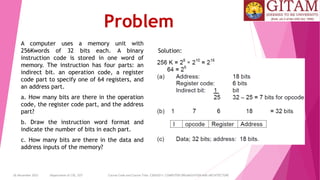
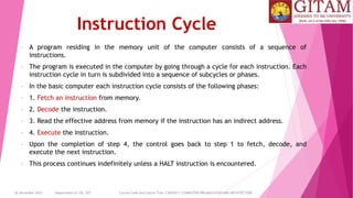
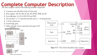
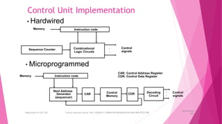
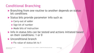
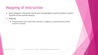
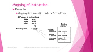
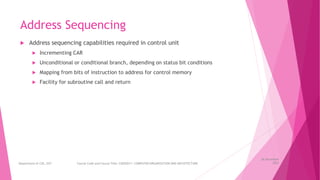
This document discusses the organization and architecture of computers. It covers topics like instruction codes, computer registers, instruction cycles, and memory-referenced instructions. Specifically, it describes:
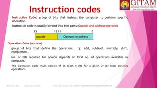
- Instruction codes are made up of operation codes and addresses/operands that instruct the computer to perform operations.
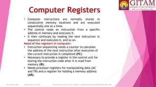
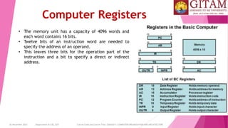
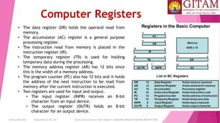
- Computer registers like the program counter, instruction register, and accumulator are needed to process instructions and data.
- The stored program concept allows instructions to be stored in memory and executed sequentially through an instruction cycle.

![26 December 2023 Department of CSE, GST Course Code and Course Title: CSEN2011: COMPUTER ORGANIZATION AND ARCHITECTURE
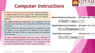
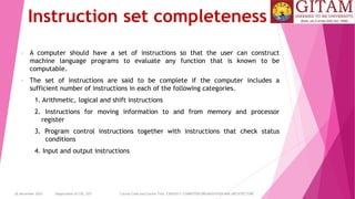
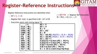
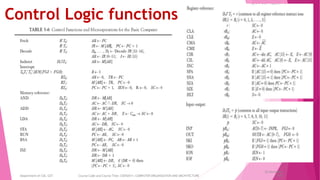
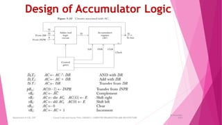
Memory Reference Instructions
AND to AC
D0T4: DR M[AR] Read operand
D0T5: AC AC ^ DR, SC 0 AND with AC
ADD to AC
D1T4: DR M[AR] Read operand
D1T5: AC AC + DR, E Cout, SC 0 Add to AC and store carry in E
LDA: Load to AC
D2T4: DR M[AR]
D2T5: AC DR, SC 0
STA: Store AC
D3T4: M[AR] AC, SC 0
BUN: Branch Unconditionally
D4T4: PC AR, SC 0](https://image.slidesharecdn.com/coamodule2ppt-240219035827-bae63ec9/85/Computer-org-Architecture-module2-ppt-pdf-39-320.jpg)
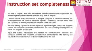
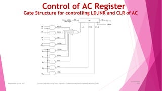
![26 December 2023 Department of CSE, GST Course Code and Course Title: CSEN2011: COMPUTER ORGANIZATION AND ARCHITECTURE
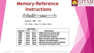
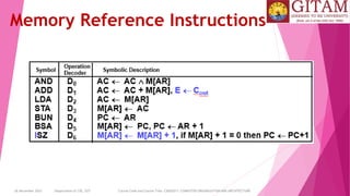
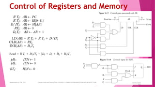
Memory Reference Instructions
BSA: Branch and Save Return Address
D5T4: M[AR] PC, AR AR + 1
D5T5: PC AR, SC 0](https://image.slidesharecdn.com/coamodule2ppt-240219035827-bae63ec9/85/Computer-org-Architecture-module2-ppt-pdf-40-320.jpg)
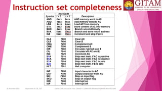
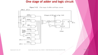
![26 December 2023 Department of CSE, GST Course Code and Course Title: CSEN2011: COMPUTER ORGANIZATION AND ARCHITECTURE
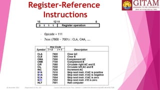
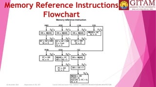
Memory Reference Instructions
ISZ: Increment and Skip-if-Zero
D6T4: DR M[AR]
D6T5: DR DR + 1
D6T4: M[AR] DR, if (DR = 0) then (PC PC + 1), SC 0](https://image.slidesharecdn.com/coamodule2ppt-240219035827-bae63ec9/85/Computer-org-Architecture-module2-ppt-pdf-41-320.jpg)
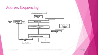
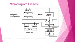
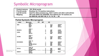
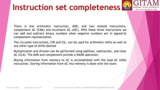
![Microprogram Example
Microinstruction Format
EA is the effective address
Symbol OP-code Description
ADD 0000 AC AC + M[EA]
BRANCH 0001 if (AC < 0) then (PC EA)
STORE 0010 M[EA] AC
EXCHANGE 0011 AC M[EA], M[EA] AC
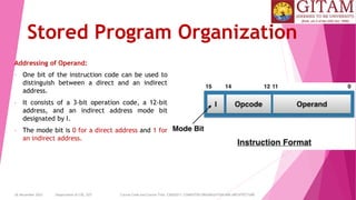
Computer instruction format
I Opcode
15 14 11 10
Address
0
Four computer instructions
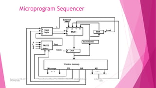
F1 F2 F3 CD BR AD
3 3 3 2 2 7
F1, F2, F3: Microoperation fields
CD: Condition for branching
BR: Branch field
AD: Address field
26 December
2023
Department of CSE, GST Course Code and Course Title: CSEN2011: COMPUTER ORGANIZATION AND ARCHITECTURE](https://image.slidesharecdn.com/coamodule2ppt-240219035827-bae63ec9/85/Computer-org-Architecture-module2-ppt-pdf-74-320.jpg)
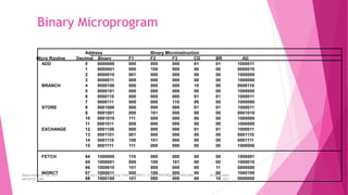
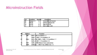
![Microinstruction Fields
F1 Microoperation Symbol
000 None NOP
001 AC AC + DR ADD
010 AC 0 CLRAC
011 AC AC + 1 INCAC
100 AC DR DRTAC
101 AR DR(0-10) DRTAR
110 AR PC PCTAR
111 M[AR] DR WRITE
F2 Microoperation Symbol
000 None NOP
001 AC AC - DR SUB
010 AC AC DR OR
011 AC AC DR AND
100 DR M[AR] READ
101 DR AC ACTDR
110 DR DR + 1 INCDR
111 DR(0-10) PC PCTDR
F3 Microoperation Symbol
000 None NOP
001 AC AC DR XOR
010 AC AC’ COM
011 AC shl AC SHL
100 AC shr AC SHR
101 PC PC + 1 INCPC
110 PC AR ARTPC
111 Reserved
26 December
2023
Department of CSE, GST Course Code and Course Title: CSEN2011: COMPUTER ORGANIZATION AND
ARCHITECTURE](https://image.slidesharecdn.com/coamodule2ppt-240219035827-bae63ec9/85/Computer-org-Architecture-module2-ppt-pdf-75-320.jpg)
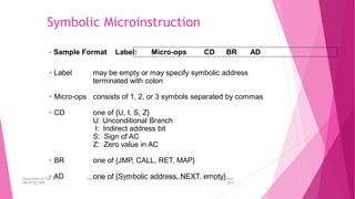
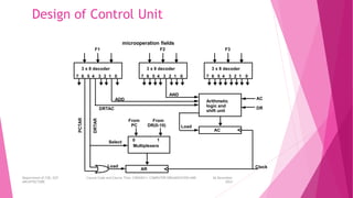
![Fetch Routine
Fetch routine
- Read instruction from memory
- Decode instruction and update PC
AR PC
DR M[AR], PC PC + 1
AR DR(0-10), CAR(2-5) DR(11-14), CAR(0,1,6) 0
Symbolic microprogram for fetch routine:
ORG 64
PCTAR U JMP NEXT
READ, INCPC U JMP NEXT
DRTAR U MAP
FETCH:
Binary microporgram for fetch routine:
1000000 110 000 000 00 00 1000001
1000001 000 100 101 00 00 1000010
1000010 101 000 000 00 11 0000000
Binary
address F1 F2 F3 CD BR AD
Microinstructions for fetch routine:
26 December
2023
Department of CSE, GST Course Code and Course Title: CSEN2011: COMPUTER ORGANIZATION AND
ARCHITECTURE](https://image.slidesharecdn.com/coamodule2ppt-240219035827-bae63ec9/85/Computer-org-Architecture-module2-ppt-pdf-78-320.jpg)