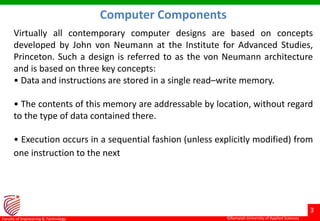
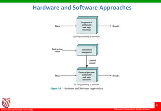
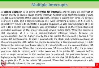
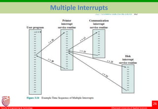
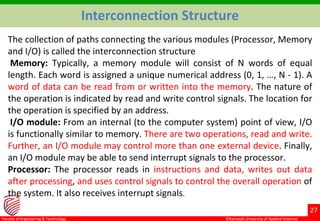
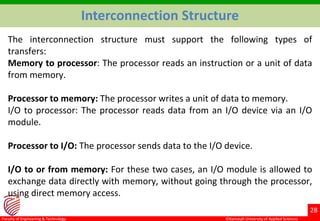
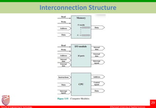
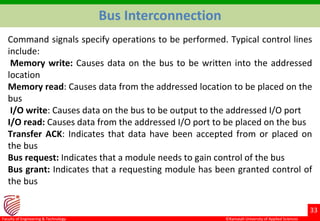
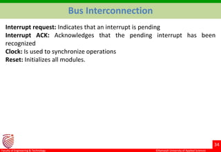
©Ramaiah University of Applied Sciences
1
Faculty of Engineering & Technology ©Ramaiah University of Applied Sciences
1
Faculty of Engineering & Technology
Course Code: 19CSC205A
Course Title: Microprocessor and Assembly
Programming
1
©Ramaiah University of Applied Sciences
2
Faculty of Engineering & Technology ©Ramaiah University of Applied Sciences
2
Faculty of Engineering & Technology
Session-4
Computer Function and Interconnection
2
©Ramaiah University of Applied Sciences
3
Faculty of Engineering & Technology ©Ramaiah University of Applied Sciences
3
Faculty of Engineering & Technology
Computer Components
Virtually all contemporary computer designs are based on concepts
developed by John von Neumann at the Institute for Advanced Studies,
Princeton. Such a design is referred to as the von Neumann architecture
and is based on three key concepts:
• Data and instructions are stored in a single read–write memory.
• The contents of this memory are addressable by location, without regard
to the type of data contained there.
• Execution occurs in a sequential fashion (unless explicitly modified) from
one instruction to the next.
©Ramaiah University of Applied Sciences
4
Faculty of Engineering & Technology ©Ramaiah University of Applied Sciences
4
Faculty of Engineering & Technology
Hardware and Software Approaches
©Ramaiah University of Applied Sciences
5
Faculty of Engineering & Technology ©Ramaiah University of Applied Sciences
5
Faculty of Engineering & Technology
There is a small set of basic logic components that can be combined in
various ways to store binary data and perform arithmetic and logical
operations on that data. If there is a particular computation to be
performed, a configuration of logic components designed specifically for
that computation could be constructed. We can think of the process of
connecting the various components in the desired configuration as a
form of programming. The resulting “program” is in the form of hardware
and is termed a hardwired program.
Suppose we construct a general-purpose configuration of arithmetic and
logic functions. This set of hardware will perform various functions on
data depending on control signals applied to the hardware. In the original
case of customized hardware, the system accepts data and produces
results (Figure 3.1a).
Computer Components
©Ramaiah University of Applied Sciences
6
Faculty of Engineering & Technology ©Ramaiah University of Applied Sciences
6
Faculty of Engineering & Technology
With general-purpose hardware, the system accepts data and control
signals and produces results. Thus, instead of rewiring the hardware for
each new program, the programmer merely needs to supply a new set of
control signals. Programming is now much easier. Instead of rewiring the
hardware for each new program, all we need to do is provide a new
sequence of codes. Each code is, in effect, an instruction, and part of the
hardware interprets each instruction and generates control signals. To
distinguish this new method of programming, a sequence of codes or
instructions is called software.
Figure 3.1b indicates two major components of the system: an instruction
interpreter and a module of general-purpose arithmetic and logic
functions. These two constitute the CPU. Several other components are
needed to yield a functioning computer. Data and instructions must be
put into the system. For this we need some sort of input module. This
module contains basic components for accepting data and instructions in
some form and converting them into an internal form of signals usable by
the system
Computer Components
©Ramaiah University of Applied Sciences
7
Faculty of Engineering & Technology ©Ramaiah University of Applied Sciences
7
Faculty of Engineering & Technology
A means of reporting results is needed, and this is in the form of an output
module. Taken together, these are referred to as I/O components. One more
component is needed. An input device will bring instructions and data in
sequentially. But a program is not invariably executed sequentially; it may
jump around (e.g., the IAS jump instruction). Similarly, operations on data
may require access to more than just one element at a time in a
predetermined sequence. Thus, there must be a place to store temporarily
both instructions and data. That module is called memory, or main memory,
to distinguish it from external storage or peripheral devices. Von Neumann
pointed out that the same memory could be used to store both instructions
and data. data.
Computer Components
©Ramaiah University of Applied Sciences
8
Faculty of Engineering & Technology
Computer Function
Computer Components: Top Level View
©Ramaiah University of Applied Sciences
9
Faculty of Engineering & Technology
Computer Function
The CPU exchanges data with memory. For this purpose, it typically makes
use of two internal (to the CPU) registers:
• A memory address register (MAR), which specifies the address in
memory for the next read or write, and a memory buffer register (MBR),
which contains the data to be written into memory or receives the data
read from memory.
• Similarly, an I/O address register (I/OAR) specifies a particular I/O device.
An I/O buffer (I/OBR) register is used for the exchange of data between
an I/O module and the CPU.
©Ramaiah University of Applied Sciences
10
Faculty of Engineering & Technology
Instruction Fetch and Execute
©Ramaiah University of Applied Sciences
11
Faculty of Engineering & Technology
Instruction Fetch and Execute
• At the beginning of each instruction cycle, the processor fetches an
instruction from memory.
• In a typical processor, a register called the program counter (PC) holds
the address of the instruction to be fetched next
• The fetched instruction is loaded into a register in the processor known
as the instruction register (IR).
• The processor interprets the instruction and performs the required
action. In general, these actions fall into four categories:
Processor-memory: Data may be transferred from processor to memory or
from memory to processor.
Processor-I/O: Data may be transferred to or from a peripheral device by
transferring between the processor and an I/O module.
Data processing: The processor may perform some arithmetic or logic
operation on data.
Control: An instruction may specify that the sequence of execution be
altered.
©Ramaiah University of Applied Sciences
12
Faculty of Engineering & Technology
Instruction Cycle State Diagram
©Ramaiah University of Applied Sciences
13
Faculty of Engineering & Technology
Instruction Cycle State Diagram
• Instruction fetch (if): Read instruction from its memory location into the
processor.
• Instruction operation decoding (iod): Analyze instruction to determine
type of operation to be performed and operand(s) to be used.
• Operand address calculation (oac): If the operation involves reference
to an operand in memory or available via I/O, then determine the
address of the operand.
• Operand fetch (of): Fetch the operand from memory or read it in from
I/O.
• Data operation (do): Perform the operation indicated in the instruction.
• Operand store (os): Write the result into memory or out to I/O.
©Ramaiah University of Applied Sciences
14
Faculty of Engineering & Technology
Classes of Interrupts
©Ramaiah University of Applied Sciences
15
Faculty of Engineering & Technology
Interrupts
Virtually all computers provide a mechanism by which other modules (I/O,
memory) may interrupt the normal processing of the processor
The I/O program consists of three sections:
• A sequence of instructions, labeled 4 in the figure, to prepare for the
actual I/O operation. This may include copying the data to be output into a
special buffer and preparing the parameters for a device command.
• The actual I/O command. Without the use of interrupts, once this
command is issued, the program must wait for the I/O device to perform
the requested function (or periodically poll the device). The program might
wait by simply repeatedly performing a test operation to determine if the
I/O operation is done.
• A sequence of instructions, labeled 5 in the figure, to complete the
operation. This may include setting a flag indicating the success or failure of
the operation.
©Ramaiah University of Applied Sciences
16
Faculty of Engineering & Technology
Interrupts
©Ramaiah University of Applied Sciences
17
Faculty of Engineering & Technology
Interrupts
With interrupts, the processor can be engaged in executing other
instructions while an I/O operation is in progress. Consider the flow of
control in Figure 3.7b. As before, the user program reaches a point at which
it makes a system call in the form of a WRITE call. The I/O program that is
invoked in this case consists only of the preparation code and the actual I/O
command. After these few instructions have been executed, control returns
to the user program. Meanwhile, the external device is busy accepting data
from computer memory and printing it. This I/O operation is conducted
concurrently with the execution of instructions in the user program. When
the external device becomes ready to be serviced—that is, when it is ready
to accept more data from the processor—the I/O module for that external
device sends an interrupt request signal to the processor. The processor
responds by suspending operation of the current program, branching off to
a program to service that particular I/O device, known as an interrupt
handler, and resuming the original execution after the device is serviced.
©Ramaiah University of Applied Sciences
18
Faculty of Engineering & Technology
Interrupts
From the point of view of the
user program, an interrupt is
just that: an interruption of
the normal sequence of
execution. When the interrupt
processing is completed,
execution resumes (Figure
3.8). Thus, the user program
does not have to contain any
special code to accommodate
interrupts; the processor and
the operating system are
responsible for suspending
the user program and then
resuming it at the same point.
©Ramaiah University of Applied Sciences
19
Faculty of Engineering & Technology
Interrupts
To accommodate interrupts, an interrupt cycle is added to the instruction cycle, as shown
in Figure 3.9. In the interrupt cycle, the processor checks to see if any interrupts have
occurred, indicated by the presence of an interrupt signal. If no interrupts are pending,
the processor proceeds to the fetch cycle and fetches the next instruction of the current
program
©Ramaiah University of Applied Sciences
20
Faculty of Engineering & Technology
Interrupts
If an interrupt is pending, the processor does the following:
• It suspends execution of the current program being executed and saves
its context. This means saving the address of the next instruction to be
executed (current contents of the program counter) and any other data
relevant to the processor’s current activity.
• It sets the program counter to the starting address of an interrupt
handler routine.
©Ramaiah University of Applied Sciences
21
Faculty of Engineering & Technology
Multiple Interrupts
Suppose, however, that multiple interrupts can occur. For example, a
program may be receiving data from a communications line and printing
results. The printer will generate an interrupt every time it completes a
print operation. The communication line controller will generate an
interrupt every time a unit of data arrives. The unit could either be a single
character or a block, depending on the nature of the communications
discipline. In any case, it is possible for a communications interrupt to occur
while a printer interrupt is being processed.
©Ramaiah University of Applied Sciences
22
Faculty of Engineering & Technology
Multiple Interrupts
©Ramaiah University of Applied Sciences
23
Faculty of Engineering & Technology
Multiple Interrupts
©Ramaiah University of Applied Sciences
24
Faculty of Engineering & Technology
Multiple Interrupts
Two approaches can be taken to dealing with multiple interrupts.
The first is to disable interrupts while an interrupt is being processed. A
disabled interrupt simply means that the processor can and will ignore that
interrupt request signal. If an interrupt occurs during this time, it generally
remains pending and will be checked by the processor after the processor has
enabled interrupts. Thus, when a user program is executing and an interrupt
occurs, interrupts are disabled immediately. After the interrupt handler
routine completes, interrupts are enabled before resuming the user program,
and the processor checks to see if additional interrupts have occurred. This
approach is nice and simple, as interrupts are handled in strict sequential
order.
The drawback to the preceding approach is that it does not take into account
relative priority or time-critical needs. For example, when input arrives from
the communications line, it may need to be absorbed rapidly to make room for
more input. If the first batch of input has not been processed before the
second batch arrives, data may be lost
©Ramaiah University of Applied Sciences
25
Faculty of Engineering & Technology
Multiple Interrupts
A second approach is to define priorities for interrupts and to allow an interrupt of
higher priority to cause a lower-priority interrupt handler to be itself interrupted (Figure
3.13b). As an example of this second approach, consider a system with three I/O devices:
a printer, a disk, and a communications line, with increasing priorities of 2, 4, and 5,
respectively. Figure 3.14 illustrates a possible sequence. A user program begins at t = 0.
At t = 10, a printer interrupt occurs; user information is placed on the system stack and
execution continues at the printer interrupt service routine (ISR). While this routine is
still executing, at t = 15, a communications interrupt occurs. Because the
communications line has higher priority than the printer, the interrupt is honored. The
printer ISR is interrupted, its state is pushed onto the stack, and execution continues at
the communications ISR. While this routine is executing, a disk interrupt occurs (t = 20).
Because this interrupt is of lower priority, it is simply held, and the communications ISR
runs to completion. When the communications ISR is complete (t = 25), the previous
processor state is restored, which is the execution of the printer ISR. However, before
even a single instruction in that routine can be executed, the processor honors the
higher priority disk interrupt and control transfers to the disk ISR. Only when that routine
is complete (t = 35) is the printer ISR resumed. When that routine completes (t = 40),
control finally returns to the user program
©Ramaiah University of Applied Sciences
26
Faculty of Engineering & Technology
Multiple Interrupts
©Ramaiah University of Applied Sciences
27
Faculty of Engineering & Technology
Interconnection Structure
The collection of paths connecting the various modules (Processor, Memory
and I/O) is called the interconnection structure
Memory: Typically, a memory module will consist of N words of equal
length. Each word is assigned a unique numerical address (0, 1, …, N - 1). A
word of data can be read from or written into the memory. The nature of
the operation is indicated by read and write control signals. The location for
the operation is specified by an address.
I/O module: From an internal (to the computer system) point of view, I/O
is functionally similar to memory. There are two operations, read and write.
Further, an I/O module may control more than one external device. Finally,
an I/O module may be able to send interrupt signals to the processor.
Processor: The processor reads in instructions and data, writes out data
after processing, and uses control signals to control the overall operation of
the system. It also receives interrupt signals.
©Ramaiah University of Applied Sciences
28
Faculty of Engineering & Technology
The interconnection structure must support the following types of
transfers:
Memory to processor: The processor reads an instruction or a unit of data
from memory.
Processor to memory: The processor writes a unit of data to memory.
I/O to processor: The processor reads data from an I/O device via an I/O
module.
Processor to I/O: The processor sends data to the I/O device.
I/O to or from memory: For these two cases, an I/O module is allowed to
exchange data directly with memory, without going through the processor,
using direct memory access.
Interconnection Structure
©Ramaiah University of Applied Sciences
29
Faculty of Engineering & Technology
Interconnection Structure
©Ramaiah University of Applied Sciences
30
Faculty of Engineering & Technology
Bus Interconnection
A bus is a communication pathway connecting two or more devices, it is a
shared transmission medium. Multiple devices connect to the bus, and a
signal transmitted by any one device is available for reception by all other
devices attached to the bus. If two devices transmit during the same time
period, their signals will overlap and become garbled. Thus, only one device
at a time can successfully transmit.
A bus consists of multiple communication pathways or lines. Each line is
capable of transmitting signals representing binary 1 and binary 0. Over
time, a sequence of binary digits can be transmitted across a single line.
Taken together, several lines of a bus can be used to transmit binary digits
simultaneously. For example, an 8-bit unit of data can be transmitted over
eight bus lines. Computer systems contain a number of different buses that
provide pathways between components at various levels of the computer
system hierarchy. A bus that connects major computer components
(processor, memory, I/O) is called a system bus.
©Ramaiah University of Applied Sciences
31
Faculty of Engineering & Technology
Bus Interconnection
©Ramaiah University of Applied Sciences
32
Faculty of Engineering & Technology
• The data lines provide a path for moving data among system modules.
These lines, collectively, are called the data bus.
• The address lines are used to designate the source or destination of the
data on the data bus.
• The control lines are used to control the access to and the use of the
data and address lines. Because the data and address lines are shared by
all components, there must be a means of controlling their use. Control
signals transmit both command and timing information among system
modules. Timing signals indicate the validity of data and address
information.
Bus Interconnection
©Ramaiah University of Applied Sciences
33
Faculty of Engineering & Technology
Command signals specify operations to be performed. Typical control lines
include:
Memory write: Causes data on the bus to be written into the addressed
location
Memory read: Causes data from the addressed location to be placed on the
bus
I/O write: Causes data on the bus to be output to the addressed I/O port
I/O read: Causes data from the addressed I/O port to be placed on the bus
Transfer ACK: Indicates that data have been accepted from or placed on
the bus
Bus request: Indicates that a module needs to gain control of the bus
Bus grant: Indicates that a requesting module has been granted control of
the bus
Bus Interconnection
©Ramaiah University of Applied Sciences
34
Faculty of Engineering & Technology
Interrupt request: Indicates that an interrupt is pending
Interrupt ACK: Acknowledges that the pending interrupt has been
recognized
Clock: Is used to synchronize operations
Reset: Initializes all modules.
Bus Interconnection
©Ramaiah University of Applied Sciences
35
Faculty of Engineering & Technology
PCI Express
The peripheral component interconnect (PCI) is a popular high-bandwidth,
processor independent bus that can function as a mezzanine or peripheral
bus. Compared with other common bus specifications, PCI delivers better
system performance for high speed I/O subsystems (e.g., graphic display
adapters, network interface controllers, and disk controllers).

computer function and interconnection.pptx

  • 1.
    ©Ramaiah University ofApplied Sciences 1 Faculty of Engineering & Technology ©Ramaiah University of Applied Sciences 1 Faculty of Engineering & Technology Course Code: 19CSC205A Course Title: Microprocessor and Assembly Programming 1
  • 2.
    ©Ramaiah University ofApplied Sciences 2 Faculty of Engineering & Technology ©Ramaiah University of Applied Sciences 2 Faculty of Engineering & Technology Session-4 Computer Function and Interconnection 2
  • 3.
    ©Ramaiah University ofApplied Sciences 3 Faculty of Engineering & Technology ©Ramaiah University of Applied Sciences 3 Faculty of Engineering & Technology Computer Components Virtually all contemporary computer designs are based on concepts developed by John von Neumann at the Institute for Advanced Studies, Princeton. Such a design is referred to as the von Neumann architecture and is based on three key concepts: • Data and instructions are stored in a single read–write memory. • The contents of this memory are addressable by location, without regard to the type of data contained there. • Execution occurs in a sequential fashion (unless explicitly modified) from one instruction to the next.
  • 4.
    ©Ramaiah University ofApplied Sciences 4 Faculty of Engineering & Technology ©Ramaiah University of Applied Sciences 4 Faculty of Engineering & Technology Hardware and Software Approaches
  • 5.
    ©Ramaiah University ofApplied Sciences 5 Faculty of Engineering & Technology ©Ramaiah University of Applied Sciences 5 Faculty of Engineering & Technology There is a small set of basic logic components that can be combined in various ways to store binary data and perform arithmetic and logical operations on that data. If there is a particular computation to be performed, a configuration of logic components designed specifically for that computation could be constructed. We can think of the process of connecting the various components in the desired configuration as a form of programming. The resulting “program” is in the form of hardware and is termed a hardwired program. Suppose we construct a general-purpose configuration of arithmetic and logic functions. This set of hardware will perform various functions on data depending on control signals applied to the hardware. In the original case of customized hardware, the system accepts data and produces results (Figure 3.1a). Computer Components
  • 6.
    ©Ramaiah University ofApplied Sciences 6 Faculty of Engineering & Technology ©Ramaiah University of Applied Sciences 6 Faculty of Engineering & Technology With general-purpose hardware, the system accepts data and control signals and produces results. Thus, instead of rewiring the hardware for each new program, the programmer merely needs to supply a new set of control signals. Programming is now much easier. Instead of rewiring the hardware for each new program, all we need to do is provide a new sequence of codes. Each code is, in effect, an instruction, and part of the hardware interprets each instruction and generates control signals. To distinguish this new method of programming, a sequence of codes or instructions is called software. Figure 3.1b indicates two major components of the system: an instruction interpreter and a module of general-purpose arithmetic and logic functions. These two constitute the CPU. Several other components are needed to yield a functioning computer. Data and instructions must be put into the system. For this we need some sort of input module. This module contains basic components for accepting data and instructions in some form and converting them into an internal form of signals usable by the system Computer Components
  • 7.
    ©Ramaiah University ofApplied Sciences 7 Faculty of Engineering & Technology ©Ramaiah University of Applied Sciences 7 Faculty of Engineering & Technology A means of reporting results is needed, and this is in the form of an output module. Taken together, these are referred to as I/O components. One more component is needed. An input device will bring instructions and data in sequentially. But a program is not invariably executed sequentially; it may jump around (e.g., the IAS jump instruction). Similarly, operations on data may require access to more than just one element at a time in a predetermined sequence. Thus, there must be a place to store temporarily both instructions and data. That module is called memory, or main memory, to distinguish it from external storage or peripheral devices. Von Neumann pointed out that the same memory could be used to store both instructions and data. data. Computer Components
  • 8.
    ©Ramaiah University ofApplied Sciences 8 Faculty of Engineering & Technology Computer Function Computer Components: Top Level View
  • 9.
    ©Ramaiah University ofApplied Sciences 9 Faculty of Engineering & Technology Computer Function The CPU exchanges data with memory. For this purpose, it typically makes use of two internal (to the CPU) registers: • A memory address register (MAR), which specifies the address in memory for the next read or write, and a memory buffer register (MBR), which contains the data to be written into memory or receives the data read from memory. • Similarly, an I/O address register (I/OAR) specifies a particular I/O device. An I/O buffer (I/OBR) register is used for the exchange of data between an I/O module and the CPU.
  • 10.
    ©Ramaiah University ofApplied Sciences 10 Faculty of Engineering & Technology Instruction Fetch and Execute
  • 11.
    ©Ramaiah University ofApplied Sciences 11 Faculty of Engineering & Technology Instruction Fetch and Execute • At the beginning of each instruction cycle, the processor fetches an instruction from memory. • In a typical processor, a register called the program counter (PC) holds the address of the instruction to be fetched next • The fetched instruction is loaded into a register in the processor known as the instruction register (IR). • The processor interprets the instruction and performs the required action. In general, these actions fall into four categories: Processor-memory: Data may be transferred from processor to memory or from memory to processor. Processor-I/O: Data may be transferred to or from a peripheral device by transferring between the processor and an I/O module. Data processing: The processor may perform some arithmetic or logic operation on data. Control: An instruction may specify that the sequence of execution be altered.
  • 12.
    ©Ramaiah University ofApplied Sciences 12 Faculty of Engineering & Technology Instruction Cycle State Diagram
  • 13.
    ©Ramaiah University ofApplied Sciences 13 Faculty of Engineering & Technology Instruction Cycle State Diagram • Instruction fetch (if): Read instruction from its memory location into the processor. • Instruction operation decoding (iod): Analyze instruction to determine type of operation to be performed and operand(s) to be used. • Operand address calculation (oac): If the operation involves reference to an operand in memory or available via I/O, then determine the address of the operand. • Operand fetch (of): Fetch the operand from memory or read it in from I/O. • Data operation (do): Perform the operation indicated in the instruction. • Operand store (os): Write the result into memory or out to I/O.
  • 14.
    ©Ramaiah University ofApplied Sciences 14 Faculty of Engineering & Technology Classes of Interrupts
  • 15.
    ©Ramaiah University ofApplied Sciences 15 Faculty of Engineering & Technology Interrupts Virtually all computers provide a mechanism by which other modules (I/O, memory) may interrupt the normal processing of the processor The I/O program consists of three sections: • A sequence of instructions, labeled 4 in the figure, to prepare for the actual I/O operation. This may include copying the data to be output into a special buffer and preparing the parameters for a device command. • The actual I/O command. Without the use of interrupts, once this command is issued, the program must wait for the I/O device to perform the requested function (or periodically poll the device). The program might wait by simply repeatedly performing a test operation to determine if the I/O operation is done. • A sequence of instructions, labeled 5 in the figure, to complete the operation. This may include setting a flag indicating the success or failure of the operation.
  • 16.
    ©Ramaiah University ofApplied Sciences 16 Faculty of Engineering & Technology Interrupts
  • 17.
    ©Ramaiah University ofApplied Sciences 17 Faculty of Engineering & Technology Interrupts With interrupts, the processor can be engaged in executing other instructions while an I/O operation is in progress. Consider the flow of control in Figure 3.7b. As before, the user program reaches a point at which it makes a system call in the form of a WRITE call. The I/O program that is invoked in this case consists only of the preparation code and the actual I/O command. After these few instructions have been executed, control returns to the user program. Meanwhile, the external device is busy accepting data from computer memory and printing it. This I/O operation is conducted concurrently with the execution of instructions in the user program. When the external device becomes ready to be serviced—that is, when it is ready to accept more data from the processor—the I/O module for that external device sends an interrupt request signal to the processor. The processor responds by suspending operation of the current program, branching off to a program to service that particular I/O device, known as an interrupt handler, and resuming the original execution after the device is serviced.
  • 18.
    ©Ramaiah University ofApplied Sciences 18 Faculty of Engineering & Technology Interrupts From the point of view of the user program, an interrupt is just that: an interruption of the normal sequence of execution. When the interrupt processing is completed, execution resumes (Figure 3.8). Thus, the user program does not have to contain any special code to accommodate interrupts; the processor and the operating system are responsible for suspending the user program and then resuming it at the same point.
  • 19.
    ©Ramaiah University ofApplied Sciences 19 Faculty of Engineering & Technology Interrupts To accommodate interrupts, an interrupt cycle is added to the instruction cycle, as shown in Figure 3.9. In the interrupt cycle, the processor checks to see if any interrupts have occurred, indicated by the presence of an interrupt signal. If no interrupts are pending, the processor proceeds to the fetch cycle and fetches the next instruction of the current program
  • 20.
    ©Ramaiah University ofApplied Sciences 20 Faculty of Engineering & Technology Interrupts If an interrupt is pending, the processor does the following: • It suspends execution of the current program being executed and saves its context. This means saving the address of the next instruction to be executed (current contents of the program counter) and any other data relevant to the processor’s current activity. • It sets the program counter to the starting address of an interrupt handler routine.
  • 21.
    ©Ramaiah University ofApplied Sciences 21 Faculty of Engineering & Technology Multiple Interrupts Suppose, however, that multiple interrupts can occur. For example, a program may be receiving data from a communications line and printing results. The printer will generate an interrupt every time it completes a print operation. The communication line controller will generate an interrupt every time a unit of data arrives. The unit could either be a single character or a block, depending on the nature of the communications discipline. In any case, it is possible for a communications interrupt to occur while a printer interrupt is being processed.
  • 22.
    ©Ramaiah University ofApplied Sciences 22 Faculty of Engineering & Technology Multiple Interrupts
  • 23.
    ©Ramaiah University ofApplied Sciences 23 Faculty of Engineering & Technology Multiple Interrupts
  • 24.
    ©Ramaiah University ofApplied Sciences 24 Faculty of Engineering & Technology Multiple Interrupts Two approaches can be taken to dealing with multiple interrupts. The first is to disable interrupts while an interrupt is being processed. A disabled interrupt simply means that the processor can and will ignore that interrupt request signal. If an interrupt occurs during this time, it generally remains pending and will be checked by the processor after the processor has enabled interrupts. Thus, when a user program is executing and an interrupt occurs, interrupts are disabled immediately. After the interrupt handler routine completes, interrupts are enabled before resuming the user program, and the processor checks to see if additional interrupts have occurred. This approach is nice and simple, as interrupts are handled in strict sequential order. The drawback to the preceding approach is that it does not take into account relative priority or time-critical needs. For example, when input arrives from the communications line, it may need to be absorbed rapidly to make room for more input. If the first batch of input has not been processed before the second batch arrives, data may be lost
  • 25.
    ©Ramaiah University ofApplied Sciences 25 Faculty of Engineering & Technology Multiple Interrupts A second approach is to define priorities for interrupts and to allow an interrupt of higher priority to cause a lower-priority interrupt handler to be itself interrupted (Figure 3.13b). As an example of this second approach, consider a system with three I/O devices: a printer, a disk, and a communications line, with increasing priorities of 2, 4, and 5, respectively. Figure 3.14 illustrates a possible sequence. A user program begins at t = 0. At t = 10, a printer interrupt occurs; user information is placed on the system stack and execution continues at the printer interrupt service routine (ISR). While this routine is still executing, at t = 15, a communications interrupt occurs. Because the communications line has higher priority than the printer, the interrupt is honored. The printer ISR is interrupted, its state is pushed onto the stack, and execution continues at the communications ISR. While this routine is executing, a disk interrupt occurs (t = 20). Because this interrupt is of lower priority, it is simply held, and the communications ISR runs to completion. When the communications ISR is complete (t = 25), the previous processor state is restored, which is the execution of the printer ISR. However, before even a single instruction in that routine can be executed, the processor honors the higher priority disk interrupt and control transfers to the disk ISR. Only when that routine is complete (t = 35) is the printer ISR resumed. When that routine completes (t = 40), control finally returns to the user program
  • 26.
    ©Ramaiah University ofApplied Sciences 26 Faculty of Engineering & Technology Multiple Interrupts
  • 27.
    ©Ramaiah University ofApplied Sciences 27 Faculty of Engineering & Technology Interconnection Structure The collection of paths connecting the various modules (Processor, Memory and I/O) is called the interconnection structure Memory: Typically, a memory module will consist of N words of equal length. Each word is assigned a unique numerical address (0, 1, …, N - 1). A word of data can be read from or written into the memory. The nature of the operation is indicated by read and write control signals. The location for the operation is specified by an address. I/O module: From an internal (to the computer system) point of view, I/O is functionally similar to memory. There are two operations, read and write. Further, an I/O module may control more than one external device. Finally, an I/O module may be able to send interrupt signals to the processor. Processor: The processor reads in instructions and data, writes out data after processing, and uses control signals to control the overall operation of the system. It also receives interrupt signals.
  • 28.
    ©Ramaiah University ofApplied Sciences 28 Faculty of Engineering & Technology The interconnection structure must support the following types of transfers: Memory to processor: The processor reads an instruction or a unit of data from memory. Processor to memory: The processor writes a unit of data to memory. I/O to processor: The processor reads data from an I/O device via an I/O module. Processor to I/O: The processor sends data to the I/O device. I/O to or from memory: For these two cases, an I/O module is allowed to exchange data directly with memory, without going through the processor, using direct memory access. Interconnection Structure
  • 29.
    ©Ramaiah University ofApplied Sciences 29 Faculty of Engineering & Technology Interconnection Structure
  • 30.
    ©Ramaiah University ofApplied Sciences 30 Faculty of Engineering & Technology Bus Interconnection A bus is a communication pathway connecting two or more devices, it is a shared transmission medium. Multiple devices connect to the bus, and a signal transmitted by any one device is available for reception by all other devices attached to the bus. If two devices transmit during the same time period, their signals will overlap and become garbled. Thus, only one device at a time can successfully transmit. A bus consists of multiple communication pathways or lines. Each line is capable of transmitting signals representing binary 1 and binary 0. Over time, a sequence of binary digits can be transmitted across a single line. Taken together, several lines of a bus can be used to transmit binary digits simultaneously. For example, an 8-bit unit of data can be transmitted over eight bus lines. Computer systems contain a number of different buses that provide pathways between components at various levels of the computer system hierarchy. A bus that connects major computer components (processor, memory, I/O) is called a system bus.
  • 31.
    ©Ramaiah University ofApplied Sciences 31 Faculty of Engineering & Technology Bus Interconnection
  • 32.
    ©Ramaiah University ofApplied Sciences 32 Faculty of Engineering & Technology • The data lines provide a path for moving data among system modules. These lines, collectively, are called the data bus. • The address lines are used to designate the source or destination of the data on the data bus. • The control lines are used to control the access to and the use of the data and address lines. Because the data and address lines are shared by all components, there must be a means of controlling their use. Control signals transmit both command and timing information among system modules. Timing signals indicate the validity of data and address information. Bus Interconnection
  • 33.
    ©Ramaiah University ofApplied Sciences 33 Faculty of Engineering & Technology Command signals specify operations to be performed. Typical control lines include: Memory write: Causes data on the bus to be written into the addressed location Memory read: Causes data from the addressed location to be placed on the bus I/O write: Causes data on the bus to be output to the addressed I/O port I/O read: Causes data from the addressed I/O port to be placed on the bus Transfer ACK: Indicates that data have been accepted from or placed on the bus Bus request: Indicates that a module needs to gain control of the bus Bus grant: Indicates that a requesting module has been granted control of the bus Bus Interconnection
  • 34.
    ©Ramaiah University ofApplied Sciences 34 Faculty of Engineering & Technology Interrupt request: Indicates that an interrupt is pending Interrupt ACK: Acknowledges that the pending interrupt has been recognized Clock: Is used to synchronize operations Reset: Initializes all modules. Bus Interconnection
  • 35.
    ©Ramaiah University ofApplied Sciences 35 Faculty of Engineering & Technology PCI Express The peripheral component interconnect (PCI) is a popular high-bandwidth, processor independent bus that can function as a mezzanine or peripheral bus. Compared with other common bus specifications, PCI delivers better system performance for high speed I/O subsystems (e.g., graphic display adapters, network interface controllers, and disk controllers).