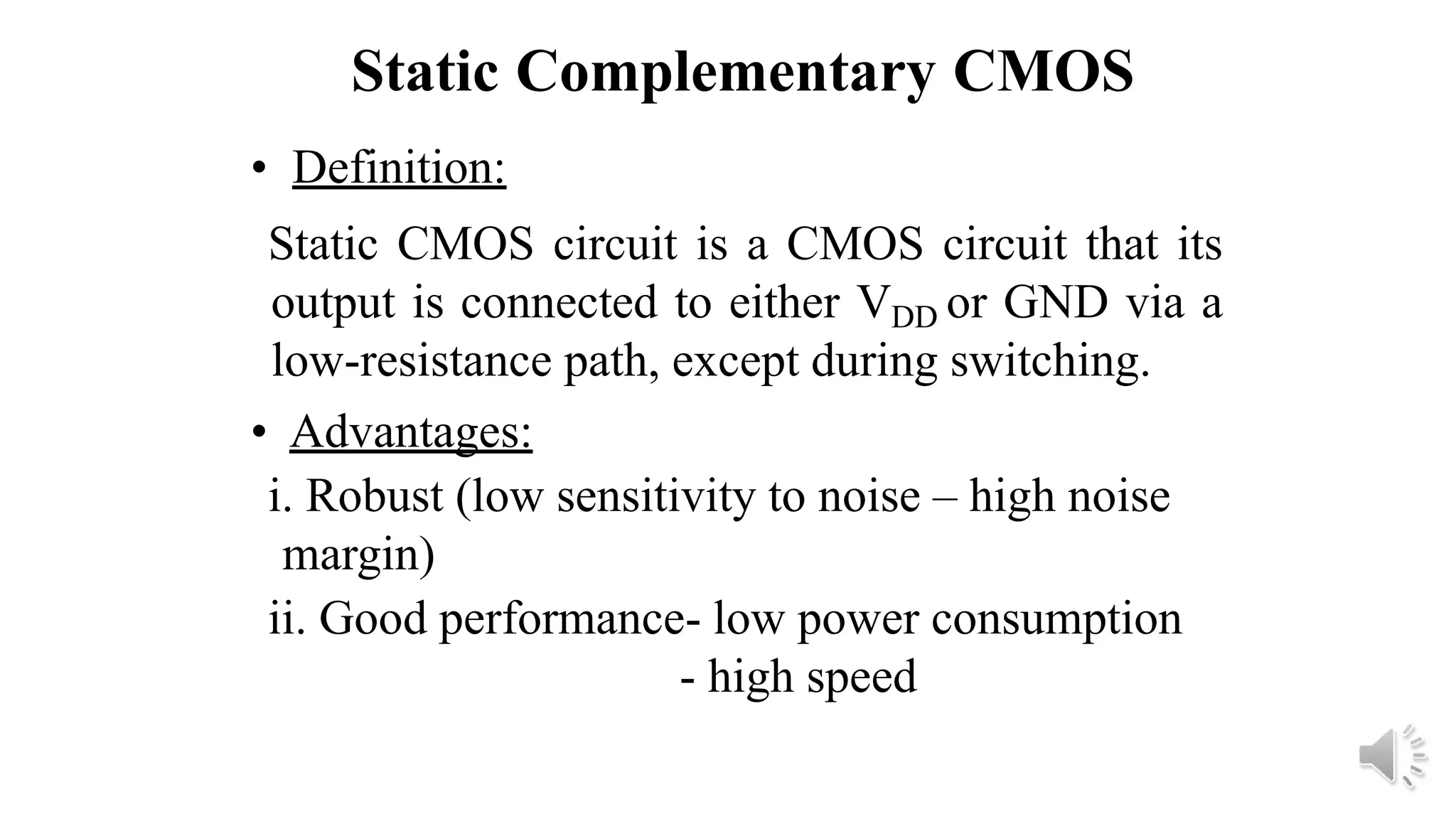
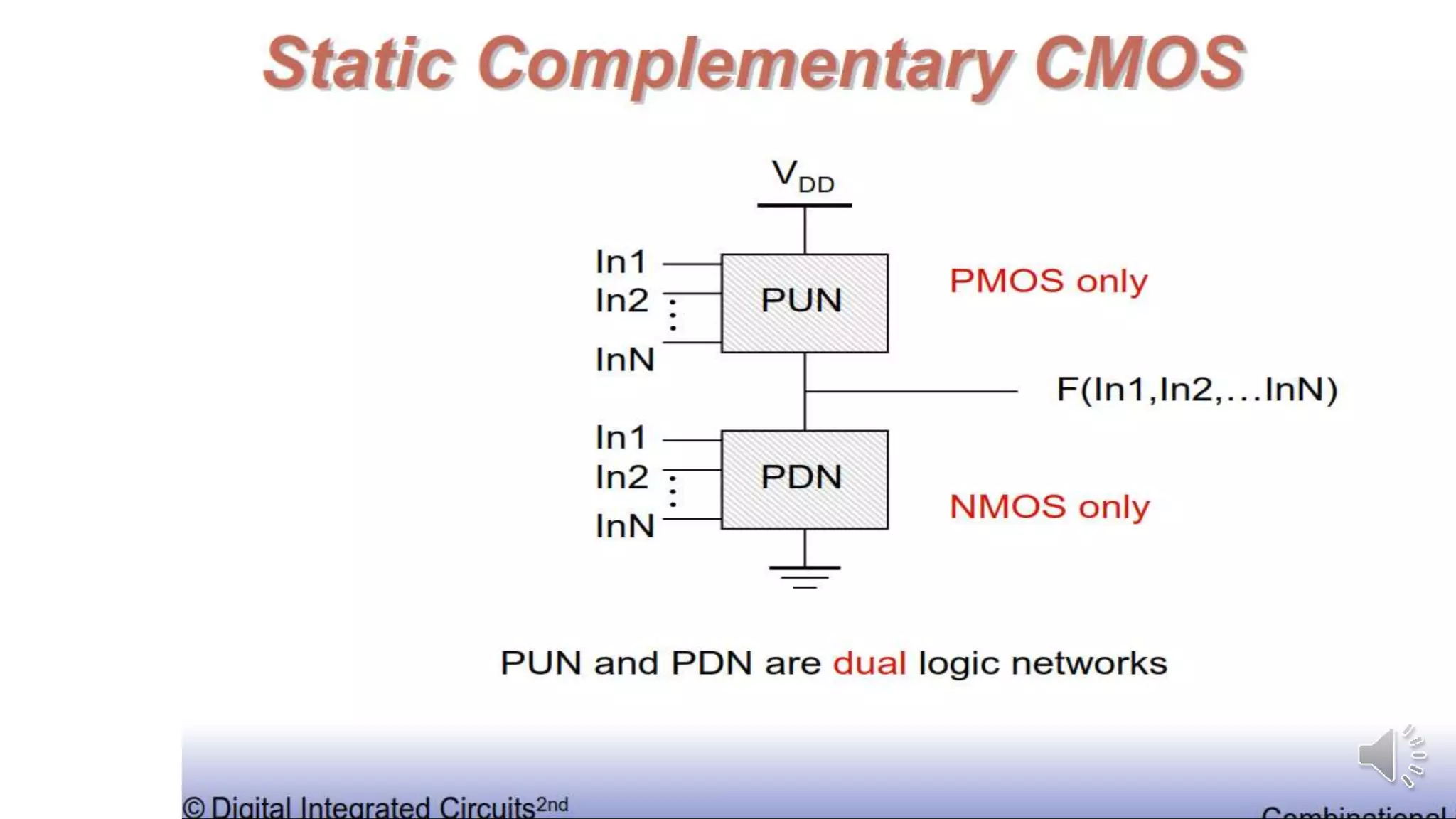
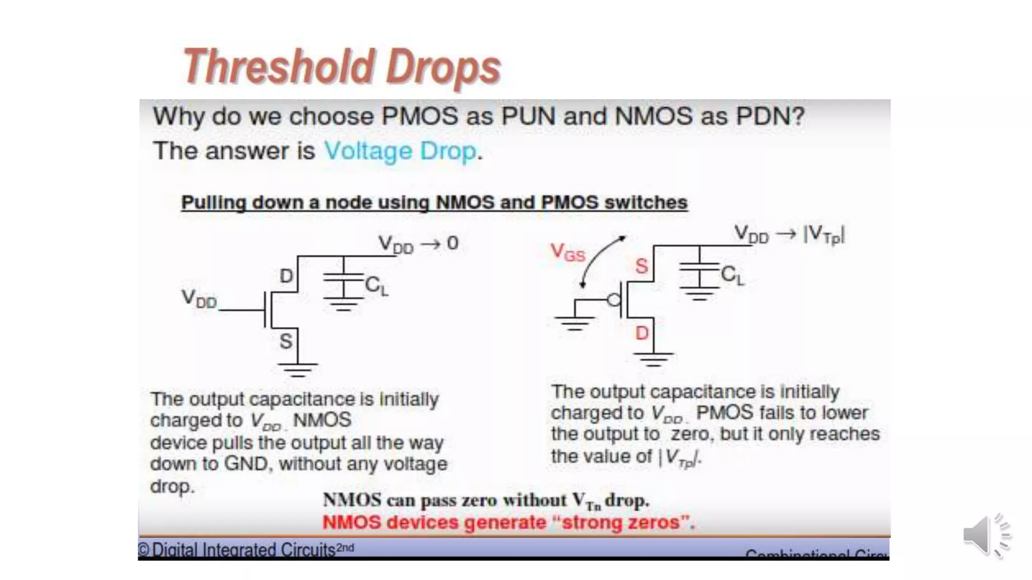
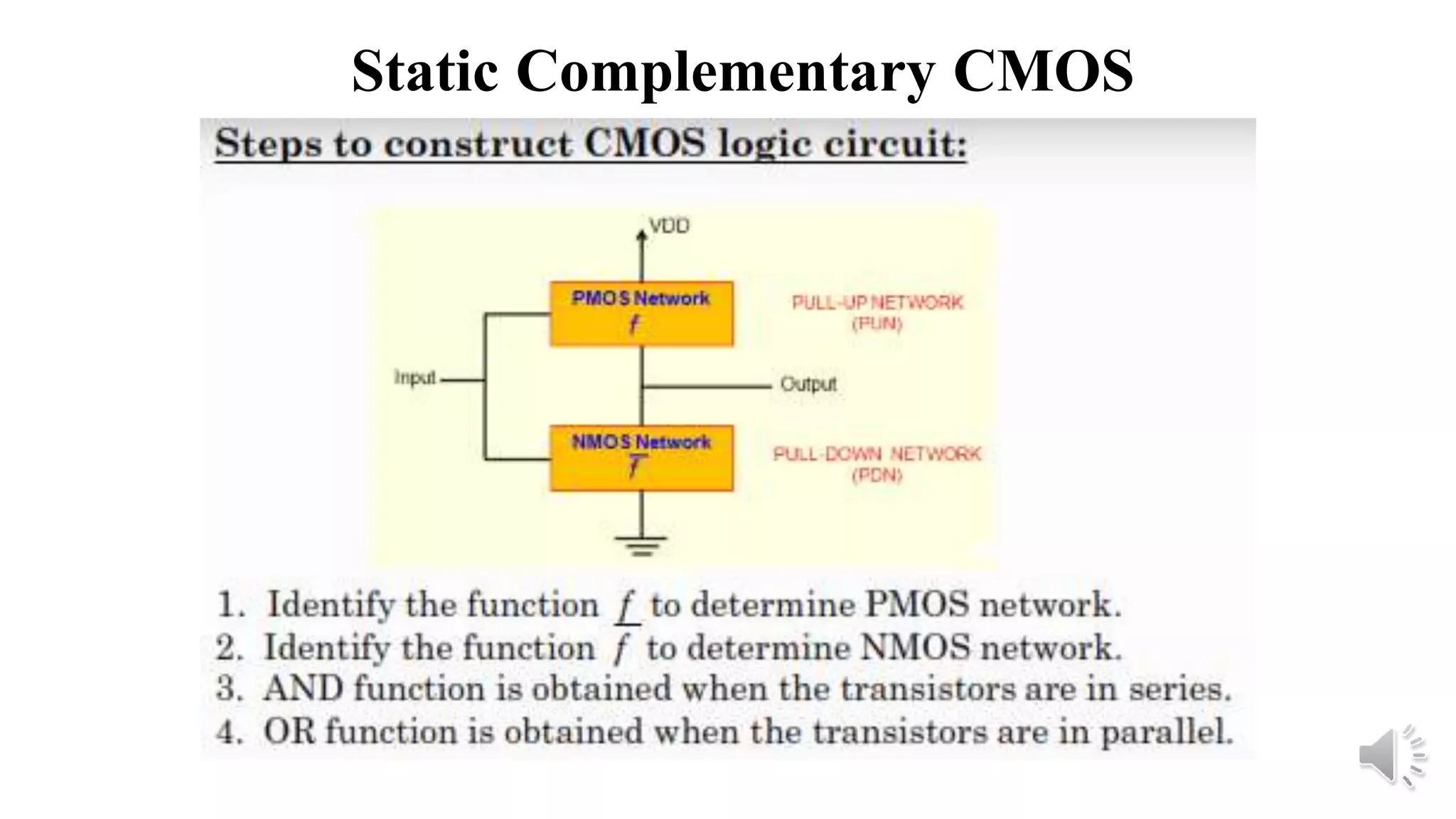
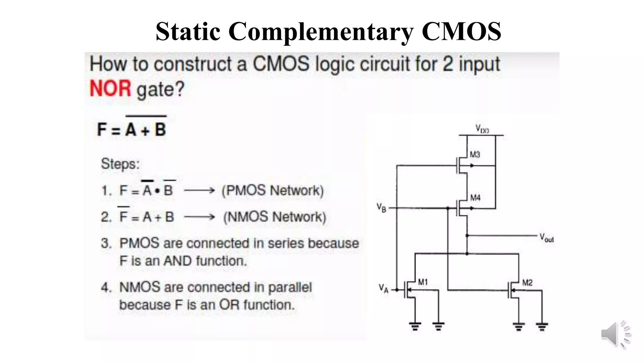
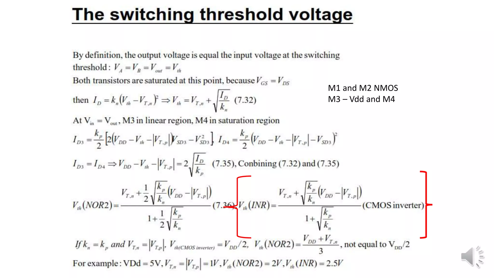
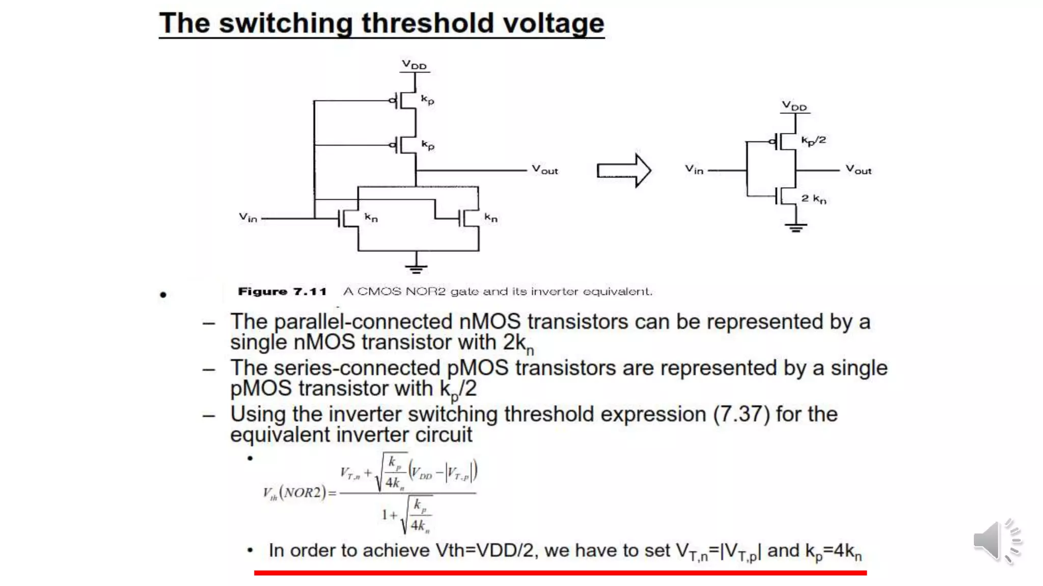
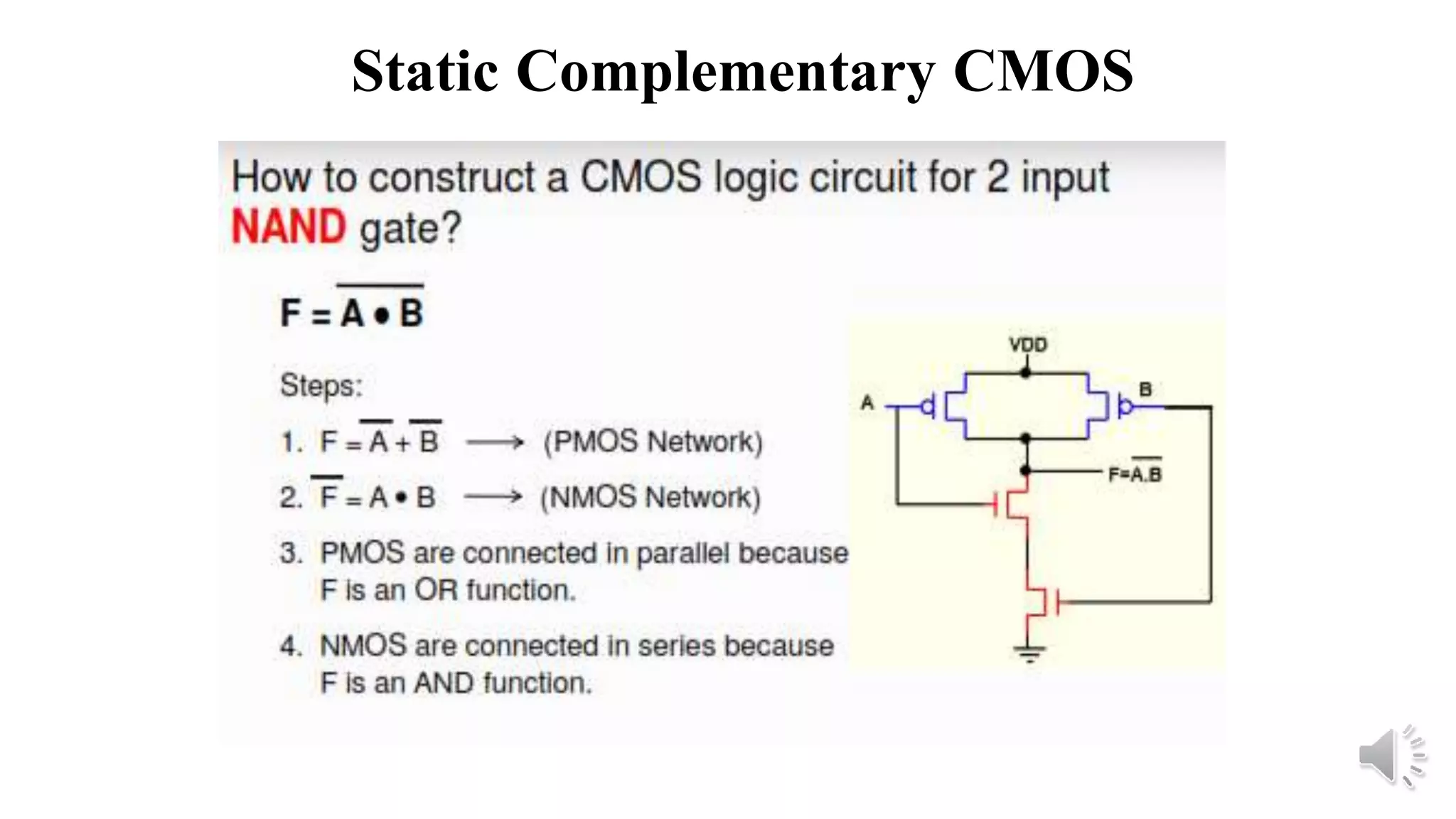
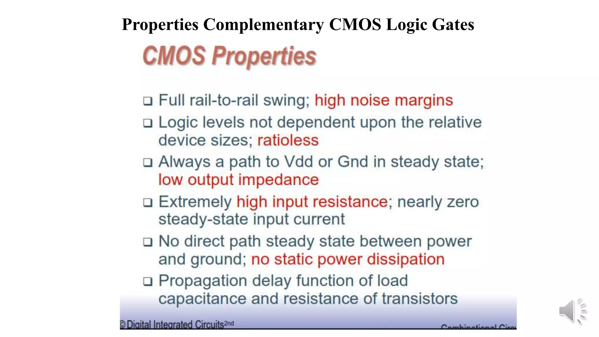
Static complementary CMOS logic circuits have the following properties:
1) They are robust and have high noise immunity since their output is connected to either VDD or GND through a low-resistance path except during switching.
2) They have low power consumption and high speed.
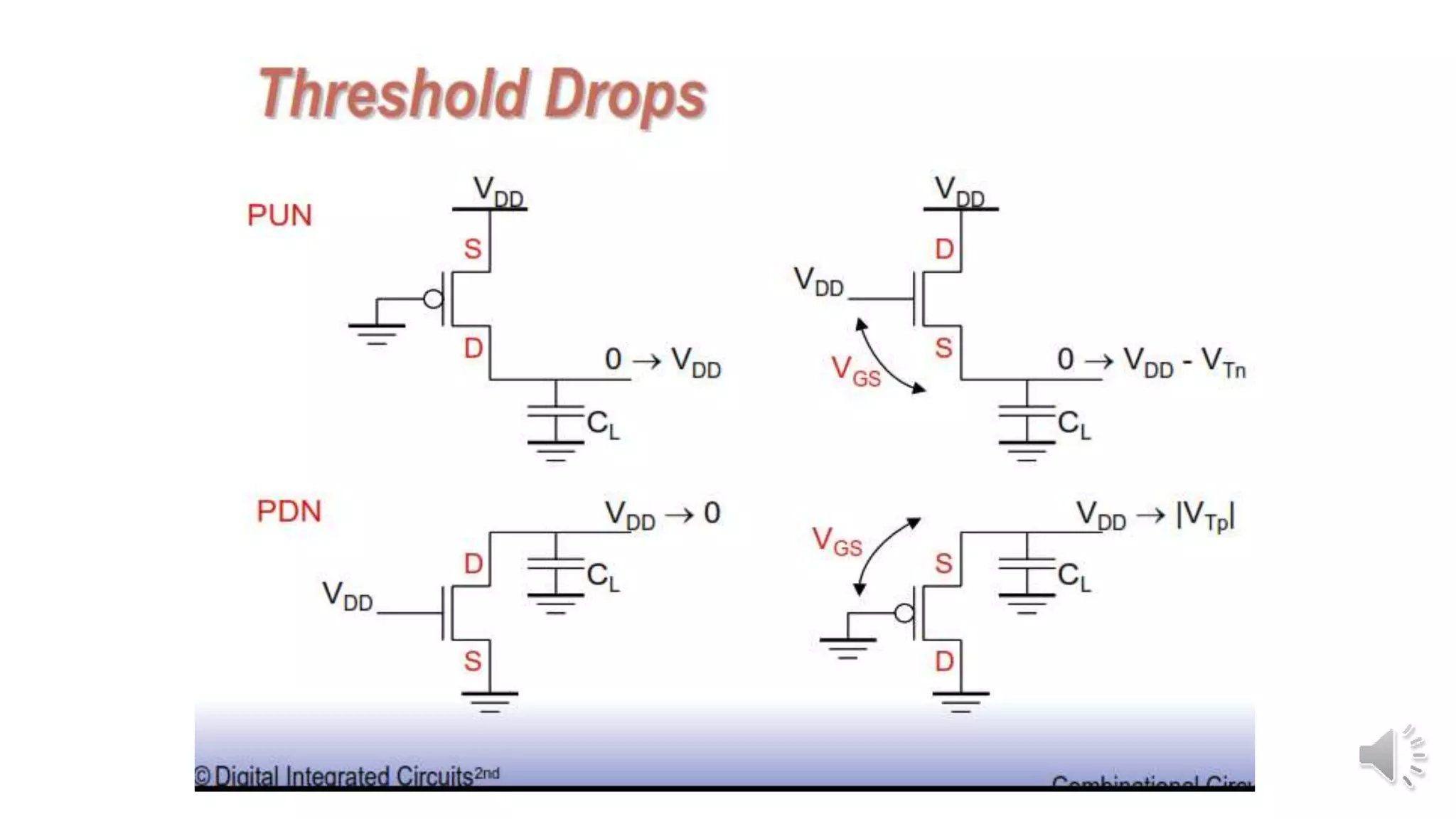
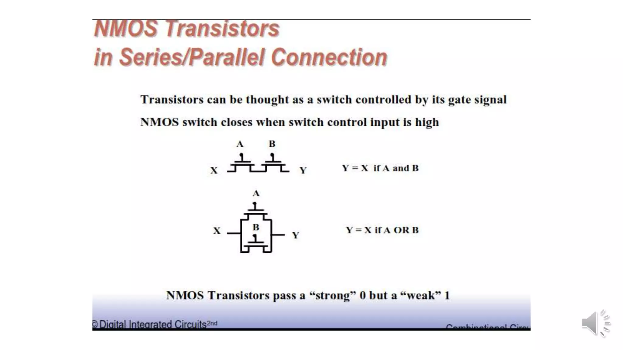
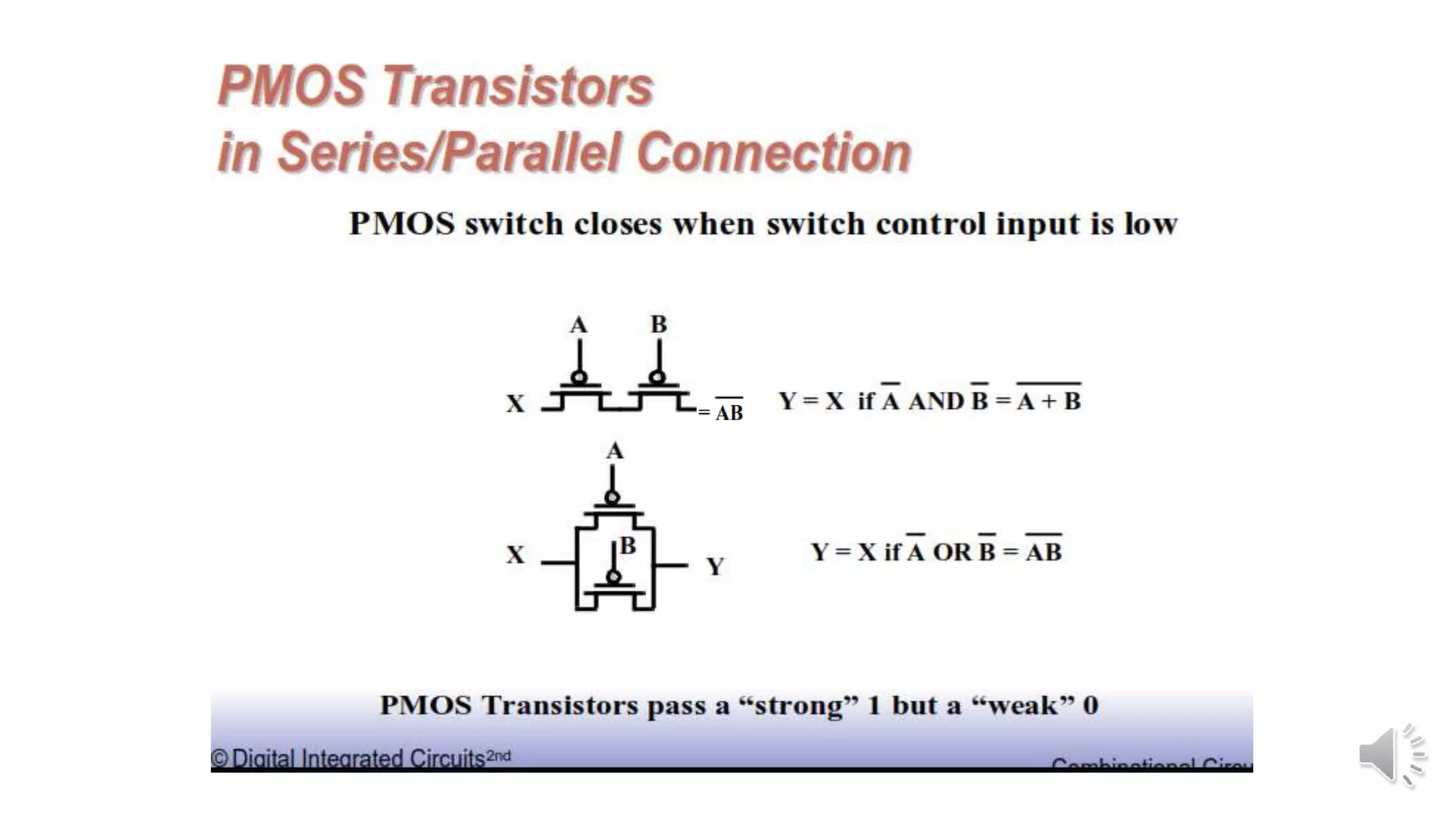
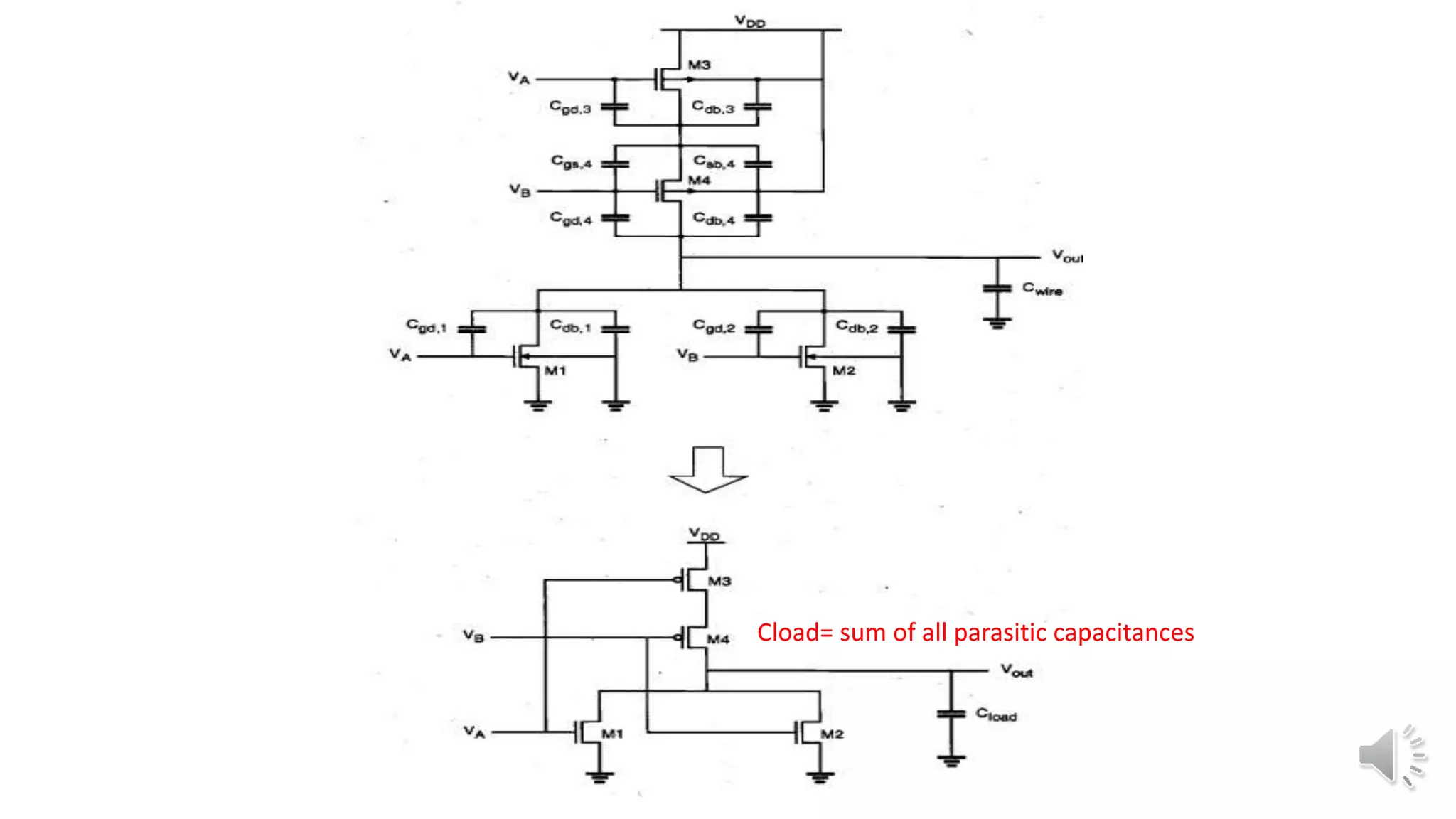
3) They use both NMOS and PMOS transistors - the NMOS transistors (M1 and M2) pull the output low, while the PMOS transistors (M3 and M4) pull the output high. The load is the total parasitic capacitance (Cload).