Characterizing the Heterogeneity of 2D Materials with Transmission Electron Microscopy and Machine Learning

2023/03/31 Chia-Hao Lee's PhD Defense @ UIUC Supercon 2008 Advisor: Prof. Pinshane Huang Committee: Prof. Pinshane Huang, Prof. Jian-Min Zuo, Prof. Andre Schleife, Prof. Vidya Madhavan Youtube recording: https://youtu.be/oJhY6ZOJabo Personal website: https://sites.google.com/view/chiahao-lee Research Summary: My research explores the use of advanced microscopy techniques and machine learning algorithms to understand the heterogeneities of two-dimensional (2D) materials. While 2D materials exhibit a wide range of unique properties that make them ideal candidates for various applications, including flexible electronics, energy conversion, and catalysis, their properties can vary significantly due to their heterogeneity, which arises from the presence of defects, grain boundaries, and other structural imperfections. I combined the class-averaging technique with deep learning models for defect identification to generate high signal-to-noise images of single-atom defects. These images provide the 1st direct observation of oscillating strain fields around a single atom vacancy with sub-pm precision. Additionally, I co-developed an AI-in-the-loop framework that combines a cycle generative adversarial network with automatic acquisition and image simulation. This framework generates high quality training data that greatly enhances the generalizability of machine learning applications. Furthermore, I explored the anisotropic phase transition kinetics of few-layer MoTe2, a promising phase-change material, using in situ heating, dark-field TEM, and aberration-corrected STEM. Most recently, I applied electron ptychography on 2D materials and obtained unprecedented details about their local lattice distortion and rippling with 0.4 Å resolution, greatly surpassing the conventional approaches. In summary, my research demonstrates a combination of new S/TEM techniques with machine learning, enabling atom-by-atom characterization of heterogeneities of 2D materials including phase boundaries, strain, point defects, and local rippling with high precision. Overall, these techniques pave the way for the development of reliable and efficient 2D electronics, making significant contributions to the field of nanotechnology.

Recommended
Recommended
More Related Content
Similar to Characterizing the Heterogeneity of 2D Materials with Transmission Electron Microscopy and Machine Learning
Similar to Characterizing the Heterogeneity of 2D Materials with Transmission Electron Microscopy and Machine Learning (20)
Recently uploaded
Recently uploaded (20)
Characterizing the Heterogeneity of 2D Materials with Transmission Electron Microscopy and Machine Learning
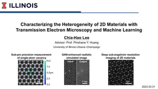
- 1. Characterizing the Heterogeneity of 2D Materials with Transmission Electron Microscopy and Machine Learning Chia-Hao Lee Advisor: Prof. Pinshane Y. Huang University of Illinois Urbana–Champaign 2023.03.31 GAN-enhanced realistic simulated image 1 nm Input Output Deep sub-angstrom resolution imaging of 2D materials Sub-pm precision measurement of single-atom vacancy 5 Å pm 10.0 0.0 - - - 5.0 - - 7.5 2.5 5 Å
- 2. Acknowledgments Dr. Di Luo Prof. Bryan K. Clark Abid Khan Chuqiao Shi Prof. Arend van der Zande Dr. M. Abir Hossain Prof. Pinshane Y. Huang Main Collaborators Yue Zhang FA9550-17-1-0213 DE-SC0020190 Huang Group 2 / 38
- 3. Why 2D materials? 1. 2D confinement-induced physical properties 2. High tunability of properties via defects and strain 3. Flexible heterostructures design In WSe2, 0.4% tensile strain can enhance the e- mobility by 84% 3 / 38 Geim, A. K. (2013), Nature Because they’re atomically thin…… Atom-by-atom characterization routinely achieved with aberration corrected STEM WSe2-2xTe2x Annular Dark-Field STEM image 5 nm
- 4. STEM as an atomic-scale characterization tool 4 / 38 Electron - Sample Interactions Z+ Annular Detector Low angle scattering Inelastic scattering High angle scattering, Annular dark-field (ADF) θ Strong Z dependence as Rutherford scattering Scanning Transmission Electron Microscopy (STEM) Electron gun Electromagnetic lens system Sample Annular Detector Spectrometer Fine e- probe ~1Å e- transparent
- 5. Understanding heterogeneities of 2D materials at atomic scale Sub-pm precision measurement of single-atom vacancy 5 Å pm 10.0 0.0 - - - 5.0 - - 7.5 2.5 Lee, C.-H., et al. (2020). Nano Letters, 20(5), 3369-3377. What are the precise structures of single-atom defect? GAN-enhanced realistic simulated images for ML 1 nm Input Output Khan, A., Lee, C.-H., et al. (Under Review) arXiv: 2301.07743 How to get defect types and densities at larger scale? Deep sub-angstrom resolution imaging of 2D materials Lee, C.-H., et al. (In preparation) How does 2D materials look like at deep sub-Å level? 5 Å 5 / 38
- 6. Defect-induced strain fields in 2D materials 1D Vacancy Line Wang, S., et al. (2016) ACS nano 5-7-5-7 to 6-6-6-6 Ring Exchange Huang, P. Y., et al. (2013) Science Azizi, A., et al. (2017) Nano Letters Vacancy and Substitutional defect However, the measurement precision is still around 8-20 pm, limiting the strain analyses to 2.5% or more. 6 / 38 For WSe2, 1% tensile strain can change the exciton energy by 50 meV.
- 7. Challenges in probing the atomic defects ADF-STEM, 80kV, 35pA, dwell 4μs, 15.3 nm x 15.3 nm, 120 frames 5 nm WSe2-2xTe2x Single frame dose: 3.9x10⁶ e-/nm2 Total dose: 4.7x10⁸ e-/nm2 Radiation damage is the limiting factor of achievable SNR, hence the precision in 2D materials Challenges 1. Spatial resolution 2. Low signal intensity 3. Detection limit 4. Defect Identification 5. Beam sensitivity 7 / 38
- 8. Our approach: Class averaging with FCN deep learning Class averaging (Rigid-registration) 4. Class-averaged image SeTe 3 Å 8 / 38 High SNR image is obtained by class-averaging “equivalent defect sites” identified by deep learning. Lee, C.-H., et al. (2020). Nano Letters, 20(5), 3369-3377 1. ADF-STEM image WSe2-2xTe2x 2 nm • 80kV, aberration-corrected • α = 25 mrad, probe size 95 pm • 10-frame averaged, frame time 3 s • Dwell 2 μs, total dose 107 e-/nm2 2. Identified defect sites • Fully Convolutional Network (FCN) • 4 networks for different chalcogen defects • Trained on simulated STEM images • Recall, precision, and F1 score all >99% • • • • 2Te SeTe Single Vacancy (Se) Double Vacancy Section “isolated” defects Deep Learning W 2Se SeTe W 2Se SeTe 2 equivalent chalcogen sites! 3. Defect images SeTe sites
- 9. How does a single Te “squeeze” into WSe2 lattice? 2D Gaussian fitting 2D Gaussian fitting Sum of 437 Defect-free sites 2Se Sum of 312 Substitution SeTe sites SeTe Defect-free 2Se sites Substitution SeTe sites 3 Å Raw Precision = 0.3 pm Class-averaged 2.1 pm Precision = 5.9 pm 9 / 38 W-W W-W W-W W-W
- 10. How SNR and precision scale with number of images? 10 / 38 1 10 100 50 200 SNR = μ𝑠𝑖𝑔𝑛𝑎𝑙 σ𝑛𝑜𝑖𝑠𝑒 SNR Gain = 𝑆𝑁𝑅𝑠𝑢𝑚𝑚𝑒𝑑 𝑆𝑁𝑅𝑟𝑎𝑤 Precision = σ(𝐴𝑙𝑙 𝑎𝑣𝑔 𝑊 − 𝑊) 3 Å Images summed with different number of frames (N) The SNR gain is proportional to 𝑵 and allows high precision measurement after class averaging. SNR determines the precision until the instrument stability becomes the limiting factor. ∝ ~ 𝑁 ∝ ~ 𝑃𝑖𝑛𝑖𝑡𝑖𝑎𝑙 𝑁 Precision and SNR gain Precision ~ 0.27 pm → Still limited by number of frames!
- 11. How different defects distort the lattice? Class-averaged DV SeTe 2Se 2Te SV Expansion Contraction We measured local distortions of multiple defect types and observed strong contraction around vacancies. 11 / 38 5 Å 1st NN 5 Å 10 0 - - - 5.0 pm - - 7.5 2.5 SV Displacement vectors map Vectors are enlarged 18x for visibility.
- 12. 2939 εxx εyy Dilation (εxx+ εyy) Exp x y 5 Å Precision: 0.2 pm 10% -10% - - - 0% - - 5% -5% Detecting single vacancy-induced strain Strain field oscillations induced by single-atom vacancy are directly visualized and quantified! 12 / 38 Isotropic Elastic Continuum theory 10% -10% - - - 0% - - 5% -5% DFT 10% -10% - - - 0% - - 5% -5% DFT conducted by Dr. Tatiane P. Santos and Prof. André Schleife
- 13. How do we precisely measure defect structures? 13 / 38 Oscillating strain field ADF-STEM image Defect identification Deep Learning Sub-pm precision measurement Class averaging 2 nm 5 Å 5 Å pm 10% -10% - - - 0% - - 5% -5% 10.0 0.0 - - - 5.0 - - 7.5 2.5 2 nm Deep learning + class-averaging ➡ sub-pm precision
- 14. Understanding heterogeneities of 2D materials at atomic scale Sub-pm precision measurement of single-atom vacancy 5 Å pm 10.0 0.0 - - - 5.0 - - 7.5 2.5 Lee, C.-H., et al. (2020). Nano Letters, 20(5), 3369-3377. What are the precise structures of single-atom defect? GAN-enhanced realistic simulated images for ML 1 nm Input Output Khan, A., Lee, C.-H., et al. (Under Review) arXiv: 2301.07743 How to get defect types and densities at larger scale? Deep sub-angstrom resolution imaging of 2D materials Lee, C.-H., et al. (In preparation) How does 2D materials look like at deep sub-Å level? 5 Å 14 / 38
- 15. Crystal exfoliation and PL are conducted by Yue Zhang and Dr. Abir M. Hossain Characterizing atomic defects at micron scale 15 / 38 Large crystals are being exfoliated with higher qualities but characterizing at such scale remain challenging! OM WSe2 PL Intensity variation?
- 16. 1. Automated acquisition of experimental STEM images Experimental images CycleGAN 3. CycleGAN training FCN 5. FCN training 4. CycleGAN processing Processed images 6. FCN-identified defect positions Defect ground truth Simulated images 2. Simulate STEM images Automatic acquisition with CycleGAN enhancement 16 / 38
- 17. Connect different applications for automated acquisition 17 / 38 Use python and pywinauto to connect all the different programs for automated acquisition! Demonstrated on Thermo Fisher Themis Z S/TEM Code available on https://github.com/chiahao3/EM-scripts Python - Move sample - Microscope optics temscript - Image acquisition Velox pywinauto - Auto focus - Aberration correction Sherpa Scripting Simulate mouse action
- 18. Millions of atom dataset within a single day! • Custom-built automated acquisition • 14.4K atoms per image • Each image is 21✕ 21 nm2 • Acquired 200 images within 9 hrs – Including drift settling time, beam shower, low order aberration correction • Atomic resolution images of 3M atoms span across 300✕ 300 nm2 How do we characterize all these atoms? 18 / 38
- 19. Larger dataset, larger variation 19 / 38 Larger dataset ≠ Simply longer experiments Microscope condition changes with time! SNR for different experiment design ~ 9hrs Time Need to include these in the training data!
- 20. Using CycleGAN to enhance the simulated data 20 / 38 Input simulated image Output exp-like, realistic image CycleGAN CycleGAN learns and transfers the experimental feature to the simulated image, generating high quality training data! Cycle Generative Adversarial Network 1 nm Train with Exp. data Code available on https://github.com/ClarkResearchGroup/stem-learning
- 21. Which ones are simulated from CycleGAN? 21 / 38 CycleGAN Exp. Exp. Exp. CycleGAN CycleGAN 1 nm
- 22. Deep learning-identified intrinsic defects of WSe2 22 / 38 14363 defects (1.3M atoms dataset) Counts 14135 201 23 4 Counts/atomic columns 1.62% 0.02% 3E-3% 5E-4% Percent relative abundance 98.41 1.40 0.002 0.0003 Area density (#/cm2) 3.43E13 4.88E11 5.6E10 1E10 SV (VSe) is the most dominant defect species of WSe2 SV (VSe) VW SeW DV (VSe2) 5 Å
- 23. PL intensity is negatively correlated with the vacancy density 23 / 38 The integrated PL intensity increased by 70% while vacancy density decreased by 48% PL integrated intensity map 7M atoms ADF-STEM dataset OM Intensity (a.u.) PL signal Photon energy (eV) Low defect # High defect # 200 μm x106
- 24. How to acquire and analyze million-atom scale data? 24 / 38 Automatic acquisition + CycleGAN ➡ AI-in-the-loop workflow CycleGAN-enhanced simulation 1 nm Input Output Automated acquisition Correlating PL map with million-atom scale ADF-STEM Robust FCN for defect identification 200 μm
- 25. Understanding heterogeneities of 2D materials at atomic scale 25 / 38 Sub-pm precision measurement of single-atom vacancy 5 Å pm 10.0 0.0 - - - 5.0 - - 7.5 2.5 Lee, C.-H., et al. (2020). Nano Letters, 20(5), 3369-3377. What are the precise structures of single-atom defect? GAN-enhanced realistic simulated images for ML 1 nm Input Output Khan, A., Lee, C.-H., et al. (Under Review) arXiv: 2301.07743 How to get defect types and densities at larger scale? Deep sub-angstrom resolution imaging of 2D materials Lee, C.-H., et al. (In preparation) How does 2D materials look like at deep sub-Å level? 5 Å
- 26. Comparing ptychography with ADF-STEM 26 / 38 W Se 1 nm 0.95 Å ADF-STEM FFT 1 nm 0.41 Å Ptychography FFT 0.91 Å 0.67 Å 0.52 Å 2 Å Line profiles Ptychography shows much improved deep sub-angstrom resolution
- 27. Pixelated Detector What is ptychography? 27 / 38 Scanning Transmission Electron Microscopy (STEM) Electron gun Electromagnetic lens system Sample Annular Detector 4D Scanning Transmission Electron Microscopy (4D-STEM) Ptychography Full 2D diffraction Phase information Pixelated detector Not probe-limited Hours of reconstruction ~ 0.4 Å 4D-STEM (rx, ry, kx, ky) ADF-STEM 1 integrated intensity Amplitude information Annular detector Probe-limited resolution Instant result ~ 1 Å Conventional STEM 2D scan (rx, ry) 2D diffraction patterns (kx, ky) Ptychography is a 4D-STEM technique that utilizes phase retrieval
- 28. How does ptychography work? 28 / 38 Pixelated Detector Electron gun Electromagnetic lens system Sample 2D diffraction patterns (kx, ky) 4D Scanning Transmission Electron Microscopy (4D-STEM) 𝜓𝑒𝑥𝑖𝑡(𝑘) 2 𝜓𝑒𝑥𝑖𝑡 Ԧ 𝑟 = 𝜓𝑝𝑟𝑜𝑏𝑒 Ԧ 𝑟 ∙ exp 𝑖𝜎𝑉 𝑝 Probe Phase object Exit wave Scattering potential |ℱ 𝜓𝑒𝑥𝑖𝑡 Ԧ 𝑟 |2 = 𝜓𝑒𝑥𝑖𝑡(𝑘) 2 Diffraction pattern 𝜓𝑜(𝑘) 2 𝜓𝑠(𝑘) 2 𝜓𝑜 + 𝜓𝑠 2 This interference term is probe position dependent! Real space scan Central disk Probe overlaps provide extra information!
- 29. Visualizing structural disorder with ptychography 29 / 38 1 nm • Thermo Fisher Themis Z • 80 kV, 25.2mrad • 20 pA, dwell time = 1 ms ( with 0.86 ms integration time) • Step scan size = 0.4 Å • Scan size = 51 x 51 Å 2 (128 x 128) • Maximum-likelihood, 10 probe modes, 21K iterations • Pixel size = 9.8 pm • https://github.com/yijiang1/fold_slice 0.408 Ang Cropped FFT 0.41 Å Ptychography 0.41 Å Line profile of FFT Spatial frequencies (Å -1) Log of power (a.u.) AC-STEM 0.95 Å Monolayer WSe2
- 30. Atomic defects are easily identified 30 / 38 Monolayer WSe2 1 nm Double vacancy Single vacancy Atomic defects are easily identified and distinguishable with the improved resolution and SNR 5 Å 5 Å
- 31. Non-uniform projected W-W distances 31 / 38 The histogram shows multiple peaks with contributions from: 1. defect-induced strain 2. tilted projection Projected W-W distance 3.6 2.8 3.4 3.2 Å 3.0 1 nm
- 32. Strain field oscillation of single vacancies 32 / 38 Ptychography Single acquisition Ptychography reproduced the oscillating strain field with a single data set Class averaging DL identified 3000 frames 5 Å Precision: 0.2 pm 10% -10% - - - 0% - - 5% -5% Projected dilation Expansion Contraction 1 nm Expansion Contraction 10 % -15 % 5 % -5 % -10 % 0 % 15 % Projected dilation
- 33. Local tilting induced Se-Se separation 33 / 38 W Se-Se Local tilting can be derived from the projected Se-Se separation (Δ𝑥 = 𝑑 sin𝜃) Se W Projected displacement Δ x d Chalcogen atom distance Tilt angle θ Slightly tilted top-down view 2 Å Δ x ~ 0.8 Å (~ 14o)
- 34. Reconstructed surface rippling of 2D materials Surface rippling resolved by electron ptychography! 34 / 38
- 35. How does 2D materials look like at deep sub-Å level? 35 / 38 Ptychography ➡ sub-Å resolution, pm precision structural characterization Reconstructing 3D surface rippling Deep sub-angstrom resolution imaging of 2D materials 5 Å 1 nm Projected dilation Expansion Contraction 10 % -15 % 5 % -5 % -10 % 0 % 15 % Visualizing defect-induced lattice distortion
- 36. Implications and broader impacts 36 / 38 Sub-pm precision measurement of single-atom vacancy 5 Å pm 10.0 0.0 - - - 5.0 - - 7.5 2.5 Lee, C.-H., et al. (2020). Nano Letters, 20(5), 3369-3377. What are the precise structures of single-atom defect? GAN-enhanced realistic simulated images for ML 1 nm Input Output Khan, A., Lee, C.-H., et al. (Under Review) arXiv: 2301.07743 How to get defect types and densities at larger scale? Deep sub-angstrom resolution imaging of 2D materials Lee, C.-H., et al. (In preparation) How does 2D materials look like at deep sub-Å level? 5 Å
- 37. Displacement vectors Dilation (εxx+ εyy) 5 Å Vectors are enlarged 10x for visibility. 10% -10% - - - 0% - - 5% -5% Future Directions: Precise defect structures 37 / 38 1.Defect complexes for catalysts, qubits, and quantum emitters 2.Defect-defect interaction 3.3D structure of interfaces and grain boundaries 4.Resolving anisotropic atomic vibration σa σb 𝝈𝒂 𝝈𝒃 1.2 1.0 1.1 Atom ellipticity Defect position
- 38. Future Directions: AI in microscopy 38 / 38 Generated by Bing Image Creator Futuristic man-like robot operating a tall electron microscope. 1.Large scale correlative microscopy analysis 2.Self-driving microscopes 3.AI-accelerated analysis of high-dimensional data 4.AI-accelerated ptychographic reconstruction 5 Å Hours to days ~mins ? 4D-STEM data set Ptychographic reconstruction Bayesian optimization, Generative models
- 39. Thanks for your attention!