• Computer Organizationand Architecture is the study of internal
working, structuring, and implementation of a computer system
3.
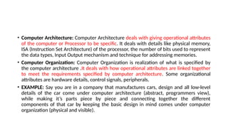
• Computer Architecture:Computer Architecture deals with giving operational attributes
of the computer or Processor to be specific. It deals with details like physical memory,
ISA (Instruction Set Architecture) of the processor, the number of bits used to represent
the data types, Input Output mechanism and technique for addressing memories.
• Computer Organization: Computer Organization is realization of what is specified by
the computer architecture .It deals with how operational attributes are linked together
to meet the requirements specified by computer architecture. Some organizational
attributes are hardware details, control signals, peripherals.
• EXAMPLE: Say you are in a company that manufactures cars, design and all low-level
details of the car come under computer architecture (abstract, programmers view),
while making it’s parts piece by piece and connecting together the different
components of that car by keeping the basic design in mind comes under computer
organization (physical and visible).
4.
Logic Gates
• Thelogic gates are the main structural part of a digital system.
• Logic Gates are a block of hardware that produces signals of binary 1
or 0 when input logic requirements are satisfied.
• Each gate has a distinct graphic symbol, and its operation can be
described by means of algebraic expressions.
• The seven basic logic gates includes: AND, OR, XOR, NOT, NAND, NOR,
and XNOR.
5.
AND GATE:
• TheAND gate produces the AND logic function, that is, the output is 1 if input A
and input B are both equal to 1; otherwise the output is 0.
• The algebraic symbol of the AND function is the same as
the multiplication symbol of ordinary arithmetic.
• We can either use a dot between the variables or concatenate the variables
without an operation symbol between them.
6.
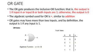
OR GATE
• TheOR gate produces the inclusive-OR function; that is, the output is
1 if input A or input B or both inputs are 1; otherwise, the output is 0
• The algebraic symbol used for OR is +, similar to addition
• OR gates may have more than two inputs, and by definition, the
output is 1 if any input is 1.
7.
NOT GATE:
• TheNOT gate is an electronic circuit which produces an inverted
version of the input at its output. It is also known as an Inverter.
• The algebraic symbol used for the logic complement is either a prime
or a bar over the variable symbol.
8.
NAND Gate
• TheNAND function is the complement of the AND function, as
indicated by the graphic symbol, which consists of an AND graphic
symbol followed by a small circle.
• The designation NAND is derived from the abbreviation of NOT-AND.
9.
NOR Gate
• TheNOR gate is the complement of the OR gate and uses an OR
graphic symbol followed by a small circle.
10.
Exclusive-OR Gate
• Theexclusive-OR gate has a graphic symbol similar to the OR gate except
for the additional curved line on the input side.
• The output of the gate is 1 if any input is 1 but excludes the combination
when both inputs are 1. It is similar to an odd function; that is, its output
is 1 if an odd number of inputs are 1.
11.
EXCLUSIVE-NOR
• The 'Exclusive-NOR'gate is a circuit that does the inverse operation to
the XOR gate. It will give a low output if one of its inputs is high but
not both of them. The small circle represents inversion.
12.
Boolean Algebra
• BooleanAlgebra is used to analyze and simplify the digital (logic)
circuits. It uses only the binary numbers i.e. 0 and 1. It is also called
as Binary Algebra or logical Algebra. Boolean algebra was invented
by George Boole in 1854.
13.
Boolean Laws
• Thereare six types of Boolean Laws.
1. Commutative law
• Any binary operation which satisfies the following expression is referred to as
commutative operation.
• Commutative law states that changing the sequence of the variables does not have
any effect on the output of a logic circuit.
2. Associative law
• This law states that the order in which the logic operations are performed is irrelevant
as their effect is the same.
14.
3. Distributive law
•Distributive law states the following condition.
4. AND law
• These laws use the AND operation. Therefore they are called as AND laws.
5. OR law
• These laws use the OR operation. Therefore they are called as OR laws.
6. INVERSION law
• This law uses the NOT operation. The inversion law states that double inversion of a
variable results in the original variable itself.
15.
• Example problem:
•Boolean function is represented as F = x + y'z. Construct Logical
diagram and truth table
Solution
The logic diagram for the Boolean function F = x + y'z can be represented as:
• The Boolean function F = x + y'z is transformed from an algebraic expression into a logic diagram composed
of AND, OR, and inverter gates.
• Inverter at input 'y' generates its complement y'.
• There is an AND gate for the term y'z, and an OR gate is used to combine the two terms (x and y'z).
• The variables of the function are taken to be the inputs of the circuit, and the variable symbol of the function
is taken as the output of the circuit.
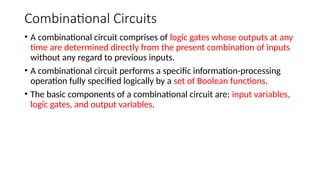
Combinational Circuits
• Acombinational circuit comprises of logic gates whose outputs at any
time are determined directly from the present combination of inputs
without any regard to previous inputs.
• A combinational circuit performs a specific information-processing
operation fully specified logically by a set of Boolean functions.
• The basic components of a combinational circuit are: input variables,
logic gates, and output variables.
18.
• The 'n'input variables come from an external source whereas the 'm' output variables go to an external
destination. In many applications, the source or destination are storage registers.
• The combinational Circuit consist of Half adder and Full adder.
19.
Half- Adder
• AHalf-adder circuit needs two binary inputs and two binary outputs.
• The input variable shows the augend and addend bits whereas the output variable
produces the sum and carry.
• We can understand the function of a half-adder by formulating a truth table.
• The truth table for a half-adder is:
• 'x' and 'y' are the two inputs, and S (Sum) and C (Carry)
are the two outputs.
• The Carry output is '0' unless both the inputs are 1.
• 'S' represents the least significant bit of the sum.
The logic diagram for a half-adder circuit can be
represented as:
20.
Full- Adder
• Thiscircuit needs three binary inputs and two binary outputs. The truth table for a full-
adder is:
• The truth table for a Full-adder is:
• Two of the input variable 'x' and 'y', represent the two
significant bits to be added.
• The third input variable 'z', represents the carry from
the previous lower significant position.
• The outputs are designated by the symbol 'S' for sum
and 'C' for carry.
The logic diagram for a half-adder circuit can be
represented as:
21.
Sequential Circuits
• Sequentialcircuits are digital circuits that store and use the previous state information
to determine their next state.
• Unlike combinational circuits, which only depend on the current input values to
produce outputs, sequential circuits depend on both the current inputs and the
previous state stored in memory elements.
1. Sequential circuits are commonly used in digital systems to implement state
machines, timers, counters, and memory elements. The memory elements in
sequential circuits can be implemented using flip-flops, which are circuits that
store binary values and maintain their state even when the inputs change.
2. There are two types of sequential circuits: finite state machines (FSMs) and
synchronous sequential circuits.
22.
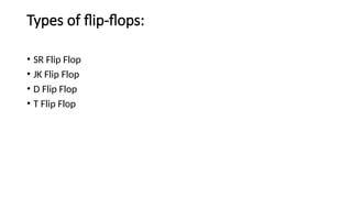
Flip Flops
• Flip-flopis a circuit that maintains a state until directed by input to
change the state.
• A basic flip-flop can be constructed using four-NAND or four-NOR gates.
• Flip flop is popularly known as the basic digital memory circuit. It has its
two states as logic 1(High) and logic 0(low) states.
• A flip flop is a sequential circuit which consist of single binary state of
information or data.
• The digital circuit is a flip flop which has two outputs and are of
opposite states. It is also known as a Bistable Multivibrator.