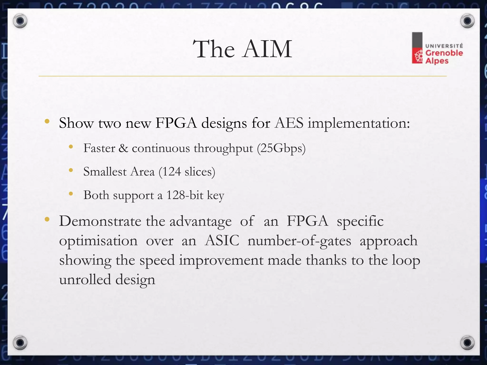
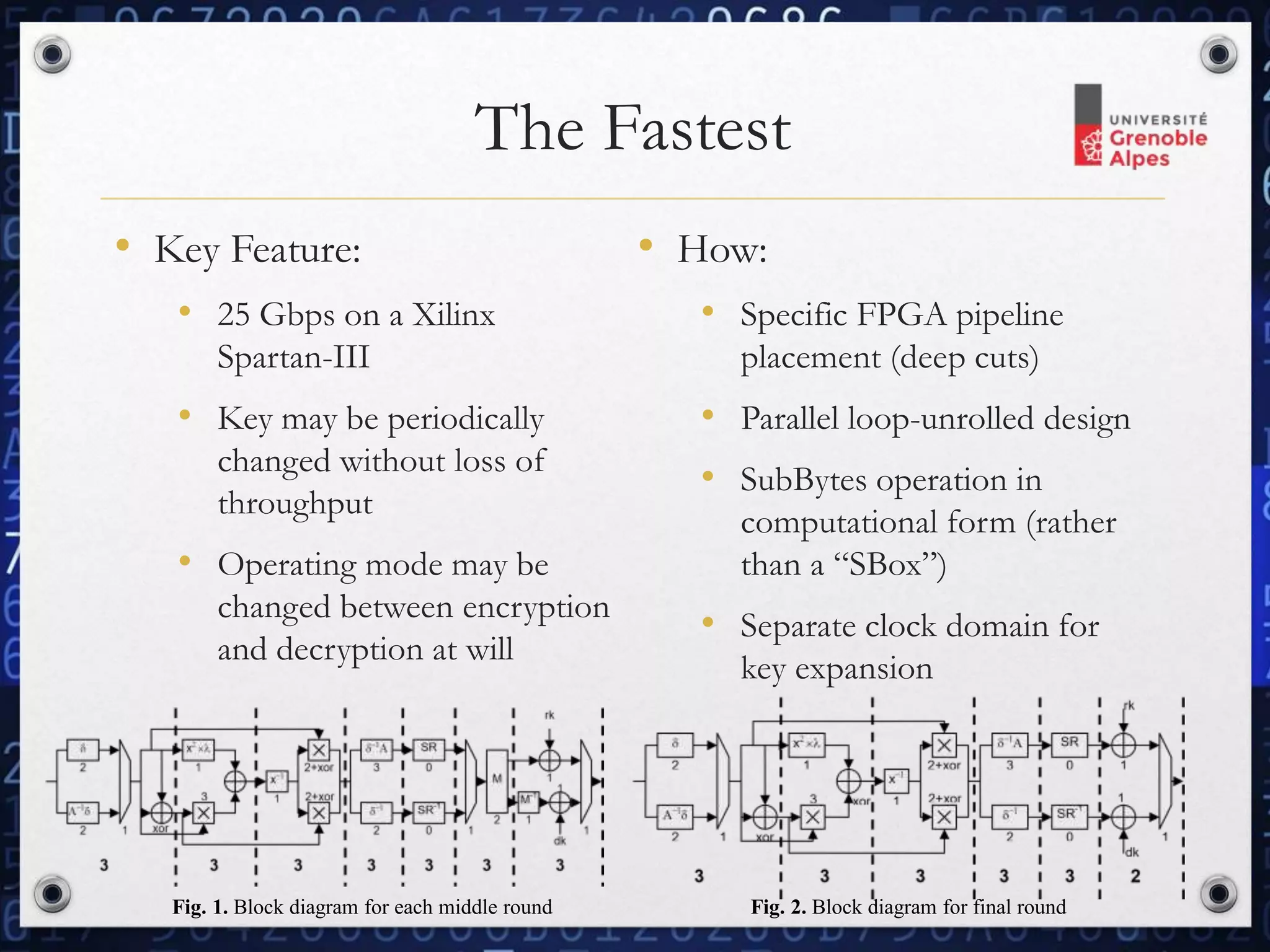
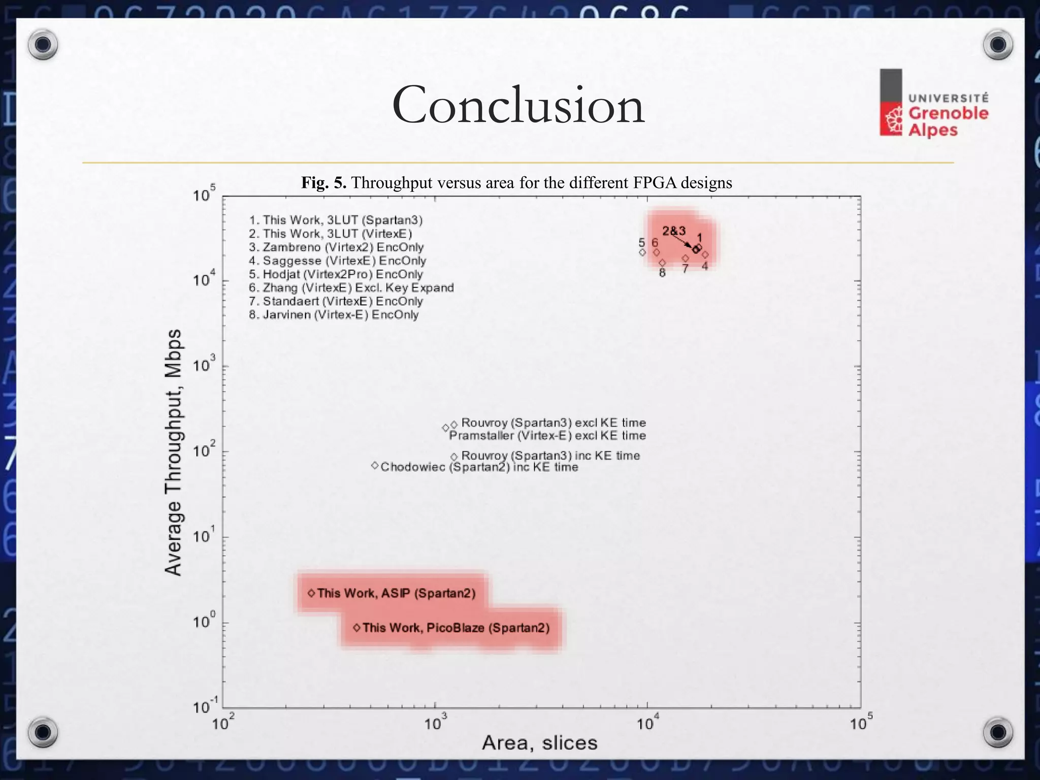
AES implementation
on FPGA
From the FASTEST to the SMALLEST
By
Tim Good and Mohammed Benaissa
Presented By Leonardo Antichi
The AIM
• Show two new FPGA designs for AES implementation:
• Faster & continuous throughput (25Gbps)
• Smallest Area (124 slices)
• Both support a 128-bit key
• Demonstrate the advantage of an FPGA specific
optimisation over an ASIC number-of-gates approach
showing the speed improvement made thanks to the loop
unrolled design
The Fastest
• Key Feature:
• 25 Gbps on a Xilinx
Spartan-III
• Key may be periodically
changed without loss
of throughput
• Operating mode may
be changed between
encryption and
decryption at will
• How:
• Specific FPGA pipeline
placement (deep cuts)
• Parallel loop-unrolled
design
• SubBytes operation in
computational form
(rather than a “SBox”)
• Separate clock domain
for key expansion
The Fastest
• Key Feature:
• 25 Gbps on a Xilinx
Spartan-III
• Key may be periodically
changed without loss of
throughput
• Operating mode may be
changed between encryption
and decryption at will
• How:
• Specific FPGA pipeline
placement (deep cuts)
• Parallel loop-unrolled design
• SubBytes operation in
computational form (rather
than a “SBox”)
• Separate clock domain for
key expansion
Fig. 1. Block diagram for each middle round Fig. 2. Block diagram for final round
The Smallest
• Key Feature:
• 124 slices only (60% of the
Xilinx Spartan-II device)
• 2,2 Mbps throughput
• How:
• Specific Processor
Architecture using 8-bit
data-path (ASIP)
• Subroutines and looping
• Pipelined design
permitting execution of a
new instruction every
cycle
• 360 bits of RAM
The Smallest
• Key Feature:
• 124 slices only (60% of the
Xilinx Spartan-II device)
• 2,2 Mbps throughput
• How:
• Specific Processor
Architecture using 8-bit
data-path (ASIP)
• Subroutines and looping
• Pipelined design permitting
execution of a new
instruction every cycle
• 360 bits of RAM
Fig. 3. ASIP Architecture
S-Box, 42
Fig. 4. Slice utilization versus design unit
Conclusion
Fig. 5. Throughput versus area for the different FPGA designs
Thank you
For your attention

AES Implementation on FPGA

  • 1.
    AES implementation on FPGA Fromthe FASTEST to the SMALLEST By Tim Good and Mohammed Benaissa Presented By Leonardo Antichi
  • 2.
    The AIM • Showtwo new FPGA designs for AES implementation: • Faster & continuous throughput (25Gbps) • Smallest Area (124 slices) • Both support a 128-bit key • Demonstrate the advantage of an FPGA specific optimisation over an ASIC number-of-gates approach showing the speed improvement made thanks to the loop unrolled design
  • 3.
    The Fastest • KeyFeature: • 25 Gbps on a Xilinx Spartan-III • Key may be periodically changed without loss of throughput • Operating mode may be changed between encryption and decryption at will • How: • Specific FPGA pipeline placement (deep cuts) • Parallel loop-unrolled design • SubBytes operation in computational form (rather than a “SBox”) • Separate clock domain for key expansion
  • 4.
    The Fastest • KeyFeature: • 25 Gbps on a Xilinx Spartan-III • Key may be periodically changed without loss of throughput • Operating mode may be changed between encryption and decryption at will • How: • Specific FPGA pipeline placement (deep cuts) • Parallel loop-unrolled design • SubBytes operation in computational form (rather than a “SBox”) • Separate clock domain for key expansion Fig. 1. Block diagram for each middle round Fig. 2. Block diagram for final round
  • 5.
    The Smallest • KeyFeature: • 124 slices only (60% of the Xilinx Spartan-II device) • 2,2 Mbps throughput • How: • Specific Processor Architecture using 8-bit data-path (ASIP) • Subroutines and looping • Pipelined design permitting execution of a new instruction every cycle • 360 bits of RAM
  • 6.
    The Smallest • KeyFeature: • 124 slices only (60% of the Xilinx Spartan-II device) • 2,2 Mbps throughput • How: • Specific Processor Architecture using 8-bit data-path (ASIP) • Subroutines and looping • Pipelined design permitting execution of a new instruction every cycle • 360 bits of RAM Fig. 3. ASIP Architecture S-Box, 42 Fig. 4. Slice utilization versus design unit
  • 7.
    Conclusion Fig. 5. Throughputversus area for the different FPGA designs
  • 8.

Editor's Notes

  • #3 THE AIM WHY FPGA? Expanding Design cost, risk, time to market Mass produced ARCHITECTURE CHOISES THE TWO DESIGNS The research objective is to explore the design space associated with the AES algorithm and in particular its FPGA (Field Programmable Gate Array ) hardware implementation. Why FPGA? Because FPGA has been expanding from its traditional role in prototyping to mainstream production. This change is being driven by commercial pressures to reduce design cost, risk and achieve a faster time to market. The Advances in technology have resulted in mask programmed mass produced versions of FPGA fabrics being offered by the leading manufacturers which, for some applications, remove the necessity to move prototype designs from FPGA to ASIC whilst still achieving a low unit cost. It is important also to underline that architectural choices for a given application are driven by the system requirements in terms of speed and the resources used and those can simply be viewed as throughput and area. For this porpoise two new FPGA designs are presented: The first is believed to be the fastest, achieving 25 Gb/s throughput using a Xilinx Spartan-III (XC3S2000) device, while, The second is believed to be the smallest and fits into a Xilinx Spartan-II (XC2S15) device, only requiring two block memories and 124 slices to achieve a throughput of 2.2 Mbps.
  • #4 DEEP CUT PIPELINE PLACEMENT UNROLLED DESIGN NO SBOX (Composite field arithmetic) FPGAs are particularly fast in terms of throughput when designs are implemented using deep pipeline cuts. The attainable speed is set by the longest path in the design so it is important to place the pipeline cuts such that the path lengths between the pipeline latches are balanced. First, the algorithm must be converted into a suitable form for deep pipelining. This is achieved by removing all the loops to form a loop-unrolled design where the data is moved through the stationary execution resources. On each clock cycle, a new item of data is input and progresses over numerous cycles through the pipeline resulting in the output of data each cycle, however, with some unavoidable latency. One of the key optimisations was to express the SubBytes operation in computational form rather than as a look-up table. Earlier implementations used the look-up table approach (the “S” box) but this resulted in an unbreakable delay due to the time required pass through the FPGA block memories. The FIPS-197 specification provided the mathematical derivation for SubBytes in terms of Galois Field (2^8) arithmetic. This was efficiently exploited by hardware implementations using composite field arithmetic which permitted a deeper level of pipelining and thus improved throughput.
  • #5 KEY CHANGES The high speed design presented here includes support for continued throughput during key changes for both encryption and decryption which previous pipelined designs have omitted.
  • #6 8bit design Longer clock less area 13546 cycles 18885 cycles ASIP 259 slices There already exist a number of good 32-bit based designs. In these designs the AES is implemented by breaking up a round into a number of smaller 32-bit wide operations. We decided to move to an 8 bit design increasing the clock necessary for completing the task but saving resources in terms of area occupied. This results in a final design using the PicoBlaze of 119 slices plus the block memories which are accounted for here by an equivalent number of slices (once again 32 bits per slice was used). The resulting design had an equivalent slice count of 452 and with a 90.2 MHz maximum clock. Key expansion followed by encipher took 13546 cycles and key expansion followed by decipher 18885 cycles. The average encipher-decipher throughput was 0.71 Mbps. An application specific instruction processor (ASIP) was developed based around an 8-bit datapath and minimal program ROM size. Minimisation of the ROM size resulted in a requirement to support subroutines and looping. This added area to the control portion of the design but the saving was made in terms of the size of the ROM. The total design, including an equivalent number of slices for the block memories only occupies 259 slices to give a throughput of 2.2Mbps.
  • #7 PROCESSOR DESIGN AREA (60%datapath 40%control) The datapath consisted of two processing units, the first to perform the SubBytes operation using resource shared composite field arithmetic and the second to perform multiply accumulate operations in Galois Field 2^8. A minimal set of instructions was developed (15 in total) to perform the operations required for the AES. The processor (Figure 3) used a pipelined design permitting execution of a new instruction every cycle. Figure 4 is a pie chart depicting the balance of area between the various design units. Of the processor hardware approx 60% of the area is required for the datapath and 40% for the control.
  • #8 THE FASTEST, APPLICATION THE SMALLEST, APPLICATION 32BIT These designs show the extremes of what is possible and have radically different applications In terms of speed to area ratio the unrolled designs perform the best as there is no controller overhead. However, such designs are very large and need a 1 – 2 million gate device but achieve throughputs up to 25 Gbps. These designs have applications in fixed infrastructure such as IPsec for e-commerce servers. The low area design described here achieves 2.2 Mbps which is sufficient for most wireless and home applications. The area required is small thus fundamentally low power so has utility in the future mobile area. The design requires just over half the available resources of the smallest available Spartan-II FPGA. The advantage of the 8-bit ASIP over the more traditional 8-bit microcontroller architecture (PicoBlaze) is shown by the approximate factor of three improvement in throughput and 40% reduction in area (including estimated area for memories). The 32-bit datapath designs occupy the middle ground between the two extremes and have utility where moderate throughput in the 100 – 200 Mbps is required.