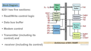
Block Diagram
8251 has five sections:
 Read/Write control logic
 Data bus buffer
 Modem control
 Transmitter (including its
control) and
 receiver (including its control)
What is the function of the Status Word Register of 8251?
Ans. The function of the status word register is to check or examine the preparedness of 8251 with regard
to transmission or reception of data.
Read/ Write Control logic
It contains three buffer registers:
 data buffer register
 control register
 status register
The six input signals are: CS , C/ D , WR, RD , RESET and CLK.
The particular 8251 is selected on CS signal going low. This pin is usually connected to a decoded
address bus. C/ D stands for control/data pin. When this pin is high, either the control register or status
register is selected and when low, data bus buffer is selected.
The control register and
the status register are
distinguished by WR and
RD signals,
respectively.
The figure below shows
how the three registers:
data buffer register,
control register
and status register are
accessed by making
respectively.
Transmitter Section
The transmitter section consists of three
blocks—transmitter buffer register, output
register and the transmitter control logic
block. The CPU deposits (when TXRDY = 1,
meaning that the transmitter buffer register is
empty) data into the transmitter buffer
register, which is subsequently put into the
output register (when TXE = 1, meaning that
the output buffer is empty). In the output
register, the eight bit data is converted into
serial form and comes out via TXD pin. The
serial data bits are preceded by START bit
and succeeded by STOP bit, which are
known as framing bits. But this happens only
if
transmitter is enabled and the CTS is low.
TXC signal is the transmitter clock signal
which controls the bit rate on the TXD line
(output line). This clock frequency can be 1,
16 or 64 times the baud.
Receiver Section
The receiver section consists of three blocks —
receiver buffer register, input register and the
receiver control logic block. Serial data from
outside world is delivered to the input register
via RXD line, which is subsequently put into
parallel form and placed in the receiver buffer
register. When this register is full, the RXRDY
(receiver ready) line becomes high. This line is
then used either to interrupt the MPU or to
indicate its own status. MPU then accepts the
data from the register.
RXC line stands for receiver clock. This clock
signal controls the rate at which bits are received
by the input register. The clock can be set to 1,
16 or 64 times the baud in the asynchronous
mode.
How does the CPU know that the transmitter buffer is empty?
Ans. The CPU knows about the same by
z examining the TXRDY line of the transmitter.
z examining D0 bit of the status word.
10. When the TxD line goes into the MARKING (HIGH) state? Ans. It becomes high in the following
cases:
z a RESET is received by 8251.
z transmitter is empty.
z transmitter is not enabled.
z CTS is off.
How the transmitter is enabled?
Ans. The transmitter is enabled by setting bit D0 of the command
instruction word.
Why modems (modulators-demodulators) are used in case of digital transmission of data?
Ans. The term ‘modem’ stands for modulator—demodulator. In a communication environment, two modems
are used—one at the transmitting end side and one at the receiving end side. Modems are generally called
DCE (Data Communication Equipment).
High frequency digital signals require a very wide transmission channel bandwidth which makes the system
very costly. However, existing telephone line facilities (which carry analog signals in the range of 40 Hz to 4
KHz) can be used to transmit such high frequency digital signals. A modem converts a digital signal into
audio tone frequencies (at the transmitting end side) and reconverts this audio frequencies into h.f. digital
signals (at the receiving end side)—and it utilises Frequency Shift Keying (FSK) for this purpose. Thus a
modem converts a logical ‘1’ to 1200 Hz and ‘0’ to 2200 Hz audio frequency. These signals are then
transmitted over a telephone line over a ‘carrier’. The inverse operation is done at the receiving end side.
Draw the block diagram of a DTE-DCE interface in a communication environment.
Digital data is delivered at the
DTE (may be 8251) in parallel
form, which is then converted into
serial form and sent to DCE via
RS-232 cable. The DCE (a
modem) output is an audio signal
carried through a telephone line.

8251 Universal Synchronous Asynchronous T.pdf

  • 1.
    Block Diagram 8251 hasfive sections:  Read/Write control logic  Data bus buffer  Modem control  Transmitter (including its control) and  receiver (including its control)
  • 2.
    What is thefunction of the Status Word Register of 8251? Ans. The function of the status word register is to check or examine the preparedness of 8251 with regard to transmission or reception of data.
  • 3.
    Read/ Write Controllogic It contains three buffer registers:  data buffer register  control register  status register The six input signals are: CS , C/ D , WR, RD , RESET and CLK. The particular 8251 is selected on CS signal going low. This pin is usually connected to a decoded address bus. C/ D stands for control/data pin. When this pin is high, either the control register or status register is selected and when low, data bus buffer is selected.
  • 4.
    The control registerand the status register are distinguished by WR and RD signals, respectively. The figure below shows how the three registers: data buffer register, control register and status register are accessed by making respectively.
  • 5.
    Transmitter Section The transmittersection consists of three blocks—transmitter buffer register, output register and the transmitter control logic block. The CPU deposits (when TXRDY = 1, meaning that the transmitter buffer register is empty) data into the transmitter buffer register, which is subsequently put into the output register (when TXE = 1, meaning that the output buffer is empty). In the output register, the eight bit data is converted into serial form and comes out via TXD pin. The serial data bits are preceded by START bit and succeeded by STOP bit, which are known as framing bits. But this happens only if transmitter is enabled and the CTS is low. TXC signal is the transmitter clock signal which controls the bit rate on the TXD line (output line). This clock frequency can be 1, 16 or 64 times the baud.
  • 6.
    Receiver Section The receiversection consists of three blocks — receiver buffer register, input register and the receiver control logic block. Serial data from outside world is delivered to the input register via RXD line, which is subsequently put into parallel form and placed in the receiver buffer register. When this register is full, the RXRDY (receiver ready) line becomes high. This line is then used either to interrupt the MPU or to indicate its own status. MPU then accepts the data from the register. RXC line stands for receiver clock. This clock signal controls the rate at which bits are received by the input register. The clock can be set to 1, 16 or 64 times the baud in the asynchronous mode.
  • 7.
    How does theCPU know that the transmitter buffer is empty? Ans. The CPU knows about the same by z examining the TXRDY line of the transmitter. z examining D0 bit of the status word. 10. When the TxD line goes into the MARKING (HIGH) state? Ans. It becomes high in the following cases: z a RESET is received by 8251. z transmitter is empty. z transmitter is not enabled. z CTS is off. How the transmitter is enabled? Ans. The transmitter is enabled by setting bit D0 of the command instruction word.
  • 8.
    Why modems (modulators-demodulators)are used in case of digital transmission of data? Ans. The term ‘modem’ stands for modulator—demodulator. In a communication environment, two modems are used—one at the transmitting end side and one at the receiving end side. Modems are generally called DCE (Data Communication Equipment). High frequency digital signals require a very wide transmission channel bandwidth which makes the system very costly. However, existing telephone line facilities (which carry analog signals in the range of 40 Hz to 4 KHz) can be used to transmit such high frequency digital signals. A modem converts a digital signal into audio tone frequencies (at the transmitting end side) and reconverts this audio frequencies into h.f. digital signals (at the receiving end side)—and it utilises Frequency Shift Keying (FSK) for this purpose. Thus a modem converts a logical ‘1’ to 1200 Hz and ‘0’ to 2200 Hz audio frequency. These signals are then transmitted over a telephone line over a ‘carrier’. The inverse operation is done at the receiving end side.
  • 9.
    Draw the blockdiagram of a DTE-DCE interface in a communication environment. Digital data is delivered at the DTE (may be 8251) in parallel form, which is then converted into serial form and sent to DCE via RS-232 cable. The DCE (a modem) output is an audio signal carried through a telephone line.