The document discusses Boolean algebra, including laws of Boolean algebra, De Morgan's theorems, minimizing Boolean expressions, and converting between AND/OR/invert logic and NAND/NOR logic. It defines Boolean algebra as the mathematics of digital logic using true/false or high/low values. Boolean expressions are formed using common operators like AND, OR, and NOT. De Morgan's theorems allow exchanging ANDs and ORs using inverters. Methods are provided for simplifying Boolean expressions and converting between logic types using steps like adding or removing inverters at points with polarity changes.


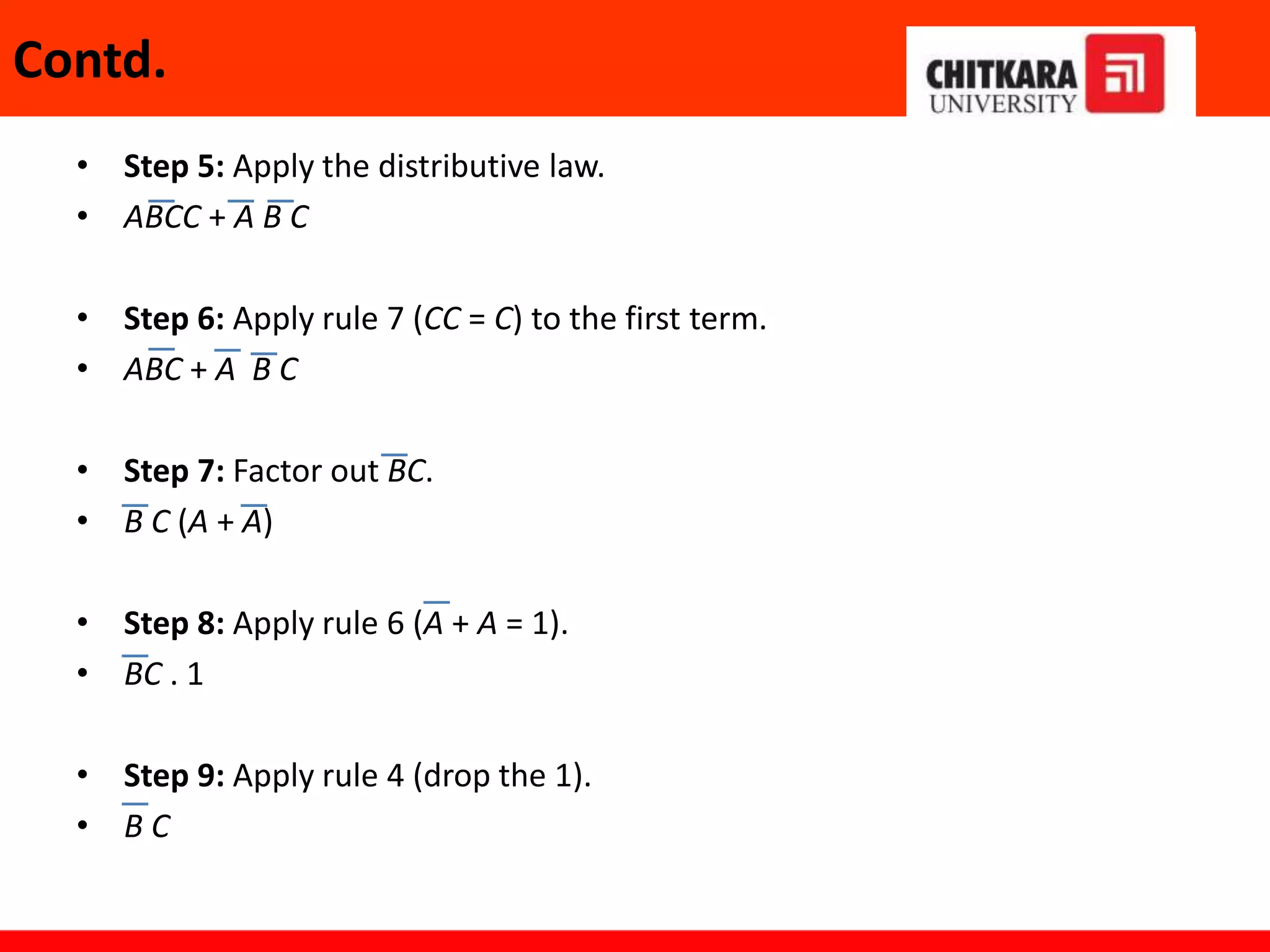
![Contd.
Example 2: Simplify the following Boolean expression: [A B (C + B D) + A B] C
Apply the distributive law to the terms within the brackets.
Step 1: (ABC + ABBD + A B)C
Step 2: Apply rule 8 (BB = 0) to the second term within the parentheses.
(ABC + A . 0 . D + A B) C
Step 3: Apply rule 3 (A . 0 . D = 0) to the second term within the parentheses.
(ABC + 0 + A B) C
Step 4: Apply rule 1 (drop the 0) within the parentheses.
(ABC + A B) C](https://image.slidesharecdn.com/3-230115063254-ca1b922d/75/3-Boolean-Algebra-pptx-10-2048.jpg)
![Activity 2
Reduce the following expressions:
1. F= A+B [AC+(B+C)D]
2. F= (B+BC) (B+BC)(B+D)
3. Show that ABC+B+BD+ABD+AC = B+C](https://image.slidesharecdn.com/3-230115063254-ca1b922d/75/3-Boolean-Algebra-pptx-12-2048.jpg)


![Chapter 3 computer Boolean Algebra 2[1].pptx](https://cdn.slidesharecdn.com/ss_thumbnails/chapter3booleanalgebra21-240928031107-5861eb7e-thumbnail.jpg?width=640&height=640&fit=bounds)