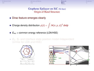
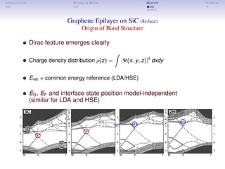
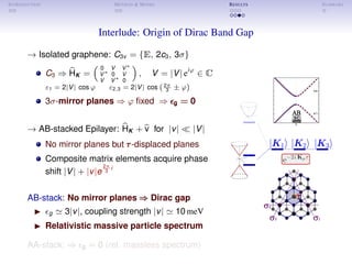
This study uses density functional theory calculations with a hybrid functional approach to compare graphene epitaxial layers on cubic and hexagonal silicon carbide polytypes. The results show that while the Dirac point shifts relative to the bulk bands with different polytypes, the essential Dirac feature of the graphene layer is preserved. A uniform Fermi velocity and similar carrier doping levels are found. Additionally, a small substrate-mediated band gap of 25-40 meV is induced at the Dirac point for all polytypes due to the broken symmetry of the graphene-SiC interface.

![INTRODUCTION METHOD & MODEL RESULTS SUMMARY
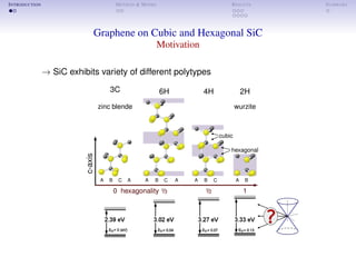
Graphene on Cubic and Hexagonal SiC
Calculational Method
Problem 1) Band gap deficiency of LDA-functional
Combined LDA-/HSE hybrid functional approach
(Heyd-Scuseria-Ernzerhof)
1
◦ Admix fraction of nonlocal HF-type exchange
EHSE
xc = EPBE
xc + 1
4
EHF
x − EPBE
x
◦ Screened interaction reduces calculational expense
1
r
≡ erfc(ωr)
r
short-range
+ erf(ωr)
r
long-range
Density functional program package VASP2
XC-functional L(S)DA HSE06 hybrid
Cut-off energy [eV] 520 eV 420 eV
Γ-centered k-sampling 9x9x1 6x6x1
PAW pseudo-potentials CA PBE
[1] Heyd et al., J.Chem.Phys. (2003) [2] Kresse and Furthmüller, PRB (1996)](https://image.slidesharecdn.com/aba66b1c-5070-4a9d-aaae-71347da6f578-160224163832/85/2013_Talk-Regensburg-DPG-4-320.jpg)
![INTRODUCTION METHOD & MODEL RESULTS SUMMARY
Graphene on Cubic and Hexagonal SiC
Structural Access
Problem 2) Incommensurable lattices
Si-face (6
√
3×6
√
3)R30 buffer layer1
C-face no buffer,2,3 mutually rotated layer4
(
√
3×
√
3)R30 Model
computationally tractable
correct description of graphene on Si-face5,6
◦ covalent interface bonding
◦ correct epilayer distance
◦ strained graphene interface has minor effect7
⇒ Focus on the Si-face
PRL 99, 076802 (2007)
[1] Otha et al., Science (2006) [2] Emtsev et al., PRB (2008) [3] Hiebel et al., PRB (2009)
[4] Haas et al., PRL (2008) [5] Mattausch et al., PRL (2007) [6] Varchon et al., PRL (2007)
[7] Pankratov et al., PRB (2010)](https://image.slidesharecdn.com/aba66b1c-5070-4a9d-aaae-71347da6f578-160224163832/85/2013_Talk-Regensburg-DPG-5-320.jpg)
![INTRODUCTION METHOD & MODEL RESULTS SUMMARY
Graphene Epilayer on SiC (Si-face)
Dirac Point Position
ED, EF shift systematically with hexagonality
HSE in good agreement with experiments
|EF − ED| ∼= const. ⇒ ne− 5.6 · 1013
cm−2
SiC EHSE
D − EHSE
V [eV] EExp
D − EExp
V [eV] EF − ED [eV]
3C 1.48 0.62
6H 1.90 2.25 [1] 0.63
4H 2.53 2.91±±±0.1 [2] 0.61
2H 2.39 0.62
[1] Ristein et al., PRL 108, 246104 (2012) [2] Sonde et al., PRB 80, 241406 (2009)](https://image.slidesharecdn.com/aba66b1c-5070-4a9d-aaae-71347da6f578-160224163832/85/2013_Talk-Regensburg-DPG-8-320.jpg)
![INTRODUCTION METHOD & MODEL RESULTS SUMMARY
Graphene Epilayer on SiC (Si-face)
Dirac Band Gap
Dirac band gap εg = 25 ∼ 40 meV same for HSE and LDA
Similar small εg for strain-free 5x5 structure1
Upper experimental limit given by ARPES resolution (40 ∼ 50 meV)
SiC HSE
g [meV]
LDA
g [meV]
3C 41.4 36.7
6H 39.9 35.4
4H 28.0 26.3
2H 33.9 32.9
[1] Pankratov et al., PRB 82, 121416R (2010)](https://image.slidesharecdn.com/aba66b1c-5070-4a9d-aaae-71347da6f578-160224163832/85/2013_Talk-Regensburg-DPG-9-320.jpg)
![INTRODUCTION METHOD & MODEL RESULTS SUMMARY
Summary - Graphene on Different SiC Polytypes
Ab initio Calculations with Combined LDA and HSE06 Hybrid Functional Approach
1 Influence of substrate polytypes on Epilayer?
2 Dirac band alignment relative to bulk bands?
Preservation of essential epilayer Dirac feature
Uniform Fermi-velocity, similar n-doping (Fermi-pinning)
Substrate-mediated Dirac band gap1
(εg = 25 ∼ 40 meV)
ED, EF shift systematically relative to VBM
HSE06 - good agreement with experimental data, LDA - correctly
corroborates trends
[1] Pankratov et al., PRB 86, 155432 (2012)](https://image.slidesharecdn.com/aba66b1c-5070-4a9d-aaae-71347da6f578-160224163832/85/2013_Talk-Regensburg-DPG-15-320.jpg)


![Lecture 3 d_equilibrium [compatibility mode]](https://cdn.slidesharecdn.com/ss_thumbnails/lecture3dequilibriumcompatibilitymode-160126133858-thumbnail.jpg?width=640&height=640&fit=bounds)