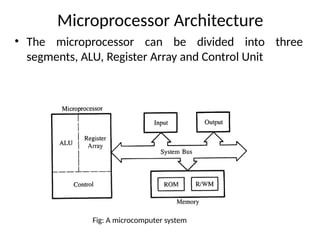
Microprocessor Architecture
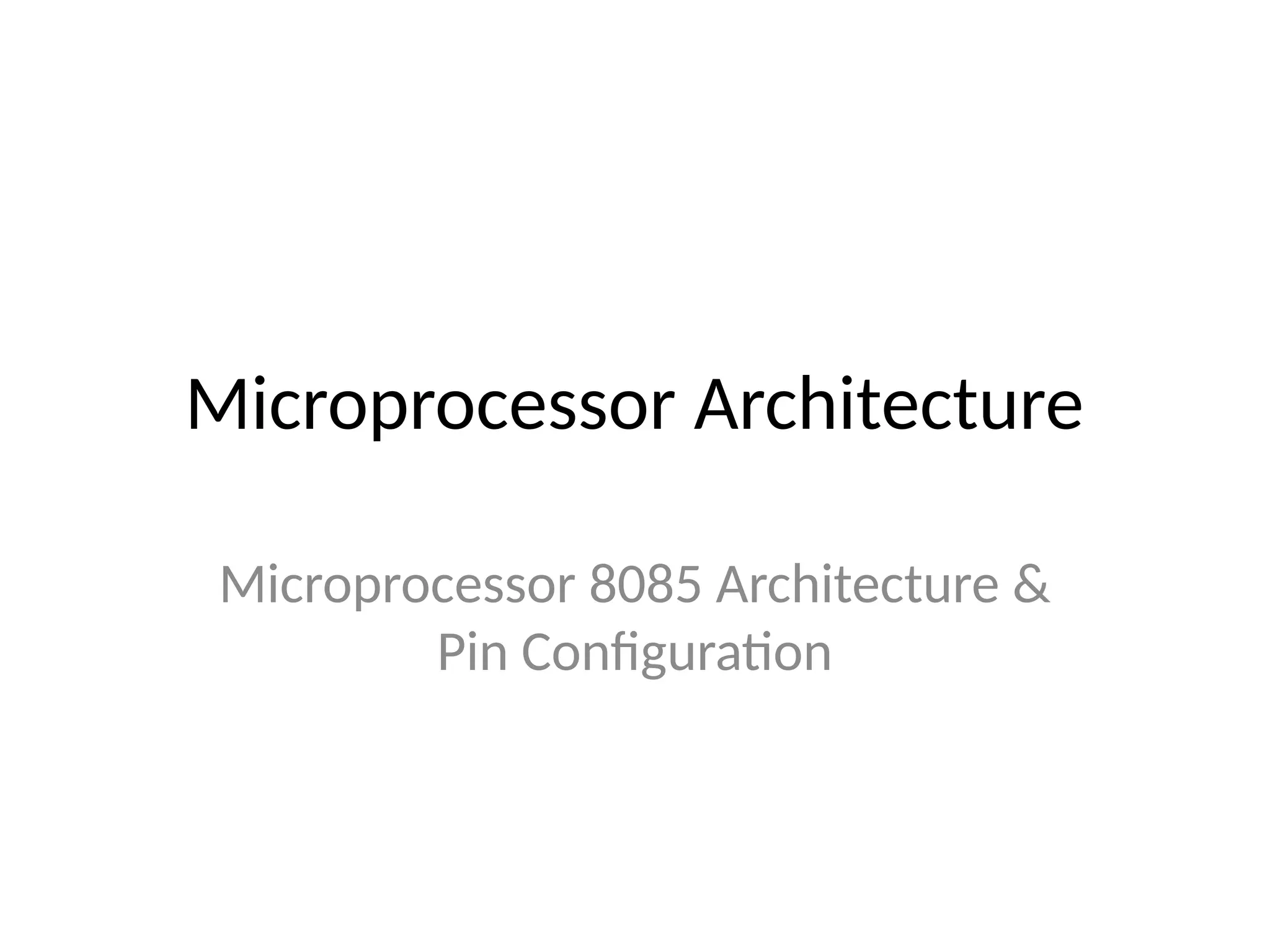
• Amicrocomputer system consists of four components,
the microprocessor, memory and Input and Output
devices.
• The microprocessor manipulates data, controls the
timing of various operations, and communicates with
peripherals , memory and I/O.
Fig: A microcomputer system
3.
Microprocessor Architecture
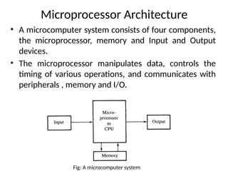
• Theinternal logic design of the microprocessor called
its architecture, determines how and when various
operations are performed by the microprocessor.
Fig: A microcomputer system
4.
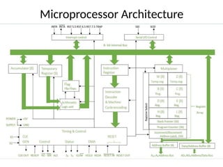
Microprocessor Architecture
• Themicroprocessor can be divided into three
segments, ALU, Register Array and Control Unit
Fig: A microcomputer system
5.
Microprocessor Architecture
• ALUperforms arithmetical and logical operations on the
data received from the memory or an input device.
• Register array consists of registers identified by letters
like B, C, D, E, H, L and accumulator.
• These registers are primarily used to store data
temporarily during the execution of a program.
• Some of the registers are accessible to the user through
instructions.
• The control unit controls the flow of data and
instructions within the computer.
• The control unit provides the necessary timing and
control signals to all the operations in the
microcomputer.
6.
Microprocessor Architecture
• ALUperforms arithmetical and logical operations on the
data received from the memory or an input device.
• Register array consists of registers identified by letters
like B, C, D, E, H, L and accumulator.
• These registers are primarily used to store data
temporarily during the execution of a program.
• Some of the registers are accessible to the user through
instructions.
• The control unit controls the flow of data and
instructions within the computer.
• The control unit provides the necessary timing and
control signals to all the operations in the
microcomputer.
7.
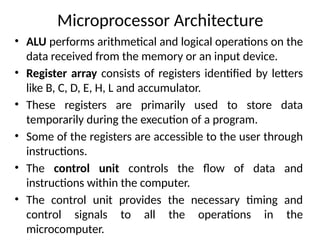
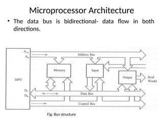
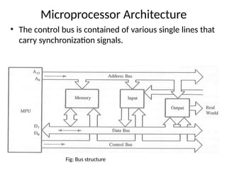
Microprocessor Architecture
• Thebus carries bits (data) between the
microprocessor and the memory and peripheral
devices.
Fig: Bus structure
8.
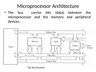
Microprocessor Architecture
• Theaddress bus is unidirectional- bits flow in one
directions- from microprocessor to peripheral devices.
Fig: Bus structure
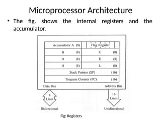
Microprocessor Architecture
• Accumulator:It is an 8-bit register used to perform
arithmetic, logical, I/O & LOAD/STORE operations. It is
connected to internal data bus & ALU.
Fig: Registers
13.
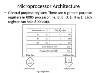
Microprocessor Architecture
• Generalpurpose register: There are 6 general purpose
registers in 8085 processor, i.e. B, C, D, E, H & L. Each
register can hold 8-bit data.
Fig: Registers
14.
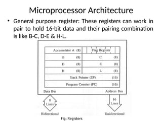
Microprocessor Architecture
• Generalpurpose register: These registers can work in
pair to hold 16-bit data and their pairing combination
is like B-C, D-E & H-L.
Fig: Registers
15.
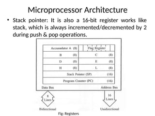
Microprocessor Architecture
• Stackpointer: It is also a 16-bit register works like
stack, which is always incremented/decremented by 2
during push & pop operations.
Fig: Registers
16.
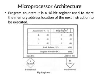
Microprocessor Architecture
• Programcounter: It is a 16-bit register used to store
the memory address location of the next instruction to
be executed.
Fig: Registers
17.
Microprocessor Architecture
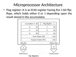
• Flagregister: It is an 8-bit register having five 1-bit flip-
flops, which holds either 0 or 1 depending upon the
result stored in the accumulator.
Fig: Registers
18.
Microprocessor Architecture
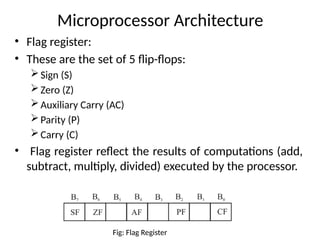
• Flagregister:
• These are the set of 5 flip-flops:
Sign (S)
Zero (Z)
Auxiliary Carry (AC)
Parity (P)
Carry (C)
• Flag register reflect the results of computations (add,
subtract, multiply, divided) executed by the processor.
Fig: Flag Register
Microprocessor Architecture
• ifCF =1, then the result is positive and if CF =0, then
the result is negative.
• Since, the 8085 processor complements the carry after
subtraction, here if CF = 0, then the result is positive
and if CF = 1, then the result is negative.
• If the result is negative, then it will be in 2's
complement form.
22.
Microprocessor Architecture
• ifCF =1, then the result is positive and if CF =0, then
the result is negative.
• Since, the 8085 processor complements the carry after
subtraction, here if CF = 0, then the result is positive
and if CF = 1, then the result is negative.
• If the result is negative, then it will be in 2's
complement form.
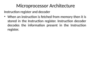
Microprocessor Architecture
Instruction registerand decoder
• When an instruction is fetched from memory then it is
stored in the Instruction register. Instruction decoder
decodes the information present in the Instruction
register.
25.
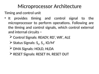
Microprocessor Architecture
Timing andcontrol unit
• It provides timing and control signal to the
microprocessor to perform operations. Following are
the timing and control signals, which control external
and internal circuits −
Control Signals: READY, RD’, WR’, ALE
Status Signals: S0, S1, IO/M’
DMA Signals: HOLD, HLDA
RESET Signals: RESET IN, RESET OUT
26.
Microprocessor Architecture
Interrupt control
•As the name suggests it controls the interrupts during
a process. When a microprocessor is executing a main
program and whenever an interrupt occurs, the
microprocessor shifts the control from the main
program to process the incoming request. After the
request is completed, the control goes back to the
main program.
• There are 5 interrupt signals in 8085 microprocessor:
INTR, (INTA)’ RST 7.5, RST 6.5, RST 5.5, TRAP.
Address Bus andData Bus
• A8 - A15 (Output):
• These are address bus and are used for the most
significant bits of the memory address or 8-bits of I/O
address. A8 –A15 are unidirectional buses.
• AD0 - AD7 (Input/output):
• These are time multiplexed address/data bus i.e. they
serve dual purpose.
• They are used for the least significant 8 bits of the
memory address or I/O address during the first cycle.
• Again they are used for data during 2nd and 3rd clock
cycles.
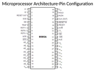
Microprocessor Architecture-Pin Configuration
30.
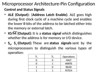
Control and StatusSignals
• ALE (Output): (Address Latch Enable). ALE goes high
during first clock cycle of a machine cycle and enables
the lower 8-bits of the address to be latched either into
the memory or external latch.
• IO/M (Output): It is a status signal which distinguishes
whether the address is for memory or I/O device.
• S0, S1 (Output): These are status signals sent by the
microprocessors to distinguish the various types of
operation:
Microprocessor Architecture-Pin Configuration
S1 S0 Operations
0 0 HALT
0 1 WRITE
1 0 READ
1 1 FETCH
31.
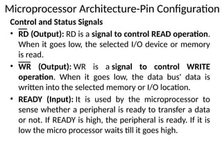
Control and StatusSignals
• RD (Output): RD is a signal to control READ operation.
When it goes low, the selected I/O device or memory
is read.
• WR (Output): WR is a signal to control WRITE
operation. When it goes low, the data bus' data is
written into the selected memory or I/O location.
• READY (Input): It is used by the microprocessor to
sense whether a peripheral is ready to transfer a data
or not. If READY is high, the peripheral is ready. If it is
low the micro processor waits till it goes high.
Microprocessor Architecture-Pin Configuration
32.
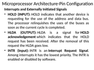
Interrupts and ExternallyInitiated Signals
• HOLD (INPUT): HOLD indicates that another device is
requesting for the use of the address and data bus.
The processor relinquishes the uses of the buses as
soon as the current cycle is completed.
• HLDA (OUTPUT): HLDA is a signal for HOLD
acknowledgement which indicates that the HOLD
request has been received. After the removal of this
request the HLDA goes low.
• INTR (Input): INTR is an Interrupt Request Signal.
Among interrupts it has the lowest priority. The INTR is
enabled or disabled by software.
Microprocessor Architecture-Pin Configuration
33.
Interrupts and ExternallyInitiated Signals
• INTA (Output): INTA is an interrupt
acknowledgement sent by the microprocessor after
INTR is received.
• RST 5.5, 6.5, 7.5 and TRAP (Inputs): These all are
interrupts.
• The TRAP has the highest priority among interrupts.
The order of priority of interrupts is as follows:
TRAP (Highest priority)
RST 7.5
RST 6.5
RST 5.5
INTR (Lowest priority).
Microprocessor Architecture-Pin Configuration
34.
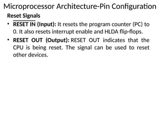
Reset Signals
• RESETIN (Input): It resets the program counter (PC) to
0. It also resets interrupt enable and HLDA flip-flops.
• RESET OUT (Output): RESET OUT indicates that the
CPU is being reset. The signal can be used to reset
other devices.
Microprocessor Architecture-Pin Configuration
35.
Clock Signals
• X1,X2 (Input): X1 and X2 are terminals to be connected
to an external crystal oscillator which drives an
internal circuitry of the microprocessor.
• It is used to produce a suitable clock for the operation
of microprocessor.
• CLK (Output): CLK is a clock output for user, which can
be used as the system clock for other digital ICs. Its
frequency is same at which processor operates.
Microprocessor Architecture-Pin Configuration
36.
Serial I/O Signals
•SID (Input): SID is data line for serial input. The data
on this line is loaded into the seventh bit of the
accumulator when RIM instruction is executed.
• SOD (Output): SOD is a data line for serial output. The
seventh bit of the accumulator is output on SOD line
when SIM instruction is executed.
Power Supply
• Vcc : +5 Vlots supply
• Vss : ground reference
Microprocessor Architecture-Pin Configuration
37.
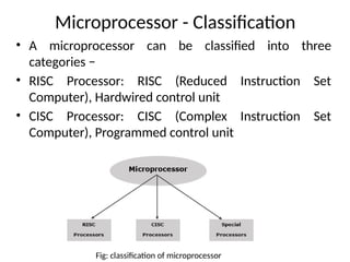
Microprocessor - Classification
•A microprocessor can be classified into three
categories −
• RISC Processor: RISC (Reduced Instruction Set
Computer), Hardwired control unit
• CISC Processor: CISC (Complex Instruction Set
Computer), Programmed control unit
Fig: classification of microprocessor
38.
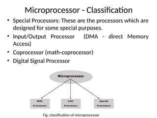
Microprocessor - Classification
•Special Processors: These are the processors which are
designed for some special purposes.
• Input/Output Processor (DMA - direct Memory
Access)
• Coprocessor (math-coprocessor)
• Digital Signal Processor
Fig: classification of microprocessor