1-AN Introduction to Basic Electronics Course.pdf
•
0 likes•39 views
Introduction to Basic electronic
Report
Share
Report
Share
Download to read offline

Recommended
Synopsis
This document describes a comparative study of ZnO layers grown using molecular beam epitaxy (MBE) and radio frequency (RF) sputtering techniques. It discusses the properties and applications of ZnO, the deposition techniques, and characterization methods like current-voltage measurement, deep level transient spectroscopy, and photoluminescence spectroscopy. The goals of the study are to understand defects in ZnO grown by different methods and correlate growth parameters with material properties to enable high-performance ZnO-based optical and electronic devices.
Fdp report
A three day workshop on PN-Junction and BJT devices was held from April 11-13 at VCET in Puttur. The workshop consisted of five sessions covering topics ranging from the classification of solids and quantum numbers to PN junction formation, bias conditions, and BJT operation. Dr. P. Subbanna Bhat began by emphasizing the importance of continuous learning. Sessions explained the theory behind semiconductor diodes and PN junctions, as well as reverse breakdown voltage, BJT terminals and regions of operation, and rectifier circuits. Participants found the workshop very helpful in understanding these fundamental semiconductor concepts and devices.
Chapter 07.ppt Electrical conduction
This chapter discusses electrical conduction processes in materials and semiconductor devices. It begins by describing conduction in metals, semiconductors, and doped semiconductors. Next, it covers the p-n junction, including the formation of a space-charge layer and drift and diffusion currents. The characteristics of the p-n junction and diode are then explained. The chapter concludes by discussing maximum power dissipation and voltage limitations in diodes due to avalanche and Zener breakdown.
Electronics-I Theory.doc
This document outlines the course details for Electronics-I, a 3 credit hour course offered by the BS Physics Department at NFC Institute of Engineering and Technology. The course covers topics related to amplifiers, oscillators, modulation, and integrated circuits. Student assessment will include sessional tests, quizzes, assignments, attendance, presentations, a midterm exam, and an end term exam. The textbook is Electronics Fundamentals by Thomas L. Floyd and the reference book is Basic Electronics by B. Grob. The course includes a laboratory component.
UROP Symposium
This document summarizes research characterizing the electrical properties of different isoforms of the reflectin protein, which may have applications in bioelectronic devices. Protonic transistors were fabricated using reflectin isoforms A1, A2, and B1 as the active material. All isoforms showed increased current with proton-injecting palladium hydride electrodes and increasing humidity, indicating proton conduction. Field effect tests also supported proton conduction. Future work may include integrating these transistors with living materials or engineering optimized isoforms through selective breeding.
CV_Nihar
This document contains the curriculum vitae of Nihar R. Pradhan, who is currently a postdoctoral research associate at the National High Magnetic Field Laboratory in Tallahassee, Florida. His research focuses on nanotechnology, including the synthesis and characterization of two-dimensional materials like transition metal dichalcogenides. Some of his work involves fabricating field-effect transistors from these materials and investigating their electrical and optical properties. He has a Ph.D. in Physics from Worcester Polytechnic Institute and several years of experience as a postdoctoral researcher.
Synopsis : Bismuth Sodium Titanate ( A lead free Ferroelectric Material
Synopsis : Bismuth Sodium Titanate ( A lead free Ferroelectric MaterialNational Tsing Hua University
This document summarizes a thesis submitted for a Master's degree in nano-optoelectronics. The thesis focuses on synthesizing and characterizing bismuth sodium titanate (BNT), a lead-free ferroelectric material. BNT is studied as an alternative to lead zirconate titanate (PZT), which is widely used but toxic. The thesis will synthesize BNT using solid-state and sol-gel methods, characterize its structure and properties, and compare the results. Characterization tools like XRD, SEM, and dielectric measurements will be used. If successful, BNT could replace PZT in applications like sensors and actuators while avoiding lead's toxicity issues.Ews ppt Sushama Gavarskar
The document describes an electronics workshop for students. It outlines the mission of the department, which is to provide good technical education and enhance competency through infrastructure, resources, teaching, and committed faculty. It also aims to provide platforms for developing professionalism and ethics in students. The workshop aims to create a strong foundation to enable students' career choices. The document then lists the experiments covered in the workshop, including studying basic electronic components like resistors, capacitors, inductors, diodes, and transistors. It provides details on one experiment to identify specifications of components by referring to datasheets and understand their applications.
Osmania University BSc Electronics Syllabus
This document outlines the syllabus for a B.Sc. in Electronics program under the Choice Based Credit System at Osmania University. It provides details of the course structure over six semesters, including the title and credits of theory and practical papers each semester. The syllabus and expected learning outcomes are described for core papers in circuits, electronic devices, analog and digital circuits, and communication systems. It also lists reference books and websites for more information.
Syllabus of b.sc_electronics_semester_pattern2013
This document contains information about various topics covered in B.Sc Electronics Semester 1. It includes 4 units for Paper 1 on Electronic Components, Network Theorems and DC circuits. It also includes 4 units for Paper 2 on fundamentals of digital electronics covering number systems, logic gates, Karnaugh maps and combinational logic circuits. It lists practical experiments related to both papers. It provides reference books for both subjects. Overall, the document outlines the syllabus, topics and experiments for the first semester of a B.Sc Electronics degree.
winston_academic_cv
Winston Frias Pombo is a physicist currently working at the University of Saskatchewan. He has experience in theoretical and computational physics, with a focus on plasma physics, electromagnetism, and wave propagation. His research has been published in leading scientific journals and presented at major conferences. He holds a PhD in Physics from the University of Saskatchewan and is looking for research positions where he can continue developing his computational skills and applying them to real-world problems.
Electrical Measurements for Semiconducting Devices
The document discusses electrical measurements for semiconducting devices. It describes current-voltage (I-V) characteristics and capacitance-voltage (C-V) characteristics, which are important for understanding the performance of solar cells and other semiconductor applications. The I-V characteristics provide information about the ideality factor and barrier potential of devices like diodes and solar cells. C-V measurements allow determining parameters like doping concentration and flat band potential. Understanding these electrical measurements is key to improving the efficiency of devices using heterojunctions of wide bandgap semiconductors.
All About Physics Class 12 Chapters - CBSE 2023 Physics Syllabus.docx
Here is a detailed analysis of CBSE Physics class 12 chapters and 9 units along with weightage. Contact 9214233303 for more information
105733223 ee2-12
This document provides information about a course on semiconductor devices, including bipolar junction transistors (BJTs). It lists the course aims as reviewing diode and BJT operation, extending knowledge to include recombination influences, investigating speed limitations, and extracting equivalent circuit models. It recommends textbooks and outlines the course topics as reviewing semiconductor devices and pn diodes, studying long pn diodes incorporating recombination, examining BJT DC operation and switching characteristics, and why studying devices is important.
01 Basic Electronics_Introduction.pptx
This document provides an overview of the basic electronics subject code 3110016. It includes topics such as digital fundamentals, microprocessors, analog and digital communication, and mobile communication. The contents section lists specific topics that will be covered, including diode theory and applications, bipolar junction transistors and biasing, special purpose diodes and transistors, AC analysis of BJT circuits, field effect transistors and biasing, and digital circuits. Reference books are also provided.
Fisika Zat Padat (5 - 7) b-metal_vs_semiconductor
The document discusses metal-semiconductor junctions, including their structure, band diagrams, and behavior under applied bias. When a metal and semiconductor come into contact, electrons flow until their Fermi levels align, creating a depletion region. Surface states in the semiconductor pin the Fermi level, affecting the barrier height. Under forward bias, the barrier decreases and current flows via thermionic emission or drift-diffusion. Metal-semiconductor junctions are useful for applications like ohmic contacts and doping profiling due to their majority carrier operation and low barriers.
7-metal_vs_semiconductor
The document discusses the structure and behavior of metal-semiconductor junctions, comparing them to p-n junctions. It covers the band structure and barrier formation at the junction, both with and without surface states. Applying a voltage bias changes the depletion width and electric field. Current flows as majority carriers cross the lowered barrier. Models describe the barrier transit rates, and applications include ohmic contacts, doping profiling, and diodes. Metal-semiconductor junctions are useful due to majority-carrier operation and low forward current barriers.
7 -metal_vs_semiconductor
The document discusses metal-semiconductor junctions, including:
1. The structure of the junction and how energy bands evolve with the metal and semiconductor coming together. Surface states at the semiconductor surface pin the Fermi level.
2. Applying a voltage bias changes the potential barrier and depletion region width, affecting current flow.
3. Current is modeled as thermionic emission of majority carriers over the altered potential barrier, with the net current dependent on bias voltage. Models of the barrier transit rate R further develop current expressions.
Basic Electronics UNIt1 PPT
This document outlines the course objectives, outcomes, contents, and units for a Basic Electronics course at Matrusri Engineering College. The course aims to teach students about the characteristics, design concepts, and applications of diodes, transistors, feedback amplifiers, oscillators, and operational amplifiers. Specific topics covered include rectifier and regulator circuits, biasing of BJTs and FETs, oscillator design, logic gates, and data acquisition systems. One unit focuses on semiconductor materials and diode circuit design, while another covers Zener diodes, voltage regulators, and the construction and applications of cathode ray tubes in oscilloscopes.
Superjunction concept@nitc
The document summarizes the superjunction concept in power MOSFETs. It introduces the limitation of conventional power MOSFETs in achieving high voltage and describes how the superjunction structure addresses this by using alternating n-type and p-type pillars in the drift region. This allows the electric field to be distributed two-dimensionally rather than triangulary, enabling higher doping levels, lower resistivity, and higher breakdown voltages compared to conventional devices. However, the superjunction structure is more difficult to fabricate due to the high aspect ratios required. Future work may involve relaxed geometries, charge sheet approximations, or implementing the design in wide bandgap semiconductors.
Nanowire Based FET Biosensors and Their Biomedical Applications. Fawad Majeed...
This document discusses nanowire-based biosensors and their applications in biomedicine. It begins by defining sensors and biosensors. Nanowires can be used as sensors due to their distinct electrical and optical properties. There are two main types of nanosensors: mechanical and chemical. Nanowire field-effect transistors can detect charged biomolecules through changes in conductivity. These sensors have been used to detect proteins, DNA, RNA and viruses by functionalizing the nanowire surface with specific receptors. While promising for detection, further improvements are needed for commercialization, such as enhanced sensitivity and simpler fabrication processes.
BE UNIT 1 PPT.ppt
The document discusses a course on basic electronics at Matrusri Engineering College. It includes:
1. The course objectives are to understand the characteristics and design concepts of diodes, transistors, feedback amplifiers, oscillators, and operational amplifiers.
2. The course outcomes are for students to be able to analyze and design rectifier, regulator, amplifier, and oscillator circuits and understand the performance of transistors.
3. The first module will cover the characteristics of PN junctions, including half wave and full wave rectifiers, and diodes such as Zener diodes.
Organic Field Effect Transistor
Organic field-effect transistors (OFETs) use organic semiconductors like pentacene that can be deposited through low-cost solution processing. OFETs have the potential for applications requiring flexibility and large-area coverage. Pentacene has shown high carrier mobility, with mobilities on par with amorphous silicon in the best OFETs. While progress has been made, understanding charge transport and developing n-type and ambipolar materials remains an area of ongoing research to further improve organic electronics.
Woongje Sung_PhD Thesis
This dissertation focuses on the design, fabrication, and analysis of high voltage 4H-SiC devices for power electronics applications. It proposes new edge termination techniques like multiple floating zone junction termination extension and non-equally spaced floating field rings to improve breakdown voltage of 10kV PiN rectifiers. Experimental results verify these techniques. It also investigates the frequency capabilities of 15kV 4H-SiC MOSFETs, asymmetric IGBTs and symmetric IGBTs when used in solid state transformers. The study finds the symmetric IGBT is best up to 10kHz due to its trade-off between turn-off energy loss and forward voltage.
2DIAGNOSTICSe-p.ppt
The document discusses the development of charge exchange injection and production of circulating proton beams with intensities greater than the space charge limit. It summarizes early work at Novosibirsk INP in the 1960s-1970s on accumulating proton beams using charge exchange injection up to the space charge limit. It also describes observations of the electron-proton instability in coasting beams and methods for damping instabilities. Later work was able to produce proton beams with intensities up to 9 times above the space charge limit through compensation of the beam space charge by secondary electrons. Diagnostics such as residual gas ionization monitors were important for characterizing the circulating beams.
simulation of piezoelectric nanofibers for harvesting energy
1) The document simulates piezoelectric nanofibers for energy harvesting applications using COMSOL Multiphysics software. PZT nanofibers are constructed via electrospinning and deposited on interdigitated electrodes on a silicon substrate.
2) The simulation models piezoelectric nanofibers made of PZT under various pressures. It defines the materials and mesh properties and applies boundary conditions to the electrodes.
3) The results show the output voltage at different frequencies and pressures. The conclusion discusses optimizing the nanofibers by changing the flexible polymer material to improve energy harvesting performance.
Introduction to electricity, magnetism & electromagnetism
Introduction to electricity, magnetism & electromagnetismGovt. Degree College,Commissioner of Collegiate Education, Andhra Pradesh
The document provides an overview of physics topics covered in intermediate and degree-level syllabi for exams such as JAM, ANUPGCET, and job exams for positions like JL and DL. It discusses topics in areas like mechanics, properties of matter, electromagnetism, optics, and modern physics. For intermediate-level, it specifically outlines topics in areas like magnetism, electrostatics, current electricity, and electromagnetism. These include Coulomb's law, magnetic field, capacitance, resistance, Biot-Savart law, Faraday's law, and LCR circuits. The degree-level syllabus expands on areas of electricity, magnetism, electronics, and electromagnetism.Transient electronics
Transient Electronics: as per the name defines itself "lasting only for a short time"these devices can very well be used in covert operations where they can simply disappear after serving their purpose.Help in reducing e-waste.
Accident detection system project report.pdf
The Rapid growth of technology and infrastructure has made our lives easier. The
advent of technology has also increased the traffic hazards and the road accidents take place
frequently which causes huge loss of life and property because of the poor emergency facilities.
Many lives could have been saved if emergency service could get accident information and
reach in time. Our project will provide an optimum solution to this draw back. A piezo electric
sensor can be used as a crash or rollover detector of the vehicle during and after a crash. With
signals from a piezo electric sensor, a severe accident can be recognized. According to this
project when a vehicle meets with an accident immediately piezo electric sensor will detect the
signal or if a car rolls over. Then with the help of GSM module and GPS module, the location
will be sent to the emergency contact. Then after conforming the location necessary action will
be taken. If the person meets with a small accident or if there is no serious threat to anyone’s
life, then the alert message can be terminated by the driver by a switch provided in order to
avoid wasting the valuable time of the medical rescue team.
NATURAL DEEP EUTECTIC SOLVENTS AS ANTI-FREEZING AGENT
NATURAL DEEP EUTECTIC SOLVENTS AS ANTI-FREEZING AGENT
More Related Content
Similar to 1-AN Introduction to Basic Electronics Course.pdf
Osmania University BSc Electronics Syllabus
This document outlines the syllabus for a B.Sc. in Electronics program under the Choice Based Credit System at Osmania University. It provides details of the course structure over six semesters, including the title and credits of theory and practical papers each semester. The syllabus and expected learning outcomes are described for core papers in circuits, electronic devices, analog and digital circuits, and communication systems. It also lists reference books and websites for more information.
Syllabus of b.sc_electronics_semester_pattern2013
This document contains information about various topics covered in B.Sc Electronics Semester 1. It includes 4 units for Paper 1 on Electronic Components, Network Theorems and DC circuits. It also includes 4 units for Paper 2 on fundamentals of digital electronics covering number systems, logic gates, Karnaugh maps and combinational logic circuits. It lists practical experiments related to both papers. It provides reference books for both subjects. Overall, the document outlines the syllabus, topics and experiments for the first semester of a B.Sc Electronics degree.
winston_academic_cv
Winston Frias Pombo is a physicist currently working at the University of Saskatchewan. He has experience in theoretical and computational physics, with a focus on plasma physics, electromagnetism, and wave propagation. His research has been published in leading scientific journals and presented at major conferences. He holds a PhD in Physics from the University of Saskatchewan and is looking for research positions where he can continue developing his computational skills and applying them to real-world problems.
Electrical Measurements for Semiconducting Devices
The document discusses electrical measurements for semiconducting devices. It describes current-voltage (I-V) characteristics and capacitance-voltage (C-V) characteristics, which are important for understanding the performance of solar cells and other semiconductor applications. The I-V characteristics provide information about the ideality factor and barrier potential of devices like diodes and solar cells. C-V measurements allow determining parameters like doping concentration and flat band potential. Understanding these electrical measurements is key to improving the efficiency of devices using heterojunctions of wide bandgap semiconductors.
All About Physics Class 12 Chapters - CBSE 2023 Physics Syllabus.docx
Here is a detailed analysis of CBSE Physics class 12 chapters and 9 units along with weightage. Contact 9214233303 for more information
105733223 ee2-12
This document provides information about a course on semiconductor devices, including bipolar junction transistors (BJTs). It lists the course aims as reviewing diode and BJT operation, extending knowledge to include recombination influences, investigating speed limitations, and extracting equivalent circuit models. It recommends textbooks and outlines the course topics as reviewing semiconductor devices and pn diodes, studying long pn diodes incorporating recombination, examining BJT DC operation and switching characteristics, and why studying devices is important.
01 Basic Electronics_Introduction.pptx
This document provides an overview of the basic electronics subject code 3110016. It includes topics such as digital fundamentals, microprocessors, analog and digital communication, and mobile communication. The contents section lists specific topics that will be covered, including diode theory and applications, bipolar junction transistors and biasing, special purpose diodes and transistors, AC analysis of BJT circuits, field effect transistors and biasing, and digital circuits. Reference books are also provided.
Fisika Zat Padat (5 - 7) b-metal_vs_semiconductor
The document discusses metal-semiconductor junctions, including their structure, band diagrams, and behavior under applied bias. When a metal and semiconductor come into contact, electrons flow until their Fermi levels align, creating a depletion region. Surface states in the semiconductor pin the Fermi level, affecting the barrier height. Under forward bias, the barrier decreases and current flows via thermionic emission or drift-diffusion. Metal-semiconductor junctions are useful for applications like ohmic contacts and doping profiling due to their majority carrier operation and low barriers.
7-metal_vs_semiconductor
The document discusses the structure and behavior of metal-semiconductor junctions, comparing them to p-n junctions. It covers the band structure and barrier formation at the junction, both with and without surface states. Applying a voltage bias changes the depletion width and electric field. Current flows as majority carriers cross the lowered barrier. Models describe the barrier transit rates, and applications include ohmic contacts, doping profiling, and diodes. Metal-semiconductor junctions are useful due to majority-carrier operation and low forward current barriers.
7 -metal_vs_semiconductor
The document discusses metal-semiconductor junctions, including:
1. The structure of the junction and how energy bands evolve with the metal and semiconductor coming together. Surface states at the semiconductor surface pin the Fermi level.
2. Applying a voltage bias changes the potential barrier and depletion region width, affecting current flow.
3. Current is modeled as thermionic emission of majority carriers over the altered potential barrier, with the net current dependent on bias voltage. Models of the barrier transit rate R further develop current expressions.
Basic Electronics UNIt1 PPT
This document outlines the course objectives, outcomes, contents, and units for a Basic Electronics course at Matrusri Engineering College. The course aims to teach students about the characteristics, design concepts, and applications of diodes, transistors, feedback amplifiers, oscillators, and operational amplifiers. Specific topics covered include rectifier and regulator circuits, biasing of BJTs and FETs, oscillator design, logic gates, and data acquisition systems. One unit focuses on semiconductor materials and diode circuit design, while another covers Zener diodes, voltage regulators, and the construction and applications of cathode ray tubes in oscilloscopes.
Superjunction concept@nitc
The document summarizes the superjunction concept in power MOSFETs. It introduces the limitation of conventional power MOSFETs in achieving high voltage and describes how the superjunction structure addresses this by using alternating n-type and p-type pillars in the drift region. This allows the electric field to be distributed two-dimensionally rather than triangulary, enabling higher doping levels, lower resistivity, and higher breakdown voltages compared to conventional devices. However, the superjunction structure is more difficult to fabricate due to the high aspect ratios required. Future work may involve relaxed geometries, charge sheet approximations, or implementing the design in wide bandgap semiconductors.
Nanowire Based FET Biosensors and Their Biomedical Applications. Fawad Majeed...
This document discusses nanowire-based biosensors and their applications in biomedicine. It begins by defining sensors and biosensors. Nanowires can be used as sensors due to their distinct electrical and optical properties. There are two main types of nanosensors: mechanical and chemical. Nanowire field-effect transistors can detect charged biomolecules through changes in conductivity. These sensors have been used to detect proteins, DNA, RNA and viruses by functionalizing the nanowire surface with specific receptors. While promising for detection, further improvements are needed for commercialization, such as enhanced sensitivity and simpler fabrication processes.
BE UNIT 1 PPT.ppt
The document discusses a course on basic electronics at Matrusri Engineering College. It includes:
1. The course objectives are to understand the characteristics and design concepts of diodes, transistors, feedback amplifiers, oscillators, and operational amplifiers.
2. The course outcomes are for students to be able to analyze and design rectifier, regulator, amplifier, and oscillator circuits and understand the performance of transistors.
3. The first module will cover the characteristics of PN junctions, including half wave and full wave rectifiers, and diodes such as Zener diodes.
Organic Field Effect Transistor
Organic field-effect transistors (OFETs) use organic semiconductors like pentacene that can be deposited through low-cost solution processing. OFETs have the potential for applications requiring flexibility and large-area coverage. Pentacene has shown high carrier mobility, with mobilities on par with amorphous silicon in the best OFETs. While progress has been made, understanding charge transport and developing n-type and ambipolar materials remains an area of ongoing research to further improve organic electronics.
Woongje Sung_PhD Thesis
This dissertation focuses on the design, fabrication, and analysis of high voltage 4H-SiC devices for power electronics applications. It proposes new edge termination techniques like multiple floating zone junction termination extension and non-equally spaced floating field rings to improve breakdown voltage of 10kV PiN rectifiers. Experimental results verify these techniques. It also investigates the frequency capabilities of 15kV 4H-SiC MOSFETs, asymmetric IGBTs and symmetric IGBTs when used in solid state transformers. The study finds the symmetric IGBT is best up to 10kHz due to its trade-off between turn-off energy loss and forward voltage.
2DIAGNOSTICSe-p.ppt
The document discusses the development of charge exchange injection and production of circulating proton beams with intensities greater than the space charge limit. It summarizes early work at Novosibirsk INP in the 1960s-1970s on accumulating proton beams using charge exchange injection up to the space charge limit. It also describes observations of the electron-proton instability in coasting beams and methods for damping instabilities. Later work was able to produce proton beams with intensities up to 9 times above the space charge limit through compensation of the beam space charge by secondary electrons. Diagnostics such as residual gas ionization monitors were important for characterizing the circulating beams.
simulation of piezoelectric nanofibers for harvesting energy
1) The document simulates piezoelectric nanofibers for energy harvesting applications using COMSOL Multiphysics software. PZT nanofibers are constructed via electrospinning and deposited on interdigitated electrodes on a silicon substrate.
2) The simulation models piezoelectric nanofibers made of PZT under various pressures. It defines the materials and mesh properties and applies boundary conditions to the electrodes.
3) The results show the output voltage at different frequencies and pressures. The conclusion discusses optimizing the nanofibers by changing the flexible polymer material to improve energy harvesting performance.
Introduction to electricity, magnetism & electromagnetism
Introduction to electricity, magnetism & electromagnetismGovt. Degree College,Commissioner of Collegiate Education, Andhra Pradesh
The document provides an overview of physics topics covered in intermediate and degree-level syllabi for exams such as JAM, ANUPGCET, and job exams for positions like JL and DL. It discusses topics in areas like mechanics, properties of matter, electromagnetism, optics, and modern physics. For intermediate-level, it specifically outlines topics in areas like magnetism, electrostatics, current electricity, and electromagnetism. These include Coulomb's law, magnetic field, capacitance, resistance, Biot-Savart law, Faraday's law, and LCR circuits. The degree-level syllabus expands on areas of electricity, magnetism, electronics, and electromagnetism.Transient electronics
Transient Electronics: as per the name defines itself "lasting only for a short time"these devices can very well be used in covert operations where they can simply disappear after serving their purpose.Help in reducing e-waste.
Similar to 1-AN Introduction to Basic Electronics Course.pdf (20)
Electrical Measurements for Semiconducting Devices
Electrical Measurements for Semiconducting Devices
All About Physics Class 12 Chapters - CBSE 2023 Physics Syllabus.docx
All About Physics Class 12 Chapters - CBSE 2023 Physics Syllabus.docx
Nanowire Based FET Biosensors and Their Biomedical Applications. Fawad Majeed...
Nanowire Based FET Biosensors and Their Biomedical Applications. Fawad Majeed...
simulation of piezoelectric nanofibers for harvesting energy
simulation of piezoelectric nanofibers for harvesting energy
Introduction to electricity, magnetism & electromagnetism
Introduction to electricity, magnetism & electromagnetism
Recently uploaded
Accident detection system project report.pdf
The Rapid growth of technology and infrastructure has made our lives easier. The
advent of technology has also increased the traffic hazards and the road accidents take place
frequently which causes huge loss of life and property because of the poor emergency facilities.
Many lives could have been saved if emergency service could get accident information and
reach in time. Our project will provide an optimum solution to this draw back. A piezo electric
sensor can be used as a crash or rollover detector of the vehicle during and after a crash. With
signals from a piezo electric sensor, a severe accident can be recognized. According to this
project when a vehicle meets with an accident immediately piezo electric sensor will detect the
signal or if a car rolls over. Then with the help of GSM module and GPS module, the location
will be sent to the emergency contact. Then after conforming the location necessary action will
be taken. If the person meets with a small accident or if there is no serious threat to anyone’s
life, then the alert message can be terminated by the driver by a switch provided in order to
avoid wasting the valuable time of the medical rescue team.
NATURAL DEEP EUTECTIC SOLVENTS AS ANTI-FREEZING AGENT
NATURAL DEEP EUTECTIC SOLVENTS AS ANTI-FREEZING AGENT
AI-Based Home Security System : Home security
Home security is of paramount importance in today's world, where we rely more on technology, home
security is crucial. Using technology to make homes safer and easier to control from anywhere is
important. Home security is important for the occupant’s safety. In this paper, we came up with a low cost,
AI based model home security system. The system has a user-friendly interface, allowing users to start
model training and face detection with simple keyboard commands. Our goal is to introduce an innovative
home security system using facial recognition technology. Unlike traditional systems, this system trains
and saves images of friends and family members. The system scans this folder to recognize familiar faces
and provides real-time monitoring. If an unfamiliar face is detected, it promptly sends an email alert,
ensuring a proactive response to potential security threats.
AI + Data Community Tour - Build the Next Generation of Apps with the Einstei...
AI + Data Community Tour - Build the Next Generation of Apps with the Einstei...Paris Salesforce Developer Group
Build the Next Generation of Apps with the Einstein 1 Platform.
Rejoignez Philippe Ozil pour une session de workshops qui vous guidera à travers les détails de la plateforme Einstein 1, l'importance des données pour la création d'applications d'intelligence artificielle et les différents outils et technologies que Salesforce propose pour vous apporter tous les bénéfices de l'IA.一比一原版(uoft毕业证书)加拿大多伦多大学毕业证如何办理
原版一模一样【微信:741003700 】【(uoft毕业证书)加拿大多伦多大学毕业证成绩单】【微信:741003700 】学位证,留信认证(真实可查,永久存档)原件一模一样纸张工艺/offer、雅思、外壳等材料/诚信可靠,可直接看成品样本,帮您解决无法毕业带来的各种难题!外壳,原版制作,诚信可靠,可直接看成品样本。行业标杆!精益求精,诚心合作,真诚制作!多年品质 ,按需精细制作,24小时接单,全套进口原装设备。十五年致力于帮助留学生解决难题,包您满意。
本公司拥有海外各大学样板无数,能完美还原。
1:1完美还原海外各大学毕业材料上的工艺:水印,阴影底纹,钢印LOGO烫金烫银,LOGO烫金烫银复合重叠。文字图案浮雕、激光镭射、紫外荧光、温感、复印防伪等防伪工艺。材料咨询办理、认证咨询办理请加学历顾问Q/微741003700
【主营项目】
一.毕业证【q微741003700】成绩单、使馆认证、教育部认证、雅思托福成绩单、学生卡等!
二.真实使馆公证(即留学回国人员证明,不成功不收费)
三.真实教育部学历学位认证(教育部存档!教育部留服网站永久可查)
四.办理各国各大学文凭(一对一专业服务,可全程监控跟踪进度)
如果您处于以下几种情况:
◇在校期间,因各种原因未能顺利毕业……拿不到官方毕业证【q/微741003700】
◇面对父母的压力,希望尽快拿到;
◇不清楚认证流程以及材料该如何准备;
◇回国时间很长,忘记办理;
◇回国马上就要找工作,办给用人单位看;
◇企事业单位必须要求办理的
◇需要报考公务员、购买免税车、落转户口
◇申请留学生创业基金
留信网认证的作用:
1:该专业认证可证明留学生真实身份
2:同时对留学生所学专业登记给予评定
3:国家专业人才认证中心颁发入库证书
4:这个认证书并且可以归档倒地方
5:凡事获得留信网入网的信息将会逐步更新到个人身份内,将在公安局网内查询个人身份证信息后,同步读取人才网入库信息
6:个人职称评审加20分
7:个人信誉贷款加10分
8:在国家人才网主办的国家网络招聘大会中纳入资料,供国家高端企业选择人才
办理(uoft毕业证书)加拿大多伦多大学毕业证【微信:741003700 】外观非常简单,由纸质材料制成,上面印有校徽、校名、毕业生姓名、专业等信息。
办理(uoft毕业证书)加拿大多伦多大学毕业证【微信:741003700 】格式相对统一,各专业都有相应的模板。通常包括以下部分:
校徽:象征着学校的荣誉和传承。
校名:学校英文全称
授予学位:本部分将注明获得的具体学位名称。
毕业生姓名:这是最重要的信息之一,标志着该证书是由特定人员获得的。
颁发日期:这是毕业正式生效的时间,也代表着毕业生学业的结束。
其他信息:根据不同的专业和学位,可能会有一些特定的信息或章节。
办理(uoft毕业证书)加拿大多伦多大学毕业证【微信:741003700 】价值很高,需要妥善保管。一般来说,应放置在安全、干燥、防潮的地方,避免长时间暴露在阳光下。如需使用,最好使用复印件而不是原件,以免丢失。
综上所述,办理(uoft毕业证书)加拿大多伦多大学毕业证【微信:741003700 】是证明身份和学历的高价值文件。外观简单庄重,格式统一,包括重要的个人信息和发布日期。对持有人来说,妥善保管是非常重要的。
Generative AI Use cases applications solutions and implementation.pdf
Generative AI solutions encompass a range of capabilities from content creation to complex problem-solving across industries. Implementing generative AI involves identifying specific business needs, developing tailored AI models using techniques like GANs and VAEs, and integrating these models into existing workflows. Data quality and continuous model refinement are crucial for effective implementation. Businesses must also consider ethical implications and ensure transparency in AI decision-making. Generative AI's implementation aims to enhance efficiency, creativity, and innovation by leveraging autonomous generation and sophisticated learning algorithms to meet diverse business challenges.
https://www.leewayhertz.com/generative-ai-use-cases-and-applications/
一比一原版(osu毕业证书)美国俄勒冈州立大学毕业证如何办理
原版一模一样【微信:741003700 】【(osu毕业证书)美国俄勒冈州立大学毕业证成绩单】【微信:741003700 】学位证,留信认证(真实可查,永久存档)原件一模一样纸张工艺/offer、雅思、外壳等材料/诚信可靠,可直接看成品样本,帮您解决无法毕业带来的各种难题!外壳,原版制作,诚信可靠,可直接看成品样本。行业标杆!精益求精,诚心合作,真诚制作!多年品质 ,按需精细制作,24小时接单,全套进口原装设备。十五年致力于帮助留学生解决难题,包您满意。
本公司拥有海外各大学样板无数,能完美还原。
1:1完美还原海外各大学毕业材料上的工艺:水印,阴影底纹,钢印LOGO烫金烫银,LOGO烫金烫银复合重叠。文字图案浮雕、激光镭射、紫外荧光、温感、复印防伪等防伪工艺。材料咨询办理、认证咨询办理请加学历顾问Q/微741003700
【主营项目】
一.毕业证【q微741003700】成绩单、使馆认证、教育部认证、雅思托福成绩单、学生卡等!
二.真实使馆公证(即留学回国人员证明,不成功不收费)
三.真实教育部学历学位认证(教育部存档!教育部留服网站永久可查)
四.办理各国各大学文凭(一对一专业服务,可全程监控跟踪进度)
如果您处于以下几种情况:
◇在校期间,因各种原因未能顺利毕业……拿不到官方毕业证【q/微741003700】
◇面对父母的压力,希望尽快拿到;
◇不清楚认证流程以及材料该如何准备;
◇回国时间很长,忘记办理;
◇回国马上就要找工作,办给用人单位看;
◇企事业单位必须要求办理的
◇需要报考公务员、购买免税车、落转户口
◇申请留学生创业基金
留信网认证的作用:
1:该专业认证可证明留学生真实身份
2:同时对留学生所学专业登记给予评定
3:国家专业人才认证中心颁发入库证书
4:这个认证书并且可以归档倒地方
5:凡事获得留信网入网的信息将会逐步更新到个人身份内,将在公安局网内查询个人身份证信息后,同步读取人才网入库信息
6:个人职称评审加20分
7:个人信誉贷款加10分
8:在国家人才网主办的国家网络招聘大会中纳入资料,供国家高端企业选择人才
办理(osu毕业证书)美国俄勒冈州立大学毕业证【微信:741003700 】外观非常简单,由纸质材料制成,上面印有校徽、校名、毕业生姓名、专业等信息。
办理(osu毕业证书)美国俄勒冈州立大学毕业证【微信:741003700 】格式相对统一,各专业都有相应的模板。通常包括以下部分:
校徽:象征着学校的荣誉和传承。
校名:学校英文全称
授予学位:本部分将注明获得的具体学位名称。
毕业生姓名:这是最重要的信息之一,标志着该证书是由特定人员获得的。
颁发日期:这是毕业正式生效的时间,也代表着毕业生学业的结束。
其他信息:根据不同的专业和学位,可能会有一些特定的信息或章节。
办理(osu毕业证书)美国俄勒冈州立大学毕业证【微信:741003700 】价值很高,需要妥善保管。一般来说,应放置在安全、干燥、防潮的地方,避免长时间暴露在阳光下。如需使用,最好使用复印件而不是原件,以免丢失。
综上所述,办理(osu毕业证书)美国俄勒冈州立大学毕业证【微信:741003700 】是证明身份和学历的高价值文件。外观简单庄重,格式统一,包括重要的个人信息和发布日期。对持有人来说,妥善保管是非常重要的。
Object Oriented Analysis and Design - OOAD
This ppt gives detailed description of Object Oriented Analysis and design.
一比一原版(CalArts毕业证)加利福尼亚艺术学院毕业证如何办理
CalArts毕业证学历书【微信95270640】CalArts毕业证’圣力嘉学院毕业证《Q微信95270640》办理CalArts毕业证√文凭学历制作{CalArts文凭}购买学历学位证书本科硕士,CalArts毕业证学历学位证【实体公司】办毕业证、成绩单、学历认证、学位证、文凭认证、办留信网认证、(网上可查,实体公司,专业可靠)
(诚招代理)办理国外高校毕业证成绩单文凭学位证,真实使馆公证(留学回国人员证明)真实留信网认证国外学历学位认证雅思代考国外学校代申请名校保录开请假条改GPA改成绩ID卡
1.高仿业务:【本科硕士】毕业证,成绩单(GPA修改),学历认证(教育部认证),大学Offer,,ID,留信认证,使馆认证,雅思,语言证书等高仿类证书;
2.认证服务: 学历认证(教育部认证),大使馆认证(回国人员证明),留信认证(可查有编号证书),大学保录取,雅思保分成绩单。
3.技术服务:钢印水印烫金激光防伪凹凸版设计印刷激凸温感光标底纹镭射速度快。
办理加利福尼亚艺术学院加利福尼亚艺术学院毕业证文凭证书流程:
1客户提供办理信息:姓名生日专业学位毕业时间等(如信息不确定可以咨询顾问:我们有专业老师帮你查询);
2开始安排制作毕业证成绩单电子图;
3毕业证成绩单电子版做好以后发送给您确认;
4毕业证成绩单电子版您确认信息无误之后安排制作成品;
5成品做好拍照或者视频给您确认;
6快递给客户(国内顺丰国外DHLUPS等快读邮寄)
-办理真实使馆公证(即留学回国人员证明)
-办理各国各大学文凭(世界名校一对一专业服务,可全程监控跟踪进度)
-全套服务:毕业证成绩单真实使馆公证真实教育部认证。让您回国发展信心十足!
(详情请加一下 文凭顾问+微信:95270640)欢迎咨询!子小伍玩小伍比山娃小一岁虎头虎脑的很霸气父亲让山娃跟小伍去夏令营听课山娃很高兴夏令营就设在附近一所小学山娃发现那所小学比自己的学校更大更美操场上还铺有塑胶跑道呢里面很多小朋友一班一班的快快乐乐原来城里娃都藏这儿来了怪不得平时见不到他们山娃恍然大悟起来吹拉弹唱琴棋书画山娃都不懂却什么都想学山娃怨自己太笨什么都不会斟酌再三山娃终于选定了学美术当听说每月要交元时父亲犹豫了山娃也说爸算了吧咱学校一学期才转
Software Engineering and Project Management - Software Testing + Agile Method...
Software Testing: A Strategic Approach to Software Testing, Strategic Issues, Test Strategies for Conventional Software, Test Strategies for Object -Oriented Software, Validation Testing, System Testing, The Art of Debugging.
Agile Methodology: Before Agile – Waterfall, Agile Development.
Mechatronics material . Mechanical engineering
Mechatronics is a multidisciplinary field that refers to the skill sets needed in the contemporary, advanced automated manufacturing industry. At the intersection of mechanics, electronics, and computing, mechatronics specialists create simpler, smarter systems. Mechatronics is an essential foundation for the expected growth in automation and manufacturing.
Mechatronics deals with robotics, control systems, and electro-mechanical systems.
Digital Twins Computer Networking Paper Presentation.pptx
A Digital Twin in computer networking is a virtual representation of a physical network, used to simulate, analyze, and optimize network performance and reliability. It leverages real-time data to enhance network management, predict issues, and improve decision-making processes.
原版制作(Humboldt毕业证书)柏林大学毕业证学位证一模一样
原件一模一样【微信:bwp0011】《(Humboldt毕业证书)柏林大学毕业证学位证》【微信:bwp0011】学位证,留信认证(真实可查,永久存档)原件一模一样纸张工艺/offer、雅思、外壳等材料/诚信可靠,可直接看成品样本,帮您解决无法毕业带来的各种难题!外壳,原版制作,诚信可靠,可直接看成品样本。行业标杆!精益求精,诚心合作,真诚制作!多年品质 ,按需精细制作,24小时接单,全套进口原装设备。十五年致力于帮助留学生解决难题,包您满意。
本公司拥有海外各大学样板无数,能完美还原。
1:1完美还原海外各大学毕业材料上的工艺:水印,阴影底纹,钢印LOGO烫金烫银,LOGO烫金烫银复合重叠。文字图案浮雕、激光镭射、紫外荧光、温感、复印防伪等防伪工艺。材料咨询办理、认证咨询办理请加学历顾问微bwp0011
【主营项目】
一.毕业证【微bwp0011】成绩单、使馆认证、教育部认证、雅思托福成绩单、学生卡等!
二.真实使馆公证(即留学回国人员证明,不成功不收费)
三.真实教育部学历学位认证(教育部存档!教育部留服网站永久可查)
四.办理各国各大学文凭(一对一专业服务,可全程监控跟踪进度)
如果您处于以下几种情况:
◇在校期间,因各种原因未能顺利毕业……拿不到官方毕业证【微bwp0011】
◇面对父母的压力,希望尽快拿到;
◇不清楚认证流程以及材料该如何准备;
◇回国时间很长,忘记办理;
◇回国马上就要找工作,办给用人单位看;
◇企事业单位必须要求办理的
◇需要报考公务员、购买免税车、落转户口
◇申请留学生创业基金
留信网认证的作用:
1:该专业认证可证明留学生真实身份
2:同时对留学生所学专业登记给予评定
3:国家专业人才认证中心颁发入库证书
4:这个认证书并且可以归档倒地方
5:凡事获得留信网入网的信息将会逐步更新到个人身份内,将在公安局网内查询个人身份证信息后,同步读取人才网入库信息
6:个人职称评审加20分
7:个人信誉贷款加10分
8:在国家人才网主办的国家网络招聘大会中纳入资料,供国家高端企业选择人才
Optimizing Gradle Builds - Gradle DPE Tour Berlin 2024
Sinan from the Delivery Hero mobile infrastructure engineering team shares a deep dive into performance acceleration with Gradle build cache optimizations. Sinan shares their journey into solving complex build-cache problems that affect Gradle builds. By understanding the challenges and solutions found in our journey, we aim to demonstrate the possibilities for faster builds. The case study reveals how overlapping outputs and cache misconfigurations led to significant increases in build times, especially as the project scaled up with numerous modules using Paparazzi tests. The journey from diagnosing to defeating cache issues offers invaluable lessons on maintaining cache integrity without sacrificing functionality.
Recently uploaded (20)
NATURAL DEEP EUTECTIC SOLVENTS AS ANTI-FREEZING AGENT
NATURAL DEEP EUTECTIC SOLVENTS AS ANTI-FREEZING AGENT
AI + Data Community Tour - Build the Next Generation of Apps with the Einstei...
AI + Data Community Tour - Build the Next Generation of Apps with the Einstei...
2. protection of river banks and bed erosion protection works.ppt
2. protection of river banks and bed erosion protection works.ppt
Zener Diode and its V-I Characteristics and Applications
Zener Diode and its V-I Characteristics and Applications
Generative AI Use cases applications solutions and implementation.pdf
Generative AI Use cases applications solutions and implementation.pdf
SENTIMENT ANALYSIS ON PPT AND Project template_.pptx
SENTIMENT ANALYSIS ON PPT AND Project template_.pptx
Software Engineering and Project Management - Software Testing + Agile Method...
Software Engineering and Project Management - Software Testing + Agile Method...
Digital Twins Computer Networking Paper Presentation.pptx
Digital Twins Computer Networking Paper Presentation.pptx
Optimizing Gradle Builds - Gradle DPE Tour Berlin 2024
Optimizing Gradle Builds - Gradle DPE Tour Berlin 2024
1-AN Introduction to Basic Electronics Course.pdf
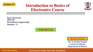
- 1. Introduction to Basics of Electronics Course Basic Electronics PHY-323 BS (Software Engineering) Semester : 1st Lecture # 1 Government College University, Faisalabad. Dr. M. Zeshan Yaqoob Lecturer in Physics Department of Physics, Resource Person Fall 2023-24 ©M. Zeshan Yaqoob
- 2. Government College University, Faisalabad. Lecture Outline 2 ©M. Zeshan Yaqoob ➢Course Outlines ➢Lecture Plan ➢Recommended Books ➢Evaluation Scheme ➢Interactive Session
- 3. Government College University, Faisalabad. 3 Course Outlines ©M. Zeshan Yaqoob Fundamentals of Semiconductor physics: Band theory, semiconductors (intrinsic and extrinsic), pn junction, pn junctions as a rectifier, clipper and clamper circuits, zener diode and voltage regulator, LED and LCD etc., Transistors: Bipolar Junction transistors, BJT biasing circuits, Q-point, BJT as a switch, BJT amplifiers, classes of amplifiers, power amplifiers, Metal oxide transistors, nMOS, pMOS and CMOS inverters circuits. Introduction to A/D and D/A conversion circuits
- 4. Government College University, Faisalabad. Lecture Plan Before Mid Term 4 ©M. Zeshan Yaqoob
- 5. Government College University, Faisalabad. 5 ©M. Zeshan Yaqoob • Fundamentals of Semiconductor physics: Band theory, semiconductors (intrinsic and extrinsic), • PN Junction, PN Junctions as a rectifier, clipper and clamper circuits, zener diode and voltage regulator, LED and LCD etc.,
- 6. Government College University, Faisalabad. Lecture Plan after Mid Term 6 ©M. Zeshan Yaqoob
- 7. Government College University, Faisalabad. 7 ©M. Zeshan Yaqoob • Transistors: Bipolar Junction transistors, BJT biasing circuits, Q-point, BJT as a switch, BJT amplifiers, • classes of amplifiers, power amplifiers, Metal oxide transistors, nMOS, pMOS and CMOS inverters circuits. Introduction to A/D and D/A conversion circuits
- 8. Government College University, Faisalabad. Lab Work 8 ©M. Zeshan Yaqoob
- 9. Government College University, Faisalabad. 9 ©M. Zeshan Yaqoob Physical Lab working
- 10. Government College University, Faisalabad. 10 ©M. Zeshan Yaqoob Virtual Lab working NI Multisim
- 11. Government College University, Faisalabad. Recommended Books 11 ©M. Zeshan Yaqoob 1.Basic Electronics, by Bernard Frob, 2.Electronic Devices, by Thomos Floyd Ed. 11th 3.Behzad Razavi,"Fundamentals of Microelectronics". 4.A.S. Sedraand K.C. Smith, "Microelectronic Circuits", Oxford University Press, Latest Edition.
- 12. Government College University, Faisalabad. 12 Evaluation Scheme ©M. Zeshan Yaqoob Step-I Assignment + Quiz Step-II Mid Term Exam Step-IV Final Term exam Step-III Practical Exam
- 13. Questions & Answers ❑ Zoom Meeting ❑ WhatsApp Group ❑ YouTube Comment Section Interactive session Government College University, Faisalabad.