
Recommended
More Related Content
What's hot
What's hot (20)
Similar to Sequential Circuits and Flip-Flops Explained
Similar to Sequential Circuits and Flip-Flops Explained (20)
Recently uploaded
Recently uploaded (20)
Sequential Circuits and Flip-Flops Explained
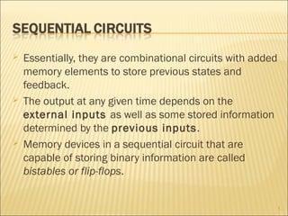
- 1. Essentially, they are combinational circuits with added memory elements to store previous states and feedback. The output at any given time depends on the external inputs as well as some stored information determined by the previous inputs. Memory devices in a sequential circuit that are capable of storing binary information are called bistables or flip-flops. 1
- 2. 1. SYNCHRONOUS Sequential Circuits These are systems whose behavior can be defined from the knowledge of its signals at discrete instances of time. Clocked sequential circuits, which change state at the clock pulse transition (therefore, a presence of master-clock generator). 2. ASYNCHRONOUS Sequential Circuits They depend upon the order in which its input signal changes and can be affected at any time. They are faster but are more complicated and are prone to malfunction. 2
- 3. a type of memory storage device that has two stable states (bistable) and is normally placed in a category separate from that of flip-flops. Latches are basically similar to flip -flops, the main difference between them is in the method used for changing their state. A latch can be implemented using 2 NOR gates or 2 NAND gates. 3
- 4. 4
- 5. It is a memory element or a binary cell which can store 1 bit of information indefinitely (as long as power is delivered to the circuit) until directed by an input signal to switch states. It has normally 2 outputs: Q - normal/true output and Q’ - complementary output. That is why, a flip-flop is also called a bistable. FOUR FLIP-FLOP FUNCTIONS 1. Reset 2. Set 3. Toggle 4. No change FOUR TYPES OF FLIP-FLOPS (A) S-R (Set-Reset) Flip-Flop (B) D (Data or gated D-latch) Flip-Flop (C) J-K Flip-Flop (D) T (Toggle) Flip-Flop 5
- 6. 6 Flip-flop is sensitive to pulse transition rather than pulse duration. a) Positive-Edge Triggering – would accept input at positive-going edge. b) Negative-Edge Triggering – would accept input at negative-going edge.
- 7. The S-R latch can be modified into an S-R flip- flop by providing an additional control input that determines when the state of the circuit is to be changed. Usually, this additional control is in the form of a clock pulse (CP). 7
- 8. One way to eliminate the undesirable condition of the indeterminate state in the S-R flip-flop is to ensure that inputs S and R are never equal to 1 at the same time. This is done in the D flip-flop. The D flip-flop receives the designation from its ability to hold data into its internal storage. 8
- 9. A J-K flip-flop is a refinement of the S-R flip-flop in that the indeterminate state of the S-R flip-flop is defined in the J-K flip- flop. Inputs J and K behave like S and R, to set and reset the flip-flop, respectively. J S (set) and K R (reset). 9
- 10. The T flip-flop is a single -input version of the J-K flip-flop. The designation T comes from the ability of the flip-flop to “toggle” or complement its state. 10
- 11. Example 1. Given the waveforms for the D input and the clock, determine the Q output waveform in the flip-flop starts out RESET. Assume that the positive edge-triggered flip- flop is given. 11
- 12. Example 2. The waveforms are applied to the J, K and clock inputs as indicated. Determine the Q output, assuming that the negative edge-triggered flip-flop is initially RESET. 12
- 13. Example 3. The waveforms shown below are to be applied to two different FFs: (a) positive edge triggered T FF (b) negative edge triggered T FF Assume that initial value of Q = 0, show the output waveform Q of the two FFs. 13
- 14. 14 [1] Thomas, Floyd L., Digital Fundamentals, 4th Edition, Macmillan Publishing Company, New York, 1990 [2] Mano, M. and Kime, C., Logic and Computer Design Fundamentals, 2nd Edition, Prentice Hall Int’l., N.J., 2001 [3] Mano, M., Digital Design, 2nd Edition, Prentice Hall, N.J, 1991 [4] Tocci, R. and Widmer, N., Digital Systems: Principles and Applications, 8th Edition, Prentice Hall Inc., N.J., 2001 [5] Swidlec Lecture Notes by Edzel Lapira, DLSU SWIDLEC LECTURE NOTES