08 lill ipv stuttgart
•
1 like•878 views

This document discusses laser processes that can be used to improve bifacial solar cells. It describes how selective laser doping can be used to dope emitter regions and bulk silicon to improve contacts and reduce shadowing on both sides of the solar cell. Laser transferred contacts are also discussed as a way to create fine line metallization patterns with reduced shadowing and contact resistance. Experimental results show that these laser processes can increase cell efficiency compared to standard diffusion processes. The laser techniques allow high selectivity and resolution and are well-suited for bifacial solar cell fabrication.

Recommended
More Related Content
What's hot
What's hot (20)
Similar to 08 lill ipv stuttgart
Similar to 08 lill ipv stuttgart (20)
More from Sandia National Laboratories: Energy & Climate: Renewables
More from Sandia National Laboratories: Energy & Climate: Renewables (20)
Recently uploaded
Recently uploaded (20)
08 lill ipv stuttgart
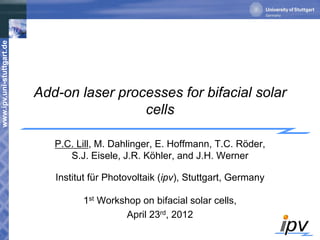
- 1. www.ipv.uni-stuttgart.de Add-on laser processes for bifacial solar cells P.C. Lill, M. Dahlinger, E. Hoffmann, T.C. Röder, S.J. Eisele, J.R. Köhler, and J.H. Werner Institut für Photovoltaik (ipv), Stuttgart, Germany 1st Workshop on bifacial solar cells, April 23rd, 2012
- 2. www.ipv.uni-stuttgart.de 2 Advantages high selectivity low temperature ambient air processes versatile
- 3. www.ipv.uni-stuttgart.de Laser processes for bifacial solar cells 3 ARC emitter screen printed metallization ARC screen printed metallization selectively laser doped bulk BSF locally increased doping improved contact improved contact reduced shadowing front and rear side laser transferred contacts
- 4. www.ipv.uni-stuttgart.de Laser doping process silicon substrate precursor layer laser doped region X Y 4 silicon substrate doping precursor liquid silicondoped region laser pulse
- 5. www.ipv.uni-stuttgart.de Benefits of laser doping highly flexible process applicable for front and rear side variety of doping precursors 5 industrially relevant only one additional process step commercially available tools selectively laser doped
- 6. www.ipv.uni-stuttgart.de Full area laser doped emitters 6*confirmed by ISE CalLab S. J. Eisele, T. C. Röder, J. R. Köhler, and J. H. Werner, Appl. Phys. Lett. 95, 133501 (2009). SiO2 - Al point contacts SiO2/ZnS/MgF2 Ti/Pd/Ag contacts p-type n+ laser doped emitter Cell structure 4 cm2 on polished Fz Voc [mV] Jsc [mA/cm2] FF [%] η [%] 677 35.2 79.1 18.9*
- 7. www.ipv.uni-stuttgart.de Cell structure 4 cm2 on polished Fz Voc [mV] Jsc [mA/cm2] FF [%] η [%] 677 35.2 79.1 18.9* 641 34.6 73.6 16.3 Full area laser doped emitters 6*confirmed by ISE CalLab S. J. Eisele, T. C. Röder, J. R. Köhler, and J. H. Werner, Appl. Phys. Lett. 95, 133501 (2009). SiO2 - Al point contacts SiO2/ZnS/MgF2 Ti/Pd/Ag contacts p-type n+ laser doped emitter SiO2 - Ti/Pd/Ag point contacts SiO2/SiNx Al contacts p+ laser doped emitter n-type furnace n+-BSF
- 8. www.ipv.uni-stuttgart.de 80 100 120 140 160 0 50 100 150 200 250 300 350 emittersaturation currentdensityJ0e [fA/cm²] emitter sheet resistance sh [/sq] High quality emitters 7 2.8 Ωcm, p-type Fz Phosphorus n+-emitter SiNx SiNx 3 Ωcm, n-type Fz Boron p+-emitter SiO2 SiO2
- 9. www.ipv.uni-stuttgart.de TexturingTexturing 8 Industrial concept – selective emitter Diffusion PSG removal Metallization Laser irradiation SiNx deposition Diffusion Laser irradiation PSG removal SiNx deposition Metallization Δη = +0.8% abs
- 10. www.ipv.uni-stuttgart.de Cell structure Rsh,emitter [Ω/sq] Voc [mV] Jsc [mA/cm2] FF [%] η [%] 60 623 36.5 76.9 17.5 80 625 37.1 76.1 17.7 Cell results 9 standard emitter
- 11. www.ipv.uni-stuttgart.de Cell structure Rsh,emitter [Ω/sq] Voc [mV] Jsc [mA/cm2] FF [%] η [%] 60 623 36.5 76.9 17.5 80 625 37.1 76.1 17.7 100 635 37.1 77.8 18.3 Cell results 9 selective emitter standard emitter
- 12. www.ipv.uni-stuttgart.de Laser processes for bifacial solar cells 10 ARC emitter screen printed metallization ARC screen printed metallization selectively laser doped bulk BSF locally increased doping improved contact improved contact reduced shadowing w < 30 µm laser transferred contacts
- 14. www.ipv.uni-stuttgart.de Benefits of LTC fine line metallization laser transferred contacts seed layer deposition contact emitter through ARC Ni, Al, Sb, Ti etc. low contact resistance Rc < 1 mcm2 @ 100 /sq 12 plating improve conductivity material: Ni/Cu good aspect ratio A 1:3 reduced shadowing w < 30 µm
- 15. www.ipv.uni-stuttgart.de Ni/Cu plating 13 LTC fine line solar cell LTC metallization Ni/Cu plating Texturing Diffusion P-glass removal SiNx deposition LTC metallization Rear contact SE laser doping η = 17.1%
- 16. www.ipv.uni-stuttgart.de LTC solar cells 14*confirmed by ISE CalLab LTC metal ACell [cm2] Voc [mV] Jsc [mA/cm2] FF [%] η [%] Ni 4 615 35.6 78.1 17.1* Ni with selective emitter 50 µm contact finger laser doped area
- 17. www.ipv.uni-stuttgart.de 50 µm contact finger LTC solar cells 14*confirmed by ISE CalLab LTC metal ACell [cm2] Voc [mV] Jsc [mA/cm2] FF [%] η [%] Ni 4 615 35.6 78.1 17.1* Sb 4 612 37.3 76.4 17.4 Ni with selective emitter Sb self doped contact 50 µm contact finger laser doped area
- 18. www.ipv.uni-stuttgart.de Conclusions laser processes high selectivity and spatial resolution low temperature processes laser doping n and p-type doping variety of precursors LTC fine line metallization reduce shadowing reduce contact resistance 15 selectively laser doped laser transferred contacts perfectly suited for bifacial solar cells!
- 19. www.ipv.uni-stuttgart.de 16 Thank you for your attention!