1. 4/3/2008
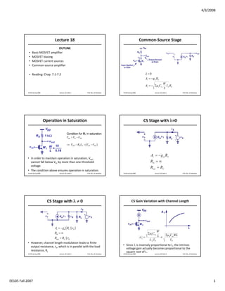
Lecture 18 Common‐Source Stage
OUTLINE
• Basic MOSFET amplifier
• MOSFET biasing
• MOSFET current sources
• Common‐source amplifier
Common source amplifier
• Reading: Chap. 7.1‐7.2 λ =0
Av = −g m RD
W
Av = − 2μnCox I D RD
L
EE105 Spring 2008 Lecture 18, Slide 1 Prof. Wu, UC Berkeley EE105 Spring 2008 Lecture 18, Slide 2 Prof. Wu, UC Berkeley
Operation in Saturation CS Stage with λ=0
Condition for M1 in saturation
Vout > Vin −VTH
⇒ VDD − RD I D > (VGS −VTH )
Av = − g m RL
• In order to maintain operation in saturation, Vout
cannot fall below Vin by more than one threshold Rin = ∞
voltage.
Rout = RL
• The condition above ensures operation in saturation.
EE105 Spring 2008 Lecture 18, Slide 3 Prof. Wu, UC Berkeley EE105 Spring 2008 Lecture 18, Slide 4 Prof. Wu, UC Berkeley
CS Stage with λ ≠ 0 CS Gain Variation with Channel Length
Av = −gm ( RL || rO )
Rin = ∞ W
2μnCox
Av = L ∝ 2μnCoxWL
Rout = RL || rO
λ ID ID
• However, channel length modulation leads to finite
output resistance, ro, which is in parallel with the load • Since λ is inversely proportional to L, the intrinsic
voltage gain actually becomes proportional to the
resistance, RL square root of L.
EE105 Spring 2008 Lecture 18, Slide 5 Prof. Wu, UC Berkeley EE105 Spring 2008 Lecture 18, Slide 6 Prof. Wu, UC Berkeley
EE105 Fall 2007 1
2. 4/3/2008
MOS Biasing Self‐Biased MOS Stage
R1
VDD = VGS + I D RS
R1 + R2
1 W
I D = μnCox (VGS − VTH )
2
2 L
2 unknows (VGS , I D ), 2 equations ⇒
I D RD +VGS + RS I D = VDD
1 W
I D = μnCox (VGS −VTH )
2
⎛ RV ⎞
VGS = − (V1 − VTH ) + V12 + 2V1 ⎜ 2 DD − VTH ⎟
⎝ R1 + R2 ⎠ 2 L
1
V1 =
W
μn Cox RS
L
• Voltage at X is determined by VDD, R1, and R2.
• The circuit above is analyzed by noting M1 is in
• VGS can be found using the equation above, and ID can be
found by using the NMOS current equation. saturation and no potential drop appears across RG.
EE105 Spring 2008 Lecture 18, Slide 7 Prof. Wu, UC Berkeley EE105 Spring 2008 Lecture 18, Slide 8 Prof. Wu, UC Berkeley
Current Sources CS Stage with Current‐Source Load
Av = − g m1 (rO1 || rO 2 )
Rout = rO1 || rO 2
• When in saturation region, a MOSFET behaves as a current source. • To alleviate the headroom problem, an active current‐source load
• NMOS draws current from a point to ground (sinks current), is used.
whereas PMOS draws current from VDD to a point (sources • This is advantageous because a current‐source has a high output
current). resistance and can tolerate a small voltage drop across it.
EE105 Spring 2008 Lecture 18, Slide 9 Prof. Wu, UC Berkeley EE105 Spring 2008 Lecture 18, Slide 10 Prof. Wu, UC Berkeley
PMOS CS Stage with NMOS as Load CS Stage with Diode‐Connected Load
Av = − g m 2 (rO1 || rO 2 )
⎛ 1 ⎞
Av = − g m1 ⎜ || rO 2 || rO1 ⎟
⎝ gm2 ⎠
1 (W / L )1
Av = − g m1 ⋅ =−
gm2 (W / L )2
• Similarly, with PMOS as input stage and NMOS as the
load, the voltage gain is the same as before. • Lower gain, but less dependent on process parameters.
EE105 Spring 2008 Lecture 18, Slide 11 Prof. Wu, UC Berkeley EE105 Spring 2008 Lecture 18, Slide 12 Prof. Wu, UC Berkeley
EE105 Fall 2007 2
3. 4/3/2008
CS Stage with Diode‐Connected PMOS Device CS Stage with Degeneration
⎛ 1 ⎞
Av = − g m 2 ⎜
⎜ g || ro1 || ro 2 ⎟
⎟
⎝ m1 ⎠
RD
Av = −
1
+ RS
gm
λ =0
• Note that PMOS circuit symbol is usually drawn with • Similar to bipolar counterpart, when a CS stage is degenerated,
the source on top of the drain. its gain, I/O impedances, and linearity change.
EE105 Spring 2008 Lecture 18, Slide 13 Prof. Wu, UC Berkeley EE105 Spring 2008 Lecture 18, Slide 14 Prof. Wu, UC Berkeley
Example of CS Stage with Degeneration CS Stage with Gate Resistance
VRG = 0
RD
Av = −
1 1
+
g m1 g m 2 • Since at low frequencies, the gate conducts no
current, gate resistance does not affect the gain or I/O
• A diode‐connected device degenerates a CS stage. impedances.
EE105 Spring 2008 Lecture 18, Slide 15 Prof. Wu, UC Berkeley EE105 Spring 2008 Lecture 18, Slide 16 Prof. Wu, UC Berkeley
Output Impedance of CS Stage with
Degeneration
Output Impedance Example (I)
rout ≈ gmrO RS + rO
⎛ 1 ⎞
Rout = rO1 ⎜1 + g m1 ⎟
• Similar to the bipolar counterpart, degeneration ⎝ gm2 ⎠
boosts output impedance. • When 1/gm is parallel with rO2, we often just consider 1/gm
EE105 Spring 2008 Lecture 18, Slide 17 Prof. Wu, UC Berkeley EE105 Spring 2008 Lecture 18, Slide 18 Prof. Wu, UC Berkeley
EE105 Fall 2007 3
4. 4/3/2008
Output Impedance Example (II) CS Core with Biasing
R1 || R2 − RD
Av = ⋅ , Av = − g m R D
RG + R1 || R2 1 + R
S
gm
Rout ≈ g m1rO1rO 2 + rO1
• Degeneration is used to stabilize bias point, and a bypass
• In this example, the impedance that degenerates the CS stage capacitor can be used to obtain a larger small‐signal voltage
is rO, instead of 1/gm in the previous example. gain at the frequency of interest.
EE105 Spring 2008 Lecture 18, Slide 19 Prof. Wu, UC Berkeley EE105 Spring 2008 Lecture 18, Slide 20 Prof. Wu, UC Berkeley
EE105 Fall 2007 4