
Recommended
More Related Content
What's hot
What's hot (20)
Similar to Impact of Coupling Coefficient on Coupled Line Coupler
Similar to Impact of Coupling Coefficient on Coupled Line Coupler (20)
More from rahulmonikasharma
More from rahulmonikasharma (20)
Recently uploaded
Recently uploaded (20)
Impact of Coupling Coefficient on Coupled Line Coupler
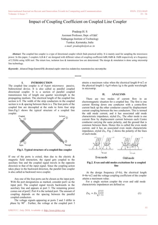
- 1. International Journal on Recent and Innovation Trends in Computing and Communication ISSN: 2321-8169 Volume: 6 Issue: 7 33 - 36 ______________________________________________________________________________________ 33 IJRITCC | July 2018, Available @ http://www.ijritcc.org _______________________________________________________________________________________ Impact of Coupling Coefficient on Coupled Line Coupler Pradeep.H. S Assistant Professor, Dept. of E&C Siddaganga Institute of Technology Tumkur, Karnataka, India e-mail: pradeephs@sit.ac.in Abstract- The coupled line coupler is a type of directional coupler which finds practical utility. It is mainly used for sampling the microwave power. In this paper, 3 couplers A,B & C are designed with different values of coupling coefficient 6dB,10dB & 18dB respectively at a frequency of 2.5GHz using ADS tool. The return loss, isolation loss & transmission loss are determined. The design & simulation is done using microstrip line technology. Keywords- AdvancedDesignSystem(ADS);directionalcoupler;returnloss;isolationloss;transmissionloss;microstripline. __________________________________________________*****_________________________________________________ I. INTRODUCTION The coupled line coupler is of 4-port microwave passive, bidirectional device. It is also called as parallel coupled directional coupler. It is a section of parallel coupled transmission line of length one quarter wavelength in the propagating medium. The electrical length of the coupled line section is θ. The width of the strip conductors in the coupled section is w & spacing between them is s. The four ports of the coupled line are decoupled at the ends to form four strip lines.Fig.1 shows the typical structure of a coupled line coupler. Fig.1. Typical structure of a coupled-line coupler If one of the ports is exited, then due to the electric & magnetic field interaction, the signal gets coupled to the auxiliary line and the coupled signal travels in the opposite direction to that of the input signal. Since the coupling action takes place in the backward direction, the parallel line coupler is also called as backward wave coupler. Any one of the four ports can be chosen as the input port. With the port designations as marked, consider port1 as the input port. The coupled signal travels backwards in the auxiliary line and appears at port 3. The remaining power comes out of port2. Port 4 is the isolated port. The amount of coupling depends on the spacing between the parallel coupled conductors. The voltage signals appearing at ports 2 and 3 differ in phase by 900 . Further, the voltage at the coupled port 3 attains a maximum value when the electrical length θ=π/2 or the physical length L=λg/4 where λg is the guide wavelength in microstrip. II. ANALYSIS There are two modes of current flow in an electromagnetic situation for a coupled line. The first is one current flowing down one conductor with a contra-flow current back up the other conductor caused by displacement current coupling between the two conductors. This is termed the odd mode current, and it has associated odd mode characteristic impedance, styled Zoo. The other mode is one current flow by displacement current between each Centre conductor carrying the same polarity, and the ground that is common between them. Hence this is called the even mode current, and it has an associated even mode characteristic impedance, styled Zoe. Fig. 2 shows the polarity of the lines of each mode. Fig.2. Even and odd modes excitations for a coupled line At the design frequency (f=fo), the electrical length θ=θo=π/2 and the voltage coupling coefficient of the coupler attains a maximum value. For a single section coupler the even and odd mode characteristic impedances are defined as: 𝑍𝑜𝑒 = 𝑍𝑜 1+𝐶𝑜 1−𝐶𝑜 (1)
- 2. International Journal on Recent and Innovation Trends in Computing and Communication ISSN: 2321-8169 Volume: 6 Issue: 7 33 - 36 ______________________________________________________________________________________ 34 IJRITCC | July 2018, Available @ http://www.ijritcc.org _______________________________________________________________________________________ 𝑍𝑜𝑜 = 𝑍𝑜 1−𝐶𝑜 1+𝐶𝑜 (2) Co is the mean coupling coefficient at the design frequency. The port impedance is Zo. The equations (1) & (2) form the design equations for this coupler. In the design of the coupler, the coupling coefficient and port impedance are specified. The values of Zoe & Zoo are calculated which in turn are used to determine the dimensions of the coupler. III. DESIGN The design parameters specification for coupled-line couplers are listed in the tables 1 and 2. These specifications are required to calculate the dimensions of the couplers can be. Fig. 3 shows the circuit configuration of the coupled line- coupler that will be designed. Fig.3. Coupled-line coupler circuit. The three couplers are designed for different values of coupling coefficient as shown in Table1. Table1.Coupler-line Coupling coefficient specification The specifications for the design of couplers are shown in Table2. Table 2. Design parameters specification. Parameters Specifications Characteristic impedance(in Ω) 50 Centre frequency (in GHz) 2.5 Substrate dielectric constant 4.5 Substrate thickness (in mm) 0.508 Loss tangent 0.0027 Metallisation/ Copper cladding (in um) 35 Planar Technology Microstrip line The design steps include determining the characteristic impedance for even mode and odd mode using the equations (1) and (2) respectively. The physical dimensions of the coupler are determined from Linecalc using ADS (Advanced Design System) tool. 1.Coupled-line coupler-A The dimensions & impedance values of coupler-A is shown in Table3. Table3: Dimensions of Coupler -A Coupler-A Parameter s Values Dimensions in mm Width (W) 0.136067 Length(L) 14.14350 Spacing(S) 0.014231 Characteristic Impedance in Ω Zoe 86.74 Zoo 28.82 The equivalent simulated circuit schematic and layout of coupled-line coupler A that obtained by using ADS tool are shown in fig. 4 and fig. 5. Fig.4: Circuit schematic of Coupler-A Fig.5: Layout of Coupler-A 2.Coupled-line coupler-B The dimensions & impedance values of coupler-B is shown in Table4. Table4: Dimensions of Coupler -B Coupler-B Parameters Values Dimensions in mm Width (W) 0.182452 Length(L) 14.14350 Spacing(S) 0.054063 Characteristic Impedance in Ω Zoe 69.37 Zoo 36.038 The equivalent simulated circuit schematic and layout of coupled-line coupler B that obtained by using ADS tool are shown in fig.6 and fig.7. Parallel line coupler Coupling coefficient C in dB Coupler-A 6 Coupler-B 10 Coupler-C 18
- 3. International Journal on Recent and Innovation Trends in Computing and Communication ISSN: 2321-8169 Volume: 6 Issue: 7 33 - 36 ______________________________________________________________________________________ 35 IJRITCC | July 2018, Available @ http://www.ijritcc.org _______________________________________________________________________________________ Fig.6: Circuit schematic of Coupler-B Fig.7: Layout of Coupler-B 3.Coupled-line coupler-C The dimensions & impedance values of coupler-C is shown in Table5. Table5: Dimensions of Coupler –C Coupler-C Parameters Values Dimensions in mm Width (W) 0.211943 Length(L) 14.14350 Spacing(S) 0.179522 Characteristic Impedance in Ω Zoe 56.75 Zoo 44.05 The equivalent simulated circuit schematic and layout of coupled-line coupler C that obtained by using ADS tool are shown in fig.8 and fig.9. Fig.8: Circuit schematic of Coupler-C Fig.9: Layout of Coupler-C IV. RESULTS There are different types of losses that occur in couplers which are defined in terms of scattering parameters namely 1.Return loss(dB) = −20𝑙𝑜𝑔 𝑆11 2.Transmission loss(dB) = −20𝑙𝑜𝑔 𝑆21 3.Isolation loss(dB) = −20𝑙𝑜𝑔 𝑆41 The variation of scattering parameters as a function of frequency is shown for different couplers A, B & C in Fig.10, Fig.11 & Fig.12 respectively. Fig.10: S-parameters variation as a function of frequency for coupler-A Fig.11: S-parameters variation as a function of frequency for coupler-B Fig.12: S-parameters variation as a function of frequency for coupler-C Table.6 shows the comparison of scattering parameters for three couplers. Better return loss (reflection at port 1) & isolation loss (between the ports 1 & 4) are achieved as the coupling factor increases. The coupler- C has better return loss & isolation loss compared to couplers A & B.
- 4. International Journal on Recent and Innovation Trends in Computing and Communication ISSN: 2321-8169 Volume: 6 Issue: 7 33 - 36 ______________________________________________________________________________________ 36 IJRITCC | July 2018, Available @ http://www.ijritcc.org _______________________________________________________________________________________ Table.6: Comparison of scattering parameters for three couplers. S- Parameters in dB Coupler- A (C=6dB) Coupler- B (C=10dB) Coupler- C (C=18dB) S11 -32.197 -38.895 -41.750 S21 -1.463 -0.598 -0.189 S31 -6.461 -10.269 -18.189 S41 -30.884 -39.438 -51.580 V. CONCLUSION In this paper, three coupled line couplers are designed and simulated using ADS tool using stripline planar technology. From the simulation results, it is observed that by varying the value of the coupling coefficient has an effect on the output power at ports at centre frequency 2.5GHz. The losses also varies with coupling factor. Also the dimensions of the coupler also changes with the coupling coefficient. The coupled line coupler C has better return loss & isolation loss compared to couplers A & B, but at the same time, the width & spacing between the conductors increases. On the other hand, coupler A has smaller dimensions with tolerable losses. REFERENCES [1] K. H. Yusof, N. Seman and M. H. Jamaluddin “ Design and Analysis of Wideband 3 and 6 dB Coupled-Line Coupler with different Grounding Techniques ’’ 2013 IEEE International RF and Microwave Conference (RFM 2013) December 09- 11,2013 –Penang Malaysia. [2] L. Chui, Q. Xue, “Investigation of a Wideband 900 Hybrid Coupler With an Arbitrary Coupling Level,” IEEE Trans. Microwave Theory & Tech., vol. 58, no. 4, pp. 1022 - 1029, April. 2010. [3] R. Mongia, I. Bahl, and P. Bhartia, RF and Microwave Coupled-Line Circuits. Boston, MA: Artech House, pp. 1– 21,1999. [4] Yongle Wu, Weinong Sun, Sai-Wing Leung, Yinliang Diao, Kwok-Hung Chan, and Yun-Ming Siu, Single-Layer Microstrip High-Directivity Coupled-Line Coupler With Tight Coupling” IEEE Transactions On Microwave Theory And Techniques, Vol. 61, No. 2, February 2013. [5] David M. Pozar, “Microwave Engineering”, fourth edition, John Wiley & Sons. Inc, 1998. [6] Leo G. Maloratsky, “Passive RF Microwave Integrated Circuits”. Elsevier Inc, 2004.