
Recommended
More Related Content
Similar to Carbon Nanomaterials and Allotropes
Similar to Carbon Nanomaterials and Allotropes (20)
More from ponjustin1
More from ponjustin1 (7)
Recently uploaded
Recently uploaded (20)
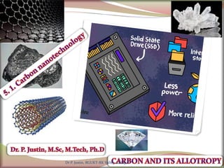
Carbon Nanomaterials and Allotropes
- 1. 1 Dr P. Justin, RGUKT-RK Valley, Kadapa.
- 2. Dr P. Justin, RGUKT-RK Valley, Kadapa. 2
- 3. 3 Carbon is the main element, and they exist in the form of ellipsoids, hollow spheres, and tubes. Graphite and diamond are allotropes of the most abundant element, carbon. It exists in all four dimensions of nanomaterials (i.e., 3D diamond and graphite, 2D graphite sheets, nanotubes in 1D, and fullerene in zero-dimension).. Dr P. Justin, RGUKT-RK Valley, Kadapa. The structural configuration and hybridization states of carbon strongly influence the electronic, physical, and chemical behavior of the nanomaterial. Carbon has six electrons, and its ground state configuration is 1s22s22p2. Carbon can be in sp, sp2, and sp3 hybridized state since it has a low energy gap among 2s, and 2p allows electron transition of its neighbouring carbon atom. The bond angle for sp, sp2 and sp3 hybridized carbon is 180°, 120° and 109.5°, respectively. And the corresponding geometry is Linear, Trigonal planar and Tetrahedral. In the case of sp hybridized carbon atoms, the covalent bonding with neighbour atoms at higher energy levels provides energy to compensate for this configuration, which is the same for sp2 and sp3 hybridization. The un hybrid p-orbitals consider π-bonding among themselves. The promising trigonometric sp3configuration exists for a diamond at high pressures and temperatures. With the decrease in the heat formation, the planar sp2 configuration adds up, thus forming a single-layered sheet structure with single π-bond and three-sigma covalent bonding.
- 4. 4 Dr P. Justin, RGUKT-RK Valley, Kadapa. Slight shear forces and chemical-physical separation induces weak interplanar forces among graphene sheets and induces slip-ups among them
- 5. 5 Most of the nanomaterials are unique, do not exist in nature and are truly “man-made” relatively recently. Sumio Iijima is a Japanese physicist and inventor who was the first to describe carbon nanotubes' formation clearly. Using an electron microscope, in 1991 he discovered carbon nanotubes (electron microscopic marvel), a fourth-allotrope carbon solid that became a focus of international attention.Carbon- based nanomaterials include fullerenes, carbon nanotubes, graphene and its derivatives, graphene oxide, nanodiamonds, and carbon-based quantum dots. Carbon is the fourth most prevalent element in the universe, and it exists in a variety of forms known as allotropes, depending on how carbon atoms are arranged. Polymorphic transition is a reversible transition of a solid crystalline phase at a certain temperature and pressure to another phase of the same chemical composition with a different crystal structure. Dr P. Justin, RGUKT-RK Valley, Kadapa.
- 6. 6 Dr P. Justin, RGUKT-RK Valley, Kadapa.
- 7. 7 Dr P. Justin, RGUKT-RK Valley, Kadapa.
- 8. 8 In materials science, the ability of a solid material (except elemental solids) to exist in more than one form or crystal structure is called polymorphism. Polymorphism is a form of isomerism. In materials science, the ability of a elemental solid material (not compound) to exist in more than one form or crystal structure is called allotropy. Polymorphic transition is a reversible transition of a solid crystalline phase at a certain temperature and pressure to another phase of the same chemical composition with a different crystal structure. 𝑸𝒖𝒂𝒓𝒕𝒛 (𝑺𝒊𝑶2) 870𝒐𝑪 𝑻𝒓𝒊𝒅𝒚𝒎𝒊𝒕𝒆(𝑺𝒊𝑶2 Dr P. Justin, RGUKT-RK Valley, Kadapa.
- 9. 9 Pure iron is magnetic and has a BCC crystal structure at room temperature, which changes to FCC (austenite, which is nonmagnetic ) iron at 912°C (1674°F). Dr P. Justin, RGUKT-RK Valley, Kadapa.
- 10. 10 Dr P. Justin, RGUKT-RK Valley, Kadapa.
- 11. 11 Dr P. Justin, RGUKT-RK Valley, Kadapa.
- 12. 12 In graphite, each carbon atom is attached to two other carbon atoms with single bond (sp2 hybrid, strong covalent) and third one with double bond delocalized (i.e., does not belong to a specific atom or bond i.e., free electron) in a regular hexagonal fashion. This hexagonal arrangement gives two dimensional sheets arranged parallel to each other (spacing is 0.335 nm) and linked via weak vander walls interaction. This arrangement and parallel sheet structure make graphite soft, good conductor of electricity because of free electrons from pi-bond and slippery to touch. In each layer is arranged in the honey comb lattice and it is highly anisotropic. In oxygen containing atmospheres, the graphite readily converted into carbon dioxide at temperatures of 700oC and above. It is diamagnetic. Dr P. Justin, RGUKT-RK Valley, Kadapa.
- 13. 13 Graphite and diamond have comparable free energies (=-3kJ/mol), yet forming diamond from graphite is far from easy. However, it’s the kinetic aspect (activation energy or Ea) of this process that screws this up ( higher activation energy or Ea) So compare to the small energy gap of the process, lots of energy is needed to overcome the Ea hill which is why you needs high pressure and temperature (12 Giga Pascal's and 1700K ) with precise control to turn graphite into diamond. To form diamond, the hexagonal rings in graphite first have to deform. Khaliullin and co (Ref: arxiv.org/abs/1101.1406) show that at low pressures, below 10GPa, the hexagonal rings in graphite tend to form the boat-shaped structure. When this happens, the graphite forms into a metastable allotrope of carbon called hexagonal diamond. Dr P. Justin, RGUKT-RK Valley, Kadapa.
- 14. 14 Dr P. Justin, RGUKT-RK Valley, Kadapa.
- 15. 15 1. J. Park, T. S. Sudarshan “Chemical Vapor Deposition (Surface Engineering Series, Vol 2)”, ASM International® Materials Park, 2001. 2. Jong-Hee Park, T. S. Sudarshan “Chemical Vapor Deposition (Surface Engineering Series, Vol 2)”, ASM International® Materials Park, 2001. 3. L. Murr, “ Industrial Materials Science and Engineering” Marcel Dekker Inc., 1984. 4. William D. Callister Jr., David G. Rethwisch, “Fundamentals of Materials Science and Engineering: An Integrated Approach”, 5th edition, Wiley, 2018. 5. From websites like google, wikipedia, researchgate,etc References Dr P. Justin, RGUKT-RK Valley, Kadapa.
- 16. 1 Dr P. Justin, RGUKT-RK Valley, Kadapa.
- 17. 2 As civilization progressed, natural diamonds diminished in the earth's crust due to exhausted mining, which led to much research on the artificial synthesis of diamonds. Scientists successfully synthesized crystalline diamonds in the 1950s using ultra-high pressure, requiring unique and expensive equipment. As a result, more research on the inexpensive and large-scale production technique of diamonds increased tremendously. At the beginning of the 1970s when researchers discovered that diamond crystals could be grown as thin coatings at low deposition pressures (102-103 Pa) from hydrocarbon gas or carbon vapour (gaseous phase)diamond by chemical vapour deposition (CVD). Dr P. Justin, RGUKT-RK Valley, Kadapa. Nanocrystalline diamond or Diamond-like carbon (DLC) was discovered accidentally during research on the vapour-phase synthesis of a diamond by Aisenberg et al. in 1971. From this accident discovery onwards, overwhelming interest has grown in generating and using high-quality diamond coatings over metallic and ceramic substrates for various mechanical, electronic, optical, and tribological applications. Properties that make diamond coatings very attractive for such applications include exceptionally high mechanical hardness, ultralow friction and wear coefficients, excellent thermal conductivity, minimum thermal expansion and excellent chemical inertness and high corrosion resistance. Combining these exceptional qualities in one material is scarce and makes it ideal for numerous industrial applications.
- 18. 3 Diamond is an allotrope of carbon in which the carbon atoms are arranged in a diamond cubic crystal lattice, and it is also the most popular gemstone. They are made of nearly 100% carbon atoms and are so durable that the only other mineral that can scratch a diamond's surface is another diamond. The diamond boasts the highest thermal conductivity and hardness of all naturally occurring materials. High electrical resistivity. In a cubic diamond structure, all atomic sites are occupied by two identical carbon atoms in the conventional fcc crystal lattice. In this structure, one of the sublattices is shifted along the body diagonal of the cubic cell by one-quarter (1/4) of the length of the diagonal i.e., an extra atom is placed at ¼a1 + ¼a2+ ¼a3 from each of the fcc atoms. This arrangement leads to the formation tetrahedral structure where four equal-distanced neighbouring carbon atoms (NNs) surround each carbon atom, as shown in the figure. The basic element of the structure is a tetrahedron where each carbon atom is at the centre, and its four NNs areat the corners of the cube (or vice versa). Dr P. Justin, RGUKT-RK Valley, Kadapa.
- 19. 4 Each atom forms four bonds with its NNs. Atoms in diamond-type crystals form covalent bonding. The bonding energy is associated with the shared valence electrons between atoms and depends on the relative orientation of atoms. Semiconductors such as diamond (C), silicon (Si), germanium and grey tin (α-Sn) crystallize in the diamond cubic structure. The atomic arrangement in the diamond structure helps explain its mechanical, chemical, and metallurgical properties. These semiconductor crystals can be cleaved along certain atomic planes to produce excellent planar surfaces, e.g., diamonds used in jewelry. Such surfaces are used as Fabry–Pérot reflectors in semiconductor lasers. Chemical reactions performed with such crystals, such as etching, often occur preferentially in certain directions. Dr P. Justin, RGUKT-RK Valley, Kadapa.
- 20. 5 Each carbon atom has undergone sp3 hybridization so that it bonds (tetrahedral) to four other carbons; these are extremely strong covalent bond with length 0.155 nm and bond angle 109,5o. It is a strong, rigid three- dimensional structure that results in an infinite network of atoms. Total number of atoms in diamond cubic structure is 8. This accounts for diamond's hardness, extraordinary strength and durability and gives diamond a higher density than graphite (3.514 grams per cubic centimeter). Since each electrons of C is included in single bond so there is no free electron available and hence diamond is bad conductor of electricity Dr P. Justin, RGUKT-RK Valley, Kadapa.
- 21. Dr P. Justin, RGUKT-RK Valley, Kadapa. 6
- 22. Dr P. Justin, RGUKT-RK Valley, Kadapa. 7 https://www.debeers.com/en-us/home ₹88,69,072.50 ₹3,60,000 ₹9,000
- 23. Dr P. Justin, RGUKT-RK Valley, Kadapa. 8
- 24. Dr P. Justin, RGUKT-RK Valley, Kadapa. 9
- 25. Dr P. Justin, RGUKT-RK Valley, Kadapa. 10 The methods for producing DLC by exposing a the base material to glow discharge plasma of a hydrocarbon gas like Acetylene (C2H2) or methane (CH4). The major methods for generating glow discharge in decompressed gas includes the DC discharge and RF discharge methods. Many of them apply the high-frequency power or a negative DC voltage to the base material, which is the cathode, and the counter anode is kept at the ground potential.
- 26. Dr P. Justin, RGUKT-RK Valley, Kadapa. 11
- 27. Dr P. Justin, RGUKT-RK Valley, Kadapa. 12
- 28. Dr P. Justin, RGUKT-RK Valley, Kadapa. 13
- 29. Dr P. Justin, RGUKT-RK Valley, Kadapa. 14
- 30. Dr P. Justin, RGUKT-RK Valley, Kadapa. 15
- 31. Dr P. Justin, RGUKT-RK Valley, Kadapa. 16
- 32. Dr P. Justin, RGUKT-RK Valley, Kadapa. 17 Dome coated with DLC for optical and tribological purposes A Co-alloy valve part from a producing oil well (30 mm diameter), coated on the right side with ta-C, in order to test for added resistance to chemical and abrasive degradation in the working environment. A Co-alloy valve part from a producing oil well (30 mm diameter), coated on the right side with ta-C, in order to test for added resistance to chemical and abrasive degradation in the working environment.
- 33. Dr P. Justin, RGUKT-RK Valley, Kadapa. 18
- 34. Dr P. Justin, RGUKT-RK Valley, Kadapa. 19
- 35. Dr P. Justin, RGUKT-RK Valley, Kadapa. 20 Any application exploiting diamond properties in a thin film configuration could profit from integrating nanocrystalline diamonds. This is especially apparent in passive applications such as heat spreading, tribology, optical coatings etc. Due to its extreme hardness, diamond has long been used for cutting, drilling, mining and milling everything from the hardest rock to the softest aluminium. Diamond-like films exhibit relatively good wear resistance, abrasive resistance, and sliding coefficient of friction. These properties help it find applications in the bearing industry (even for wind turbine shaft bearings) and in those machine components where relative sliding is involved. Bearings coated with these films will be silent in operation due to less friction. This also means that the life of the bearing can be increased, thereby reducing the running cost of the machine Improvement in Scratch resistance by a factor of 6 has been obtained for plastic lenses coated with these films.
- 36. Dr P. Justin, RGUKT-RK Valley, Kadapa. 21
- 37. Dr P. Justin, RGUKT-RK Valley, Kadapa. 22 There are an increasing number of applications that require a material with high thermal conductivity, as well as high strength and minimum weight. Aerospace applications include, jet engine and gear system, heat exchangers in hypersonic vehicles operating over a wide temperature range of 20-930°C, cooling fans in space power systems operating up to 780°C. The properties of these films like good surface hardness, excellent wear resistance, chemical inertness and environment durability can be put to good use in the automobiles industry. The development of diamond-like coating specifically for automotive polymers seems to offer great promise and could increase the use of low cost polymer material. When plastic is substituted for heavier material, the vehicle weight is reduced and this translates directly into energy saving through reduced fuel consumption.
- 38. Dr P. Justin, RGUKT-RK Valley, Kadapa. 23 Diamond has potential applications as human implant coatings because they fulfil the primary requisites for use in human implants: biocompatibility and chemical stability. Diamond coatings have been deposited on surgically implantable substrates such as ceramics used in dental implants, stainless steel, titanium and molybdenum used for prosthetic devices, etc.. Diamond coatings have been deposited on surgically implantable substrates such as ceramics used in dental implants, stainless steel, titanium and molybdenum used for prosthetic devices, etc.
- 39. Dr P. Justin, RGUKT-RK Valley, Kadapa. 24 The diamond films are used as dielectric layers for thermal management systems. In this case, the NCD film is coated on copper inserts used as heat transfer devices in multichip. For example, the high-performance multichip modules involve power density levels that are difficult to cope with using conventional packaging materials. Recently a composite CVD diamond-silicon heat spreader has been demonstrated to have superior properties at a production cost comparable to that of the traditional materials like AlN and CuW. Recently, NCD coating has been demonstrated to lead to an increase in the electron emission of molybdenum emitters. Boron doping leads to p type semiconducting diamond, and although n type doping has proved to be elusive, a number of prototype electronic devices have been demonstrated using NCD diamond, such as thermistors, field effect transistors, Schottkey diodes, field emission arrays. The highest thermal conductivity combined with the highest elastic constant make diamond useful in surface acoustic wave devices for high-frequency operations and telecommunication. Diamond based SAW the device has the edge over other materials since it can be operated at higher frequencies which means that more information can be transmitted.
- 40. Dr P. Justin, RGUKT-RK Valley, Kadapa. 25 Due to its transparency to a wide range of wavelengths from the infrared to the ultraviolet region and even x-rays combined together with low atomic number, radiation hardness and mechanical sturdiness, diamond is an ideal choice as a protective window material for lasers, X- ray sources, etc. These films are scratch/chemical resistant and block ultraviolet radiation. These properties, taken together, can revolutionize the spectacle and medical protective goggle industry. Improvement in scratch resistance by a factor of 6 has been obtained for plastic lenses coated with these films. The protective overcoat increases the life of many other potentially valuable coatings in different applications, for example, the soft Indium-Tin Oxide film used in photovoltaic applications, soft YBaCu2O3 superconducting thin films, provided the diamond-like overcoat does not alter or influence the basic properties of the underlying soft coating. NCD films with precise control over refractive index and thickness also have been deposited on silicon solar cells as antireflection coatings increasing in cell efficiency by 40% and on germanium windows as transparent protective coatings. The smooth and wear-resistant NCD coatings have been shown to provide excellent protection to discs for use as magnetic recording media without affecting the inherent properties of the magnetic material. The NCD coating on the recording head can prevent wear of the magnetic layer and subsequent data loss. The high film hardness and high chemical inertness makes NCD films more suitable as passivation layers for sensor devices as compared to other materials, such as Si3N4 and SiO2.
- 41. 26 1. J. Park, T. S. Sudarshan “Chemical Vapor Deposition (Surface Engineering Series, Vol 2)”, ASM International® Materials Park, 2001. 2. Jong-Hee Park, T. S. Sudarshan “Chemical Vapor Deposition (Surface Engineering Series, Vol 2)”, ASM International® Materials Park, 2001. 3. L. Murr, “ Industrial Materials Science and Engineering” Marcel Dekker Inc., 1984. 4. William D. Callister Jr., David G. Rethwisch, “Fundamentals of Materials Science and Engineering: An Integrated Approach”, 5th edition, Wiley, 2018. 5. From websites like google, wikipedia, researchgate,etc References Dr P. Justin, RGUKT-RK Valley, Kadapa.
- 42. 1 Dr P. Justin, RGUKT-RK Valley, Kadapa.
- 43. 2 Carbon nanotubes (CNTs) consist of a single sheet of graphite (i.e., graphene) rolled into a cylindrical tube and are chemically bonded with sp2 bonds-powerful form of molecular interaction. Each nanotube is a single molecule composed of millions of atoms; the length of this molecule is much greater (on the order of thousands of times greater) than its diameter. Multiple-walled carbon nanotubes (MWCNTs) consisting of concentric cylinders also exist.
- 44. 3 Dr P. Justin, RGUKT-RK Valley, Kadapa.
- 45. Dr P. Justin, RGUKT-RK Valley, Kadapa. 4 CNTs are synthesized by the thermal CVD method using hydrocarbon gas as a carbon source. In this method, a quartz tube is placed inside a furnace maintained at a high temperature (500– 900°C) and heated by an RF heater for a specified time. A crucible containing the substrate coated with catalyst nanoparticles is placed inside a quartz tube filled with inert gas. The experimental setup is shown below.
- 46. Dr P. Justin, RGUKT-RK Valley, Kadapa. 5 Zeolite (Sodium aluminium silicate) Types of CVD Name Heating Source Thermal- activated CVD IR radiation, RF heater, etc. Photo Assisted CVD Arc lamps, CO2 laser, Argon ion laser, Nd: YAG laser, etc. Plasma-assisted CVD microwave radiation, etc. Thermally Activated Chemical Vapour Deposition (CVD) Growth of Single-Walled Carbon Nanotubes (SWCNTs) Carbon Sources Hydrocarbon gases such as acetylene, ethylene, methane, etc. Substrate Substrates are materials on which the CNTS are grown—Zeolite, Silica, Silicon plate coated with iron particles, etc. Catalyst Iron, cobalt, nickel, molybdenum, iron- molybdenum alloys, etc. Heating Source RF Heater Conditions Temperature 500–900°C Inert gas Argon
- 47. 6 Dr P. Justin, RGUKT-RK Valley, Kadapa.
- 48. 7 Nanotubes are extremely strong and stiff and relatively ductile. The tensile strength of carbon nanotubes is approximately 100 times greater than that of steel of the same diameter i.e., one of the strongest known materials (tensile strengths range between 13 and 53 GPa)- Graphene is strongest. CNT is 100 times stronger than stainless steel and six times lighter. The first is the strength provided by the interlocking carbon-to-carbon covalent bonds. The second is the fact that each carbon nanotube is one large molecule (made-up of millions of atoms) Since each carbon atom has four electrons in the outer shell and only three are used to form covalent bonds, there is one remaining electron that is highly mobile (free electron) and available for electrical conduction. As a consequence, both CNT and graphene are highly conductive. Carbon nanotubes are very interesting materials for electrical engineering applications as they have all the characteristics of a perfect electrical conductor, very high conductivity, current carrying capacity, strength, and thermal conductivity, all combined with very low weight. The current-carrying capacity of CNT is 1000 times higher than that of copper. CNT can be metallic or semiconducting, depending on their diameter and chirality. In the semiconducting state they may be used for transistors and diodes. Furthermore, nanotubes are excellent electric field emitters. As such, they can be used for flat-screen displays (e.g., television screens and computer monitors).
- 49. 8 The current-carrying capacity of CNT is 1000 times higher than that of copper. CNT can be metallic or semiconducting, depending on their diameter and chirality. In the semiconducting state they may be used for transistors and diodes. Furthermore, nanotubes are excellent electric field emitters. As such, they can be used for flat-screen displays (e.g., television screens and computer monitors).
- 50. 9 Dr P. Justin, RGUKT-RK Valley, Kadapa.
- 51. 10 Dr P. Justin, RGUKT-RK Valley, Kadapa.
- 52. 11 Graphene, the newest member of the nanocarbons, is a single atomic layer of graphite, composed of hexagonally sp2 bonded carbon atoms. These bonds are extremely strong, yet flexible, which allows the sheets to bend. It is about 200 times stronger than steel it Can Stop a Speeding Bullet. The first graphene material was produced by peeling apart a piece of graphite, layer by layer using plastic adhesive tape until only a single layer of carbon remained.
- 53. 12 Two characteristics of graphene make it an exceptional material. First is the perfect order found in its sheets—no atomic defects such as vacancies exist; also, these sheets are extremely pure—only carbon atoms are present. The second characteristic relates to the nature of the unbonded electrons: at room temperature, they move much faster than conducting electrons in ordinary metals and semiconducting materials. In terms of its properties, graphene could be labeled the ultimate material. It is the strongest known material (~130 GPa), the best thermal conductor (~5000 W/m∙K), and has the lowest electrical resistivity (10−8 Ω∙m)—that is the best electrical conductor. Furthermore, it is transparent, chemically inert, and has a modulus of elasticity comparable to the other nanocarbons (~1 TPa).
- 54. 13
- 55. 14
- 56. 15
- 57. 16 1. Take 69 mL of 9:1 mixture of conc H2SO4/H3PO4 (62.1:6.9 mL) in a 250 mL beaker. (The bath was prepared by adding H2SO4 to the H3PO4 slowly and thoroughly mixing al most 60 min.) 2. To this add graphite flakes (3.00 g) followed by NaNO3 (1.5 g) very slowly with magnetic stirring. 3. Now cool the resulting mixture using an ice bath to <10 °C 4. After 60 min of stirring, add KMnO4 (9.00 g) very slowly and maintain the reaction temperature below 20 °C (~2h). 5. Heat the whole mixture ~35oC and stirred for 7 h. (The mixture turned green due to the formation of the oxidizing agent MnO3 +) 6. After 7 h the green color of MnO3 + was diminished, indicating that the oxidizing agent was consumed. 7. Now add additional KMnO4(9.00 g) to the above solutions and maintain the reaction mixture at~35oC for 12 h. 8. Add 120 mL of distilled water to the above reaction mixture and maintain the reaction mixture at~90oC for 30 min.
- 58. 17 13. Finally GO underwent purification with ethanol (2 times) and collect the GO from centrifuge tube by using ethanol and transfer to 250 mL beaker. 14. Measure the whole mixture and take exactly 1/10th of GO with ethanol into petty dishes. The obtained solid materials were kept in the oven at 50oC for five days & take the weight. 15. Remaining GO transfer to empty ethanol container and store in freezer for further applications. 9. The reaction was cooled to RT and poured onto ice (400 mL) with 30% H2O2 (6-12 mL or until the purple KMnO4 color disappeared). 10. Upon addition of the H2O2the mixture turned light-yellow. 11. After 20 min of swirling, the mixture underwent centrifugation, decanting and purified. 12. The graphite oxide was washed and centrifuged with 20% HCl (2 times, ~200 mL) and distilled water (minimum 3 times) sequentially until the pH level was 7.
- 59. 18
- 60. 19 A fullerene is an allotrope of carbon whose molecule consists of large number of carbon atoms connected to form both hexagonal (six-carbon atom) and pentagonal (five-carbon atom) geometrical configurations with single and double bonds so as to form a closed or partially closed mesh i.e., cuboid structure. Buckminsterfullerene is a type of C60 molecules fullerene consist of 20 hexagons and 12 pentagons, which are arrayed such that no two pentagons share a common side; the molecular surface thus exhibits the symmetry of a soccer ball (Truncated isohedron). Named in honor of R. Buckminster Fuller (1985), who invented the geodesic dome; each C60 is simply a molecular replica of such a dome. But, the smallest bucky ball cluster is C20. It is the unsaturated version of the dodecahedrane. The fullerenes that are larger in diameter than the nano tube and having walls of different thickness are mega tubes. Uses and potential applications of fullerenes include antioxidants in personal care products, biopharmaceuticals, catalysts, organic solar cells, long-life batteries, high- temperature superconductors, and molecular magnets.
- 61. 20
- 62. 21 1. J. Park, T. S. Sudarshan “Chemical Vapor Deposition (Surface Engineering Series, Vol 2)”, ASM International® Materials Park, 2001. 2. Jong-Hee Park, T. S. Sudarshan “Chemical Vapor Deposition (Surface Engineering Series, Vol 2)”, ASM International® Materials Park, 2001. 3. L. Murr, “ Industrial Materials Science and Engineering” Marcel Dekker Inc., 1984. 4. William D. Callister Jr., David G. Rethwisch, “Fundamentals of Materials Science and Engineering: An Integrated Approach”, 5th edition, Wiley, 2018. 5. From websites like google, wikipedia, researchgate,etc References Dr P. Justin, RGUKT-RK Valley, Kadapa.