Photocatalytic Mechanism Control and Study of Carrier Dynamics in CdS@C3N5 Core–Shell Nanowires

We present a potential solution to the problem of extraction of photogenerated holes from CdS nanocrystals and nanowires. The nanosheet form of C3N5 is a low-band-gap (Eg = 2.03 eV), azo-linked graphenic carbon nitride framework formed by the polymerization of melem hydrazine (MHP). C3N5 nanosheets were either wrapped around CdS nanorods (NRs) following the synthesis of pristine chalcogenide or intercalated among them by an in situ synthesis protocol to form two kinds of heterostructures, CdS-MHP and CdS-MHPINS, respectively. CdS-MHP improved the photocatalytic degradation rate of 4-nitrophenol by nearly an order of magnitude in comparison to bare CdS NRs. CdS-MHP also enhanced the sunlight-driven photocatalytic activity of bare CdS NWs for the decolorization of rhodamine B (RhB) by a remarkable 300% through the improved extraction and utilization of photogenerated holes due to surface passivation. More interestingly, CdS-MHP provided reaction pathway control over RhB degradation. In the absence of scavengers, CdS-MHP degraded RhB through the N-deethylation pathway. When either hole scavenger or electron scavenger was added to the RhB solution, the photocatalytic activity of CdS-MHP remained mostly unchanged, while the degradation mechanism shifted to the chromophore cleavage (cycloreversion) pathway. We investigated the optoelectronic properties of CdS-C3N5 heterojunctions using density functional theory (DFT) simulations, finite difference time domain (FDTD) simulations, time-resolved terahertz spectroscopy (TRTS), and photoconductivity measurements. TRTS indicated high carrier mobilities >450 cm2 V–1 s–1 and carrier relaxation times >60 ps for CdS-MHP, while CdS-MHPINS exhibited much lower mobilities <150 cm2 V–1 s–1 and short carrier relaxation times <20 ps. Hysteresis in the photoconductive J–V characteristics of CdS NWs disappeared in CdS-MHP, confirming surface passivation. Dispersion-corrected DFT simulations indicated a delocalized HOMO and a LUMO localized on C3N5 in CdS-MHP. C3N5, with its extended π-conjugation and low band gap, can function as a shuttle to extract carriers and excitons in nanostructured heterojunctions, and enhance performance in optoelectronic devices. Our results demonstrate how carrier dynamics in core–shell heterostructures can be manipulated to achieve control over the reaction mechanism in photocatalysis.

Recommended
Recommended
More Related Content
What's hot
What's hot (19)
Similar to Photocatalytic Mechanism Control and Study of Carrier Dynamics in CdS@C3N5 Core–Shell Nanowires
Similar to Photocatalytic Mechanism Control and Study of Carrier Dynamics in CdS@C3N5 Core–Shell Nanowires (20)
More from Pawan Kumar
More from Pawan Kumar (20)
Recently uploaded
Recently uploaded (20)
Photocatalytic Mechanism Control and Study of Carrier Dynamics in CdS@C3N5 Core–Shell Nanowires
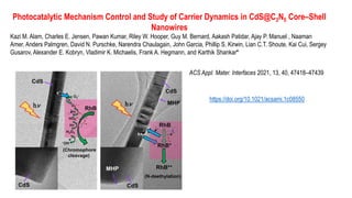
- 1. Photocatalytic Mechanism Control and Study of Carrier Dynamics in CdS@C3N5 Core–Shell Nanowires Kazi M. Alam, Charles E. Jensen, Pawan Kumar, Riley W. Hooper, Guy M. Bernard, Aakash Patidar, Ajay P. Manuel , Naaman Amer, Anders Palmgren, David N. Purschke, Narendra Chaulagain, John Garcia, Phillip S. Kirwin, Lian C.T. Shoute, Kai Cui, Sergey Gusarov, Alexander E. Kobryn, Vladimir K. Michaelis, Frank A. Hegmann, and Karthik Shankar* ACS Appl. Mater. Interfaces 2021, 13, 40, 47418–47439 https://doi.org/10.1021/acsami.1c08550
- 2. Figure 1. FESEM images of (a) pristine CdS nanowires (NWs), (b) CdS-MHP core–shell NWs formed by electrostatic wrapping of C3N5 around CdS NWs, and (c) CdS-MHPINS NWs formed by in situ growth of CdS/C3N5 heterostructures. The photographs of the materials are shown in the corresponding insets. HRTEM images showing (d, e) CdS crystal planes and a thin layer of surrounding C3N5 nanosheets in CdS-MHP and (f, g) CdS crystal planes and a thin layer of C3N5 nanosheets in CdS-MHPINS samples. EELS spectra of (h) CdS, (i) CdS-MHP, and (j) CdS-MHPINS showing energy loss peaks associated with constituent elements.
- 3. Figure 2. (a, c) X-ray diffractograms and DRS absorption spectra of pristine C3N5 bulk, pristine C3N5 nanosheet, pristine CdS nanowire, and heterojunctions of CdS with C3N5 nanosheets, respectively. (b, d) Raman spectra and steady-state photoluminescence spectra of pristine CdS nanowire and heterojunctions of CdS with C3N5 nanosheets, respectively.
- 4. Figure 3. FDTD electromagnetic simulation results for bare and C3N5 wrapped (2 nm thick) CdS nanowire of 200 nm length and 100 nm diameter. (a) Optical spectra (absorption, scattering, and extinction). (b–d) Electric field intensity profiles over xy, xz, and yz planes, respectively, for the bare CdS nanowire. (e–g) Electric field intensity profiles over xy, xz, and yz planes, respectively, for the C3N5 wrapped CdS nanowire. The electric field polarization direction is along the z axis in each and is indicated by yellow arrows. The nanowire is oriented vertically on an FTO substrate. The horizontal rectangle visible in the plots (c, d, f, and g) is the substrate.
- 5. Figure 4. (a) XPS elemental survey scan of CdS (black), C3N5 bulk (wine), C3N5 NS (cyan), CdS-MHP (red), and CdS-MHPINS (blue). HR- XPS spectra of (b) CdS, CdS-MHP, and CdS-MHPINS in the Cd 3d region; (c) CdS, CdS-MHP, and CdS-MHPINS in the S 2p region; (d) C3N5 bulk, C3N5 NS, CdS-MHP, and CdS-MHPINS in the C 1s region, (e) C3N5 bulk, C3N5 NS, CdS-MHP, and CdS-MHPINS in the N 1s region; and (f) CdS, CdS-MHP, and CdS-MHPINS in the O 1s region.
- 6. Figure 5. (a) 113Cd magic-angle spinning (MAS) Bloch decay NMR spectra of pristine CdS (top), CdS-MHP (middle), and CdS-MHPINS (bottom). (b) 113Cd cross-polarization magic-angle spinning (CPMAS) NMR spectra of pristine CdS (top), CdS-MHP (middle), and CdS- MHPINS (bottom). (c) 13C CPMAS NMR spectra of pristine C3N5 (top), CdS-MHP (middle), and CdS-MHPINS (bottom).
- 7. Figure 6. (a) −ΔE/Eref for CdS (black), CdS-MHP (red), and CdS-MHPINS (blue). The dark gray curves indicate biexponential fits to the data. Dashed vertical lines indicate times at which photoconductivity spectra were measured. The green line corresponds to tpp = 14 ps, while the magenta line indicates tpp = 154 ps after the onset of −ΔE/Eref. The fluence is 400 μJ/cm2 for all measurements, with a center wavelength of 410 nm and 100 fs duration. (b) Real (square) and imaginary (circle) photoconductivity spectra for the bare CdS nanowire sample taken at tpp = 14 ps (filled) and tpp = 154 ps (hollow). Real (solid line) and imaginary (dashed line) parts of the Drude–Smith model are shown as lines. (c) Same as (b), but for CdS-MHP. (d) Same as (b), but for CdS-MHPINS.
- 8. Figure 7. Photocatalytic test by RhB degradation experiment for pristine CdS, CdS-MHP, and CdS-MHPINS samples. (a) RhB degradation efficiency in the absence of any scavenger. (b) Comparative efficiencies for three photocatalysts in the absence of any scavenger and in the presence of electron and hole scavengers. Proposed photocatalytic mechanisms for (c) pristine CdS and (d) CdS-C3N5 composites.
- 9. Figure 8. Photocatalytic degradation experiments under AM1.5 G 1 sun simulated sunlight using 4-nitrophenol. (a) UV–vis absorption spectrum of bare 4-nitrophenol. Gradual evolution of UV–vis absorption spectra in the dark and under illumination for (b) pristine CdS, (c) CdS-MHP, and (d) CdS-MHPINS samples.
- 10. Figure 9. Side view of DFT optimized structures showing spatial distributions of molecular orbitals (HOMO–LUMO plots) for heterojunctions composed of two different CdS planes and single-layer C3N5. (a) Configuration I for CdS (100) plane and single-layer C3N5, (b) configuration II for CdS (100) plane and single-layer C3N5, (c) configuration I for CdS (110) plane and single-layer C3N5, and (d) configuration II for CdS (110) plane and single-layer C3N5. Cyan and magenta colors are for HOMO and LUMO surfaces, respectively. Cd, S, C, and N atoms are in red, yellow, gray, and blue colors, respectively.
- 11. Figure 10. Projected density of states (PDOS) of selected atoms for two different pristine CdS planes and their heterojunctions with single-layer C3N5. (a) Pristine CdS (100) plane, (b) configuration I for CdS (100) plane and single-layer C3N5, (c) configuration II for CdS (100) plane and single-layer C3N5, (d) pristine CdS (110) plane, (e) configuration I for CdS (110) plane and single-layer C3N5, and (f) configuration II for CdS (110) plane and single-layer C3N5. Cd, S, C, and N atoms are in wine, yellow, gray, and blue colors, respectively.