ADC - Types (Analog to Digital Converter)
•Download as PPTX, PDF•
1 like•754 views

ADC - Types (Analog to Digital Converter)

Recommended
More Related Content
What's hot
What's hot (20)
Similar to ADC - Types (Analog to Digital Converter)
Similar to ADC - Types (Analog to Digital Converter) (20)
More from National Engineering College
More from National Engineering College (20)
Recently uploaded
Recently uploaded (20)
ADC - Types (Analog to Digital Converter)
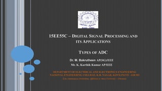
- 1. 15EE55C – DIGITAL SIGNAL PROCESSING AND ITS APPLICATIONS TYPES OF ADC Dr. M. Bakrutheen AP(SG)/EEE Mr. K. Karthik Kumar AP/EEE DEPARTMENT OF ELECTRICAL AND ELECTRONICS ENGINEERING NATIONAL ENGINEERING COLLEGE, K.R. NAGAR, KOVILPATTI – 628 503 (An Autonomous Institution, Affiliated to Anna University – Chennai)
- 2. INTRODUCTION An Analog to Digital Converter (ADC) takes an analog input signal and converts the input, through a mathematical function, into a digital output signal. While there are many ways of implementing an ADC, there are three conceptual steps that occur. The signal is sampled. The sampled signal is quantized. The quantized signal is digitally coded.
- 3. SAMPLING By, sampling we turn a continuous-time function which may take on infinitely many values at different times into a discretized function that may take on infinitely many values at different discrete indices. Sampling generally is done with a Sample-And-Hold circuit (simple experiments can be done using a capacitor and switch). To be able to reconstruct the signal we must consider the Sampling Theorem which says that a sampling frequency twice the highest frequency we're expecting is needed. In a simple way sampling can be defined as the process of taking samples from the continuous time function x(t) and for the signal to reconstruct we must consider the sampling theorem which states that the sampling frequency must be always greater than or equal to twice the highest frequency.
- 4. QUANTIZATION Quantization is the process of taking a continuous voltage signal and mapping it to a discrete number of voltage levels. The number of voltage levels affects the quantization noise that occurs. Since digital computers are binary in nature, the number of quantization levels is usually a power of 2, i.e., N= 2n, where n is the number of quantization bits. The signal may be amplified or attenuated before going into the ADC, so that the maximum and minimum voltage levels give the best compromise between resolution of the signal levels and minimization of clipping.
- 5. ENCODING Encoding is the process of converting the quantized signals into a digital representation. This encoding is performed by giving each quantization level a unique label. For instance, if four bits are used, the lowest level may be (in binary) 0000, and the next highest level 0001, etc.
- 6. TYPES Dual Slope A/D Converter Successive Approximation A/D Converter Flash A/D Converter Delta-Sigma A/D Converter Other: Voltage-to-frequency, staircase ramp or single slope, charge balancing or redistribution, switched capacitor, tracking, and synchro or resolver
- 8. DUAL SLOPE ADC Fundamental components: Integrator Electronically Controlled Switches Counter Clock Control Logic Comparator
- 9. DUAL SLOPE ADC - FUNCTIONING A dual-slope ADC (DS-ADC) integrates an unknown input voltage (VIN) for a fixed amount of time (TINT), then "de-integrates" (TDEINT) using a known reference voltage (VREF) for a variable amount of time. The key advantage of this architecture over the single-slope is that the final conversion result is insensitive to errors in the component values. That is, any error introduced by a component value during the integrate cycle will be cancelled out during the de-integrate phase.
- 10. DUAL SLOPE ADC - FUNCTIONING At t<0 S1 is set to ground, S2 is closed, and counter=0. At t=0 a conversion begins and S2 is open, and S1 is set so the input to the integrator is Vin. S1 is held for TINT which is a constant predetermined time interval. When S1 is set the counter begins to count clock pulses, the counter resets to zero after TINT Vout of integrator at t=TINT is VINTINT/RC is linearly proportional to VIN At t=TINT S1 is set so -Vref is the input to the integrator which has the voltage VINTINT/RC stored in it. The integrator voltage then drops linearly with a slope -Vref/RC. A comparator is used to determine when the output voltage of the integrator crosses zero When it is zero the digitized output value is the state of the counter.
- 11. DUAL SLOPE ADC – PROS AND CONS PROS Conversion result is insensitive to errors in the component values. Fewer adverse affects from “noise” High Accuracy CONS Slow Accuracy is dependent on the use of precision external components Cost
- 12. FLASH ADC
- 13. FLASH ADC Fundamental Components (For N bit Flash A/D): 2N-1 Comparators 2N Resistors Control Logic
- 14. FLASH ADC – FUNCTIONING Uses the 2N resistors to form a ladder voltage divider, which divides the reference voltage into 2N equal intervals. Uses the 2N-1 comparators to determine in which of these 2N voltage intervals the input voltage Vin lies. The Combinational logic then translates the information provided by the output of the comparators This ADC does not require a clock so the conversion time is essentially set by the settling time of the comparators and the propagation time of the combinational logic.
- 15. FLASH ADC – PROS AND CONS PROS Very Fast (Fastest) Very simple operational theory Speed is only limited by gate and comparator propagation delay CONS Expensive Prone to produce glitches in the output Each additional bit of resolution requires twice the comparators
- 17. SUCCESSIVE APPROXIMATION ADC Uses a n-bit DAC to compare DAC and original analog results. Uses Successive Approximation Register (SAR) supplies an approximate digital code to DAC of Vin. Comparison changes digital output to bring it closer to the input value. Uses Closed-Loop Feedback Conversion
- 18. SUCCESSIVE APPROXIMATION ADC – FUNCTIONING
- 19. SUCCESSIVE APPROXIMATION ADC – FUNCTIONING
- 20. SUCCESSIVE APPROXIMATION ADC – PROS AND CONS PROS Capable of high speed and reliable Medium accuracy compared to other ADC types Good tradeoff between speed and cost Capable of outputting the binary number in serial (one bit at a time) format CONS Higher resolution successive approximation ADC’s will be slower Speed limited to approx. 5MSPS
- 21. SIGMA – DELTA ADC
- 22. SIGMA – DELTA ADC Main Components Resistors Capacitor Comparators Control Logic
- 23. SIGMA – DELTA ADC – FUNCTIONING Input is over sampled, and goes to integrator. The integration is then compared to ground. Iterates and produces a serial bit stream Output is a serial bit stream with # of 1’s proportional to Vin With this arrangement the sigma-delta modulator automatically adjusts its output to ensure that the average error at the quantizer output is zero. The integrator value is the sum of all past values of the error, so whenever there is a non-zero error value the integrator value just keeps building until the error is once again forced to zero.
- 24. SIGMA – DELTA ADC – PROS AND CONS PROS High Resolution No need for precision components CONS Slow due to over sampling Only good for low bandwidth