Ig3314081417
•
0 likes•451 views

International Journal of Engineering Research and Applications (IJERA) is an open access online peer reviewed international journal that publishes research and review articles in the fields of Computer Science, Neural Networks, Electrical Engineering, Software Engineering, Information Technology, Mechanical Engineering, Chemical Engineering, Plastic Engineering, Food Technology, Textile Engineering, Nano Technology & science, Power Electronics, Electronics & Communication Engineering, Computational mathematics, Image processing, Civil Engineering, Structural Engineering, Environmental Engineering, VLSI Testing & Low Power VLSI Design etc.

Recommended
Recommended
More Related Content
What's hot
What's hot (16)
Viewers also liked
Similar to Ig3314081417
Similar to Ig3314081417 (20)
Recently uploaded
Recently uploaded (20)
Ig3314081417
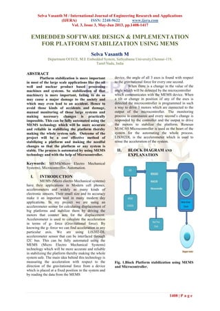
- 1. Selva Vasanth M / International Journal of Engineering Research and Applications (IJERA) ISSN: 2248-9622 www.ijera.com Vol. 3, Issue 3, May-Jun 2013, pp.1408-1417 1408 | P a g e EMBEDDED SOFTWARE DESIGN & IMPLEMENTATION FOR PLATFORM STABILIZATION USING MEMS Selva Vasanth M Department Of ECE, M.E Embedded System, Sathyabama University,Chennai-119, Tamil Nadu, India ABSTRACT Platform stabilization is more important in most of the large scale applications like the oil well and nuclear product based processing machines and systems. So stabilization of that machinery is more important, failing to do so may cause a major damage to the society and which may even lead to an accident. Hence to avoid those kinds of accidents and damage, manual monitoring of those large systems and making necessary changes is practically impossible. This can be fully automated using the MEMS technology which will be more accurate and reliable in stabilizing the platform thereby making the whole system safe. Outcome of the project will be a cost effective method of stabilizing a platform and making the needful changes so that the platform or any system is stable. The process is automated by using MEMS technology and with the help of Microcontroller. Keywords: MEMS(Micro Electro Mechanical Systems), Microcontroller, Automation. I. INTRODUCTION MEMS (Micro electro Mechanical systems) have their applications in Modern cell phones, accelerometers and widely as many kinds of electronic sensors. Their small size and its accuracy make it an important tool in many modern day applications. In my project we are using an accelerometer sensor for calculating displacement of big platforms and stabilize them by driving the motors that counter acts for the displacement. Accelerometer is used to calculate the acceleration in terms of g- force (Gravitational force). By knowing the g- force we can find acceleration in any particular axis. We are using LIS302-DL accelerometer sensor that can be interfaced through I2C bus. This can be fully automated using the MEMS (Micro Electro Mechanical Systems) technology which will be more accurate and reliable in stabilizing the platform thereby making the whole system safe. The main idea behind this technology is measuring the acceleration with respect to the direction of the gravitational force from a device which is placed at a fixed position in the system and by reading the data from the MEMS device, the angle of all 3 axes is found with respect to the gravitational force for every one second. When there is a change in the value of the angle which will be detected by the microcontroller which communicates with the MEMS device. When a tilt or change in position of any of the axes is detected the microcontroller is programmed in such a way to drive 3 motors which are connected to the output of the microcontroller. The monitoring process is continuous and every second’s change is responded by the controller and the output to drive the motors to stabilize the platform. Renesas M16C/65 Microcontroller is used as the heart of the system for the automating the whole process. LIS302DL is the accelerometer which is used to sense the acceleration of the system. II. BLOCK DIAGRAM AND EXPLANATION Fig. 1.Block Platform stabilization using MEMS and Microcontroller.
- 2. Selva Vasanth M / International Journal of Engineering Research and Applications (IJERA) ISSN: 2248-9622 www.ijera.com Vol. 3, Issue 3, May-Jun 2013, pp.1408-1417 1409 | P a g e Fig. 2. Graphical representation of the MEMS device which obeys at the rate of 2.5V and their output modulation (proposed by ST-Micro Systems (LIS302DL)). Fig.1 illustrates that the MEMS device which is just mean time connected with the Analogy to Digital Converter for more accuracy and this is fed in to the controller for processing. In this mean time the MEMS device which illustrates that it produces the reading in the range of 0-255 readings in a time scale based on the value of sensory production in all the X, Y and Z-axis slotted in the Fig.2. They are capable of producing the output sequentially through the I2C communication network. And the incoming values are stored in the buffer calculated and processed in the meantime and also in a regular time scale. Whenever there is a request from the controller the MEMS device have to initialize and produces the output through the I2C bus. And the value change remains periodically according to their state if there is any deflection found in that value’s the controller gets alerted and to drive the motor with the help of motor driver circuits. Here in this project proposal can be made with the help of simulation instead of the motor driver and control. III. HARDWARE DESCRIPTION Micro Electro Mechanical Systems (MEMS) Accelerometer (LIS302DL): The LIS302DL is an ultra-compact low- power three axes linear accelerometer. It includes a sensing element and an IC interface able to provide the measured acceleration to the external world through I2C/SPI serial interface. The sensing element, capable of detecting the 17 acceleration, is manufactured using a dedicated process developed by ST to produce inertial sensors and actuators in silicon. The IC interface is manufactured using a CMOS process that allows designing a dedicated circuit which is trimmed to better match the sensing element characteristics. The LIS302DL has dynamically user selectable full scales of ± 2g/± 8g and it is capable of measuring accelerations with an output data rate of 100 Hz or 400 Hz.A self-test capability allows the user to check the functioning of the sensor in the final application. The device may be configured to generate inertial wake-up/free-fall interrupt signals when a programmable acceleration threshold is crossed at least in one of the three axes. Thresholds and timing of interrupt generators are programmable by the user. The LIS302DL is available in plastic Thin Land Grid Array package (TLGA) and it is guaranteed to operate over an extended temperature range from -40 °C to +85 °C. The LIS302DL belongs to a family of products suitable for a variety of applications: Free-fall detection, Motion activated functions, gaming and virtual reality input devices, Vibration monitoring and compensation Features The LIS302DL have many important and useful features. Features of the MEMS IC LIS302DL are listed below: 1.8 V compatible IOs 8g dynamically selectable full Scale. -test Block Diagram The LIS302DL MEMS architecture includes Multiplexer, Analog to Digital Converter and Control unit. The input for the MEMS is taken from the movement of the object in which it is mounted. And the output is given to the master device by using I2C interface or SPI interface. The Block Diagram of the LIS302DL in Figure .3 as follows Fig. 3. Block Diagram of LIS302Dl proposed by ST Microsystems.
- 3. Selva Vasanth M / International Journal of Engineering Research and Applications (IJERA) ISSN: 2248-9622 www.ijera.com Vol. 3, Issue 3, May-Jun 2013, pp.1408-1417 1410 | P a g e RENESAS M16/C65 MICROCONTROLLER Features The M16C/65 Group microcomputer (MCU) incorporates the M16C/60 Series CPU core and flash memory, employing sophisticated instructions for a high level of efficiency. This MCU has 1 Mbyte of address space (expandable to 4 Mbytes), and it is capable of executing instructions at high speed. In addition, the CPU core boasts a multiplier for high-speed operation processing. Power consumption is low, and the M16C/65 Group supports operating modes that allow additional power control. The MCU also uses an anti-noise configuration to reduce emissions of electromagnetic noise and is designed to withstand electromagnetic interference (EMI). By integrating many of the peripheral functions, including the multifunction timer and serial interface, the number of system components has been reduced. Block Diagram Fig .4 The Block Diagram of the 100 pin M16C/65 proposed by RENUSAS. The M16C/65 Group includes 128-pin, 100-pin, and 80-pin packages. In this project we use 100 pin IC package. The Block Diagram of the 100 pin M16C/65 is shown in Figure 4. Fig .5 The Pin Assignment of the 100 pin M16C/65 (RENUSAS) I2C INITIALIZATION I2C Introduction I2C (Inter-Integrated Circuit) generically referred to as "two-wire interface" is a multi-master serial single-ended computer bus invented by Philips that is used to attach low-speed peripherals to a motherboard, embedded system, cellphone, or other electronic device. In my project I used to Operations I2C uses only two bidirectional open-drain lines, Serial Data Line (SDA) and Serial Clock (SCL), pulled up with resistors. Typical voltages used are +5 V or +3.3 V although systems with other voltages are permitted. The I2C reference design has a 7-bit address space with 16 reserved addresses, so a maximum of 112 nodes can communicate on the same bus. Common I2C bus speeds are the 100 kbit/s standard mode and the 10 kbit/s low-speed mode, but arbitrarily low clock frequencies are also allowed. Recent revisions of I2C can host more nodes and run at faster speeds (400 kbit/s Fast mode, 1 Mbit/sFast mode plus or Fm+, and 3.4 Mbit/s High Speed mode). These speeds are more widely used on embedded systems than on PCs. There are also other features, such as 16-bit addressing.Note that the bit rates quoted are for the transactions between master and slave without clock stretching or other hardware overhead. Protocol overheads include a slave address and perhaps a register address within the slave device as well as per-byte ACK/NACK bits. So the actual transfer rate of user data is lower than those peak bit rates alone would imply. For example, if each interaction with a slave inefficiently allows only 1 byte of data to be transferred, the data rate
- 4. Selva Vasanth M / International Journal of Engineering Research and Applications (IJERA) ISSN: 2248-9622 www.ijera.com Vol. 3, Issue 3, May-Jun 2013, pp.1408-1417 1411 | P a g e will be less than half the peak bit rate. The maximum number of nodes is limited by the address space, and also by the total bus capacitance of 400 pF, which restricts practical communication distances to a few meters. Message Protocols I2C defines three basic types of messages, each of which begins with a START and ends with a STOP: slave; slave; least two reads and/or writes to one or more slaves. In a combined message, each read or write begins with a START and the slave address. After the first START, these are also called repeated START bits; repeated START bits are not preceded by STOP bits, which is how slaves know the next transfer is part of the same message. Any given slave will only respond to particular messages, as defined by its product documentation.Pure I2C systems support arbitrary message structures. SMBus is restricted to nine of those structures, such as read word N and write word N, involving a single slave. PMBus extends SMBus with a Group protocol, allowing multiple such SMBus transactions to be sent in one combined message. The terminating STOP indicates when those grouped actions should take effect. For example, one PMBus operation might reconfigure three power supplies (using three different I2C slave addresses), and their new configurations would take effect at the same time: when they receive that STOP. In practice, most slaves adopt request/response control models, where one or more bytes following a write command are treated as a command or address. Those bytes determine how subsequent written bytes are treated and/or how the slave responds on subsequent reads. Most SMBus operations involve single byte commands. A sample schematic with one master (a microcontroller), three slave nodes (an ADC, a DAC, and a microcontroller), and pull-up resistors (Rp) is shown in Fig.6 Fig.6 A sample schematic of I2C Connection Timing Diagram Data transfer is initiated with the START bit (S) when SDA is pulled low while SCL stays high. Then, SDA sets the transferred bit while SCL is low (blue) and the data is sampled (received) when SCL rises (green). When the transfer is complete, a STOP bit (P) is sent by releasing the data line to allow it to be pulled up while SCL is constantly high. The timing diagram of I2C Bus is given in Figure 7 Fig.7 The timing diagram of I2C Bus. I2C Operations in MEMS The transaction on the bus is started through a START (ST) signal. A START condition is defined as a HIGH to LOW transition on the data line while the SCL line is held HIGH. After this has been transmitted by the Master, the bus is considered busy. The next byte of data transmitted after the start condition contains the address of the slave in the first 7 bits and the eighth bit tells whether the Master is receiving data from the slave or transmitting data to the slave. When an address is sent, each device in the system compares the first seven bits after a start condition with its address. If they match, the device considers itself addressed by the Master. Table .1 SAD+Read/Write patterns The Slave ADdress (SAD) associated to the LIS302DL is 001110xb. SDO pad can be used to modify less significant bit of the device address. If SDO pad is connected to voltage supply LSb is ‘1’ (address 0011101b) else if SDO pad is connected to ground LSb value is ‘0’ (address 0011100b). This solution permits to connect and address two different accelerometers to the same I2C lines. How the SAD+Read/Write bit pattern is composed, listing all the possible configurations are explains in Talbe 3.1 Data transfer with acknowledge is mandatory. The transmitter must release the SDA line during the acknowledge pulse. The receiver must then pull the data line LOW so that it remains stable low during the HIGH period of the acknowledge clock pulse. A
- 5. Selva Vasanth M / International Journal of Engineering Research and Applications (IJERA) ISSN: 2248-9622 www.ijera.com Vol. 3, Issue 3, May-Jun 2013, pp.1408-1417 1412 | P a g e receiver which has been addressed is obliged to generate an acknowledge signal after each byte of data has been received. The I2C embedded inside the LIS302DL behaves like a slave device and the following protocol must be adhered to. After the start condition (ST) a salve address is sent, once a slave acknowledge (SAK) has been returned, a 8-bit sub- address will be transmitted: the 7 LSb represent the actual register address while the MSB enables address auto increment. If the MSb of the SUB field is 1, the SUB (register address) will be automatically incremented to allow multiple data read/write. The slave address is completed with a Read/Write bit. If the bit was ‘1’ (Read), a repeated START (SR) condition will have to be issued after the two sub- address bytes; if the bit is ‘0’ (Write) the Master will transmit to the slave with direction unchanged. The MEMS configuration settings are given in Figure 8 Fig.8 The MEMS configuration settings I2C Operations in M16C/65 As mentioned earlier the M16C/65 MCU a is more complicated device. The following configuration settings can implemented with the help of the data sheet only. IV. Detection of Start and Stop Conditions Whether a start or a stop condition has been detected is determined. A start condition detect interrupt request is generated when the SDAi pin changes state from high to low while the SCLi pin is in the high state. A stop condition detect interrupt request is generated when the SDAi pin changes state from low to high while the SCLi pin is in the high state. Because the start and stop condition detect interrupts share an interrupt control register and vector, check the BBS bit in the UiSMR register to determine which interrupt source is requesting the interrupt. Output of Start and Stop Conditions A start condition is generated by setting the STAREQ bit in the UiSMR4 register (i = 0 to 2, 5 to 7) to 1 (start). A restart condition is generated by setting the RSTAREQ bit in the UiSMR4 register to 1 (start). A stop condition is generated by setting the STPREQ bit in the UiSMR4 register to 1 (start). The output procedure is as follows. bit to 1 (start). (output). 3.2.4.3 Arbitration Un matching of the transmit data and SDAi pin input data is checked in synchronization with the rising edge of SCLi. Use the ABC bit in the UiSMR register to select the point at which the ABT bit in the UiRB register is updated. If the ABC bit is 0 (update per bit), the ABT bit is set to 1 at the same time un matching is detected during check, and is set to 0 when not detected. If the ABC bit is set to 1, if un matching is ever detected, the ABT bit is set to 1 (un matching detected) at the falling edge of the clock pulse of the 9th bit. If the ABT bit needs to be updated per byte, set the ABT bit to 0 (undetected) after detecting acknowledge for the first byte, before transmitting/receiving the next byte. Setting the ALS bit in the UiSMR2 register to 1 (SDA output stop enabled) causes an arbitration-lost to occur, in which case the SDAi pin is placed in the high-impedance state at the same time the ABT bit is set to 1 (un matching detected). Transmit/Receive Clock The CSC bit in the UiSMR2 register is used to synchronize an internally generated clock
- 6. Selva Vasanth M / International Journal of Engineering Research and Applications (IJERA) ISSN: 2248-9622 www.ijera.com Vol. 3, Issue 3, May-Jun 2013, pp.1408-1417 1413 | P a g e (internal SCLi) and an external clock supplied to the SCLi pin. If the CSC bit is set to 1 (clock synchronization enabled), if a falling edge on the SCLi pin is detected while the internal SCLi is high, the internal SCLi goes low, at which time the value of the UiBRG register is reloaded with and starts counting the low-level intervals. If the internal SCLi changes state from low to high while the SCLi pin is low, counting stops, and when the SCLi pin goes high, counting restarts. In this way, the UARTi transmit/receive clock is equivalent to AND of the internal SCLi and the clock signal applied to the SCLi pin. The transmit/receive clock works from a half cycle before the falling edge of the internal SCLi 1st bit to the rising edge of the 9th bit. To use this function, select an internal clock for the transmit/receive clock.The SWC bit in the UiSMR2 register determines whether the SCLi pin is fixed low or freed from low-level output at the falling edge of the 9th clock pulse. If the SCLHI bit in the UiSMR4 register is set to 1 (enabled), SCLi output is turned off (placed in the high-impedance state) when a stop condition is detected.When the SWC2 bit in the UiSMR2 register is set to 1 (0 output), a low- level signal can be forcibly output from the SCLi pin even while transmitting or receiving data. When the SWC2 bit is set to 0 (transmit/receive clock), a low- level signal output from the SCLi pin is cancelled, and the transmit/ receive clock is input and output.If the SWC9 bit in the UiSMR4 register is set to 1 (SCL hold low enabled) when the CKPH bit in the UiSMR3 register is 1, the SCLi pin is fixed low at the falling edge of the clock pulse next to the 9th. Setting the SWC9 bit to 0 (SCL hold low disabled) frees the SCLi pin from low-level output. SDA Output The data written to bits 7 to 0 (D7 to D0) in the UiTB register is output in descending order from D7. The 9th bit (D8) is ACK or NACK. Set the initial value of SDAi transmit output when IICM is 1 (I2C mode) and bits SMD2 to SMD0 in the UiMR register are 000b (serial interface disabled).Bits DL2 to DL0 in the UiSMR3 register allow addition of no delays or a delay of 2 to 8 UiBRG count source clock cycles to the SDAi output. Setting the SDHI bit in the UiSMR2 register to 1 (SDA output disabled) forcibly places the SDAi pin in the high- impedance state. Do not write to the SDHI bit at the rising edge of the UARTi transmit/ receive clock. This is because the ABT bit may inadvertently be set to 1 (detected). SDA Input When the IICM2 bit is 0, the 1st to 8th bits (D7 to D0) of received data are stored in bits 7 to 0 in the UiRB register. The 9th bit (D8) is ACK or NACK.When the IICM2 bit is 1, the 1st to 7th bits (D7 to D1) of received data are stored in bits 6 to 0 in the UiRB register and the 8th bit (D0) is stored in bit 8 in the UiRB register. Even when the IICM2 bit is 1, the same data as when the IICM2 bit is 0 can be read, provided the CKPH bit is 1. To read the data, read the UiRB register after the rising edge of 9th bit of the clock. ACK and NACK If the STSPSEL bit in the UiSMR4 register is set to 0 (start and stop conditions not generated) and the ACKC bit in the UiSMR4 register is set to 1 (ACK data output), the value of the ACKD bit in the UiSMR4 register is output from the SDAi pin. If the IICM2 bit is 0, a NACK interrupt request is generated if the SDAi pin remains high at the rising edge of the 9th bit of transmit clock pulse. An ACK interrupt request is generated if the SDAi pin is low at the rising edge of the 9th bit of the transmit clock. If ACKi is selected to generate a DMA1 or DMA3 request source, a DMA transfer can be activated by detection of an acknowledge. Initialization of Transmission/Reception If a start condition is detected while the STAC bit is 1 (UARTi initialization enabled), the serial interface operates as described below.The transmit shift register is initialized, and the contents of the UiTB register are transferred to the transmit shift register. In this way, the serial interface starts sending data when the next clock pulse is applied. However, the UARTi output value does not change state and remains the same as when a start condition was detected until the first bit of data is output in synchronization with the input clock. The SWC bit is set to 1 (SCL wait output enabled). Consequently, the SCLi pin is pulled low at the falling edge of the 9th clock pulse. Schematic of I2C Initialization The device core is supplied through Vdd line while the I/O pads are supplied through Vdd_IO line. Power supply decoupling capacitors (100 nF ceramic, 10 μF Al) should be placed as near as possible to the pin 6 of the device (common design practice). All the voltage and ground supplies must be present at the same time to have proper behavior of the IC. It is possible to remove Vdd maintaining Vdd_IO without blocking the communication busses, in this condition the measurement chain is powered off. The functionality of the device and the measured acceleration data is selectable and accessible through the I2C/SPI interface. When using the I2C, CS must be tied high. The functions, the threshold and the timing of the two interrupt pins (INT 1 and INT 2) can be completely programmed by the user though the I2C/SPI interface. The Schematic of I2C Initialization is shown in Figure 9
- 7. Selva Vasanth M / International Journal of Engineering Research and Applications (IJERA) ISSN: 2248-9622 www.ijera.com Vol. 3, Issue 3, May-Jun 2013, pp.1408-1417 1414 | P a g e Fig.9 The Schematic of I2C Initialization with MEMS-LIS302DL I2C Initialization Flow Chart The step by step process of the I2C initialization process for the context estimation using MEMS is given in the Figure 10 Fig.10 I2C Initialization Flow Chart Work View In this topic discusses the software tools used for this project and the step by step implementation of the project work High Performance Embedded Workshop For coding and compiling purposes in this project we used “The High-performance Embedded Workshop (HEW)”. It provides a GUI-based integrated development environment for the development and debugging of embedded applications for Renesas microcontrollers. HEW, a powerful yet easy to use tool suite, features an industry standard user interface and is designed using a modular approach seamlessly incorporating device family-specific C/C++ compilers and the debugger elements for various debugging platforms including emulators and evaluation boards. HEW enables the use of the right tool for each process. HEW supports multiple tool chain integration enabling development for any number of projects under a single user interface. The working environment of HEW is given in Figure 11. Fig.11 The working environment of HEW MOT2BIN The code generated using HEW is in the format of MOT (.mot). But we need the HEX (.hex) file format. For this purpose we used MOT2BIN converter. It convert MOT files to FDT4 DATA files. MAD EDIT Form MOT2BIN we got the FDT4 DATA files. For converting this FDT4 DATA files to HEX files and for the editing of the HEX files we used Mad Edit. The working environment of Mad Edit is given in Figure 12
- 8. Selva Vasanth M / International Journal of Engineering Research and Applications (IJERA) ISSN: 2248-9622 www.ijera.com Vol. 3, Issue 3, May-Jun 2013, pp.1408-1417 1415 | P a g e Fig.12 The working environment of Mad Edit Hyper Terminal The interface between the system and MCU is based on the serial communication only. For writing or downloading programs on the MCU we need one serial data controller, for that purpose we used the “Hyper Terminal”. The working environment of Hyper Terminal is given in Figure 13. Fig.13 The working environment of Hyper Terminal V. RESULTS AND DISCUSSION The Results that follows shows that the working of the complete system without any flaw and making the system efficient for using in real time. The MEMS device (shown in figure 14) is used to identify the inclination of the device with respect to the line of action of the acceleration due to gravity and also the values of all the other 3 axes such a the x,y,z are used to make the platform stabilized. Fig.14 MEMS device in my board Initially calibration is done based on the exact inclination of the platform so that which is the reference position that needs to be maintained by the system at any given point of time. So this reference value is stored in the memory of the micro controller. This initial setting can be changed according to the environment. The values that are taken from the MEMS device every single second is then stored in an external flash memory so that the reading can be taken at an instant time for more than one week. If required this data can be transmitted to a server through GPRS. Once the value that are received seems to be shifted from the original value that needs to be maintained the external 3 axis motors that are mounted to the base of the system is driven in the appropriate direction opposite to the direction of shift of the system so that the system comes back to the original state. The values are constantly monitored to make the process very effective. The 3 axis values are finalized and verified using Hyper Terminal is given in figure 15&16 as follows. MEMS LIS302DL
- 9. Selva Vasanth M / International Journal of Engineering Research and Applications (IJERA) ISSN: 2248-9622 www.ijera.com Vol. 3, Issue 3, May-Jun 2013, pp.1408-1417 1416 | P a g e Fig.13 HYPERTERMINAL showing results of all X, Y, and Z axis Fig.14 HYPERTERMINAL showing results of all X, Y, and Z axis VI. CONCLUSION Platform Stabilization Using MEMS Technology is successfully implemented. Creating driver software for the interface between MEMS and the RENESAS M16C/65 Micro Computer based on the Inter Integrated Circuit Bus (I2C) technology is the main part of this project. This driver software is created and tested successfully. The Platform Stabilization is obtaining in the form of three dimensional manners (X-axis, Y-axis, Z-axis) from the Micro Electro Mechanical Systems (MEMS).We use a complex Micro Computer of RENESAS M16c/65 series for interfacing the sensor in I2C mode.I2C Bus is allow to use a multiple node to connect in its path. In this technique, to reduce the usage of Microcontrollers units. In real time Sensor are slow as compared to clock frequency of Microcontroller, So reading a MEMS device at a particular time of interval is good that we don’t lose any data. Thus a I2C bus prove its efficiency. The main drawback is that the motor that needs to be driven should be more efficient and powerful to stabilize very large sized platforms. Therefore platform stabilization using MEMS was successfully implemented by using a MEMS(Micro Electro Mechanical System) and RENESAS M16c/65. In future this can be implemented in many other applications such as AUTO NAVIGATION SYSTEM IN FLIGHTS, and ROBOTS. REFERENCES
- 10. Selva Vasanth M / International Journal of Engineering Research and Applications (IJERA) ISSN: 2248-9622 www.ijera.com Vol. 3, Issue 3, May-Jun 2013, pp.1408-1417 1417 | P a g e [1] J.F. Leonard, H. F. Durrant-Whyte, (1991) "Mobile robot localization by tracking geometric beacons", IEEE Transactions Robotics and Automations Vol. 7 No. 3, pp 376-382. [2] L. Kleeman, ( 1989) "Ultrasonic autonomous robot localization system", IEEE international conference Intelligent Robots and Systems '89 Tsukuba, JAPAN, pp.212-219 . [3] K. Hyyppa, (1989) "Lulea turbo turtle (LTT)", IEEE international conference Intelligent Robots and Systems '89 Tsukuba, JAPAN, pp.620-623 September 1989. [4] http://documentation.renesas.com/eng/prod ucts/.../rej03b0257_16c65ds.pdf [5] www.renesas.com/products/.../m16c/m16c6 0/m16c65/m16c65_root. [6] http://en.wikipedia.org/wiki/Microelectrom echanical_systems [7] www.memx.com/ [8] www.csa.com/discoveryguides/mems/overv iew.php [9] http://en.wikipedia.org/wiki/I%C2%B2C [10] http://en.wikipedia.org/wiki/G- force#Horizontal_axis_g-force [11] www.i2c-bus.org/ [12] http://www.u-blox.com/en/evaluation-tools- a-software/u-center/u-center.html [13] Optimal Estimation of Position and Heading for Mobile Robots Using Ultrasonic Beacons and Dead-reckoning. [14] SCA3000 Accelerometer in Speed, Distance and Energy Measurement. [15] Datasheets: M16C/65 series