SlideShare a Scribd company logo
1 of 7
Download to read offline
Shiwani S. Rasekar. Int. Journal of Engineering Research and Application www.ijera.com
ISSN : 2248-9622, Vol. 6, Issue 12, ( Part -2) December 2016, pp.30-36
www.ijera.com 30 | P a g e
Common Mode Voltage Control in Three Level Diode Clamped
Inverter
Shiwani S. Rasekar1
, Heena S Sheikh2
1
(Department of Electrical Engineering, Gondwana University, Gadchicholi, India
2
(Department of Electrical Engineering, Gondwana University, Gadchiroli, India
ABSTRACT
This paper presents simple sinusoidal PWM technique to reduced common mode voltage (CMV) at output
terminal of the inverter. Multilevel inverter (MLI) is more suitable in high & medium power application, CMV
is produced at the time of operation in output terminal of inverter. In this paper, an approach to reduced CMV at
output terminal of MLI by using SPWM technique in three level diode clamped inverter (DCMLI) is proposed.
A good transaction between the quality of the output voltage & the magnitude of CMV is achieved in this paper.
The paper presents phase opposition & phase opposition disposition SPWM technique to reduced CMV in
DCMLI. Simulation & experimental result presented to confirm the effectiveness of the proposed technique to
control CMV.
Keywords: Diode clamped MLI, Common mode voltage, Sinusoidal PWM technique, PO & POD technique.
I. INTRODUCTION
Multilevel inverter (MLI) come to attention
of researchers as soon as it was proposed by Nabae
A in 1981. In the area of high power application
multilevel inverter is a first choice where the
demand is increasing & produced energy does not
cope with the increasing demand. To obtain quality
output voltage & current waveform with minimum
ripple content,two level inverter require high
switching frequency along with various PWM
strategies. Two level inverter may not suit for high
voltage applicationbecause of poor quality
output.MLI have draw tremendous interest in the
power industry application. Output of two level
inverter is modified by increasing number of
voltage level in the inverter without requiring higher
rating an individual device can increase the power
rating. Multilevel inverter consist of number of
thyrister switches depends upon levels used in the
inverter. Now a day's thyrister switches replace by
SCR's, BJT's, MOSFET's & IGBTE's depending
upon respective advantages. By switching action of
the inverter switches staircase output is generated
which is also called as multilevel output. As the
number of voltage level increases the harmonic
content of output waveform decreases significantly.
Output generation by switching action results in
common mode voltage (CMV) which are essentially
zero sequence voltages superimposed with switching
noise which will appear at rectifier, inverter & motor
terminals. If not minimized then they appear on the
stator winding with respect to ground results in
motor life expectancy is shortened. As the number of
voltage level increases the synthesized output
waveform has more steps which produce a staircase
wave that approaches a desire waveform &
harmonic distortion of the output waveform
decreases approaching zero as no of level increases.
Fig 1: General block diagram of AC-DC-AC VSI or CSI fed ASD.
The diode clamped multilevel structure is
more suitable for high & medium voltage drives
which are directly connected to utility power system.
Diode clamped inverter is also known as NPC.
Diode clamped inverter deals with one major
problem that is generation of common mode voltage
(CMV) and it is appear at the output terminal of the
inverter. Generation of common mode voltage
results in large bearing current due to heavy shaft
voltage. This leads to failure of motor bearing.
RESEARCH ARTICLE OPEN ACCESS
Shiwani S. Rasekar. Int. Journal of Engineering Research and Application www.ijera.com
ISSN : 2248-9622, Vol. 6, Issue 12, ( Part -2) December 2016, pp.30-36
www.ijera.com 31 | P a g e
Therefore best solution for this problem is only to
eliminate CMV permanently.Variable frequency
,variable voltage require in industrial application ,
medium and high voltage level supply given to three
phase induction motors.multilevel inverter have been
establish better counterpart to conventional two level
inverters. Recently number of techniques are used to
eliminate common mode voltage, but in all the
techniques SPWM techniques is more suitable.In
this paper common mode voltage reduction
techniques for three level diode clamped inverter is
represented by using SPWM technique.
II. BACKGROUND
2.1.Three Level Diode Clamped Inverter:
In high voltage & high power application
diode clamped multi level inverter(DCMLI) become
a research hotspot. Multi level inverter is preferred
in between three to nine level inverter. As the
number of voltage level increases total harmonic
distortion is reduced.Three level inverter is shown in
diagram below.
Fig 2: Schematic diagram of three phase, three level diode-clamped inverter.
Three phase diode clamped MLI have three
legs with common DC bus, this DC voltage is
subdivided into switching capacitors. Each diode has
to block the voltage equal to number of switching
above it times the supplied DC voltage. Basically
one leg of DCMLI consist of 'M-1' capacitors &
'M-2' clamping diodes where 'M' is the total voltage
levels & total number of switches are 2(M-1), in the
three level inverter number of switches used are 12,
for the operation in numbering order of Sa1, Sa2,
Sb1, Sb2, Sc1, Sc2, Sa1', Sa2', Sb1', Sb2', Sc1' &
Sc2'. Dc bus consist of two capacitors C1 & C2, six
diodes are used two for each leg. In DCMLI diode is
used as clamping device to clamp the dc bus voltage
so as to achieve staircase output voltage as shown in
the diagram.
Fig 3: Staircase output of the Three level inverter.
Shiwani S. Rasekar. Int. Journal of Engineering Research and Application www.ijera.com
ISSN : 2248-9622, Vol. 6, Issue 12, ( Part -2) December 2016, pp.30-36
www.ijera.com 32 | P a g e
2.2.Common Mode Voltage:
Common mode voltage is defined as the
voltage between neutral point of the load & system
ground. It may also defined as the voltage between
neutral point of the load & dc midpoint given
diagram shows generalized drive system , where
Vag, Vbg & Vcg are the voltages between ground to
phase & Vng is the voltage between neutral point of
the motor and system ground. i. e. CMV & it is
given as:
CMV = Vng = (Two level inverter)
CMV = Vng = (Three level
inverter)
CMV= Vng = (Five level
inverter).
Output of the inverter is not purely
sinusoidal but square wave (discrete) , hence sum of
the instantaneous value is not zero & develops
common mode voltage. Meanwhile in purely
sinusoidal three phase system sum of the
instantaneous voltage is zero hence CMV is zero.
Neutral point voltage variation results in generation
of common mode voltage three times the
fundamental frequency. If common mode voltages
are not reduces they results in bearing failure of the
motor connected as load in output terminal.
Fig 4: Three phase VSI inverter with Induction motor connected as a load.
III. CMV CONTROL STRATEGIES
Control strategies for common mode voltage can be
classified as given below:
1. Using some extra hardware circuitry such as
isolation transformer, active passive filter,
common mode choke &dual bridge inverter etc.
2. Using modification in control strategy such as
space vector PWM technique (SVPWM) &
sinusoidal PWM technique (SPWM).
In the first method common mode voltage is
minimized by selecting proper rating of the chock,
but the main issue is that the total harmonic
distortion (THD) increases with controlling CMV.
Fig 5: Sinusoidal pulse width modulation technique
Shiwani S. Rasekar. Int. Journal of Engineering Research and Application www.ijera.com
ISSN : 2248-9622, Vol. 6, Issue 12, ( Part -2) December 2016, pp.30-36
www.ijera.com 33 | P a g e
High frequency triangular carrier signals
superimposed with three sinusoidal reference signal
known as the modulating signals to generates the
gating signal for the inverter switches this process
known as sinusoidal PWM technique. SPWM
technique provides effective switching frequency of
load voltage is 3 times the switching frequency of
each cell as determine by its carrier signal & require
less complex algorithm with ease to implement.
Instead of maintaining width of all pulses same as in
case of multiple pulse width modulation, the width
of each pulse is varied in proportion to the amplitude
of sine wave evaluate at the center at the same pulse.
The distortion & lower order harmonics are reduced
significantly. The gating signal generated by
comparing sinusoidal reference signal with
triangular carrier wave. When instantaneous value of
the sine reference is greater than the triangular
carrier wave then the output is at +Vdc & when the
reference signal is less than the carrier signal then
the output is at -Vdc.
Different SPWM technique can be classified as:
a. Phase disposition method
b. Phase shifted method
c. Phase opposition disposition method.
3.1 Phase disposition method:
Phase disposition method based on the
comparison of sinusoidal reference waveform with
triangular carrier waveform, all the carrier waveform
have same frequency and amplitude & all the carrier
waves are in phase with each other. If 'M' is the
number of voltage level in inverter then 'M-1' carrier
signals are used to generate voltage levels.
Fig 6: Phase disposition PWM technique.
3.2 Phase opposition disposition:
In this method sinusoidal reference wave
superimposed on the carrier triangular wave (which
are phase above & below the zero reference) like in
phase opposition method but difference is that,
triangular wave above & below the reference zero
axis have equal frequency and amplitude but they
are phase shifted by 180 degree with each other. The
reference signal is compared with all carrier waves
thus gate pulses are generated & are related into
each switching device.
Fig 7: Phase opposition disposition SPWM technique
Shiwani S. Rasekar. Int. Journal of Engineering Research and Application www.ijera.com
ISSN : 2248-9622, Vol. 6, Issue 12, ( Part -2) December 2016, pp.30-36
www.ijera.com 34 | P a g e
IV. EXPERIMENTAL RESULTS
Figure shows the simulation diagram of the
proposed inverter. The circuit is designed in
Matlab/simulink and the generation of pulses has
been made by comparing every carrier wave with the
sine wave and the resultant pulses has been given to
the appropriate switches to produce the three level
staircase waveform
.
Fig 8: Simulation diagram for proposed 3 level MLI
Diagram below shows experimental results
of three level diode clamped inverter common mode
voltage reduction by PD-SPWM technique with &
without filter. Fig 9 shows output of inverter which
is staircase wave. Sinusoidal waveform obtain after
filtering inverter output.
Fig 9: Output waveform of proposed MLI using PD technique.
Fig 10: Filtered output waveform of proposed MLI
Shiwani S. Rasekar. Int. Journal of Engineering Research and Application www.ijera.com
ISSN : 2248-9622, Vol. 6, Issue 12, ( Part -2) December 2016, pp.30-36
www.ijera.com 35 | P a g e
Fig11: FFT analysis of proposed technology using PD technique.
The total harmonic distortion (THD) of any
waveform is define as the closeness to the
fundamental wave shape. FFT analysis is done to
determine the THD of the output waveform.
Fig 12: Output waveform of proposed MLI using POD technique.
Fig 13:Filtered output waveform of MLI.
Fig 14: FFT analysis of proposed technology using POD technique.
Shiwani S. Rasekar. Int. Journal of Engineering Research and Application www.ijera.com
ISSN : 2248-9622, Vol. 6, Issue 12, ( Part -2) December 2016, pp.30-36
www.ijera.com 36 | P a g e
Phase opposition disposition method uses
reference wave & carrier wave, carrier waves are
180 degree phase opposite to each other. Comparing
reference signal with carrier wave results in gating
pulses shown in diagram. Fig. 13 shows filtered
output of the MLI.
Table 1: Comparison between PD & POD technique.
SPWM Technique THD CMV
Without Filter With Filter
PD 45.13 0.77 Vdc/2
POD 85.36 18.58 Vdc/2
V. CONCLUSION
The proposed technique reduces CMV at
the output terminal of the DCMLI. Experimental
results & simulation shows the effectiveness of the
proposed techniques giving reduction in magnitude
of common mode voltage. Results prove that PO-
SPWM technique is superior to reduced Total
harmonic distortion & CMV.
REFERENCES
[1] Xiaoming Yuan, member, IEEE & Ivo
babri, senior member IEEE, "Fundamental
of new diode clamping multilevel inverter,"
IEEE transaction on power electronics, vol
15, no. 4, july 2000.
[2] F. Wang, "Sine triangle versus space vector
modulation for three-level PWM voltage
source inverters," IEEE Transactions on
Industry Application, vol. 38, no.2, pp.500-
506,2002.
[3] P.C.Loh, D.G.Holmes Y. Fukuta, and T. A.
Lipo, "Reduced common mode modulation
strategies for cascaded multilevel inverter,"
IEEE Transaction on industrial application,
vol.39, no.5, pp. 1386-1395, 2003.
[4] Chenggang Mei, Juan Carlos Balda, and
William P. Waite, "Cancellation of
common mode voltages for induction motor
drives using active method ," IEEE Trans.
Energy Conversion, Vol.21, pp. 380-386,
Jun. 2006.
[5] R. S. Kanchan, P. N. Teckwani and K.
Gopakumar," Three level inverter scheme
with common mode voltage elimination
and dc link capacitor voltage balancing for
an open-end winding induction motor
drive," IEEE Transaction on power
electronics, vol.21, no. 6, pp. 1676-
1683,2006.
[6] A. Videt, P. Le Moigen, N. Idir P.
Baudesson, and X. Cimetire, "A new
carrier-based PWM providing common
mode-current reduction and DC-bus
balancing for three-level inverter," IEEE
Transaction on Industrial Electronics, vol.
54, no. 6, pp.3001-3011,2007.
[7] Jose Roriguez Steffen Bernet, Bin Wu,
Joege O. Pontt and Samir Kouro, "
Multilevel voltage -source-converter
topologies for industrial medium voltage
drive", IEEE Trans. Indl. Electron, Vol. 54,
No. 6, pp. 2930-2944, Dec. 2007.
[8] Pradyumn Chaturvedi, Shailendra &
pramod Agrawal,"Carrier based CMV
control techniques in three level diode
clampd inverter," Advances in power
electronics, 2012, pages 12.
[9] Z. Zhao, Y. Zhong, H. Gao, L. Yuan and T.
Lu, "Hybrid selective harmonic elimination
PWM for common mode voltage in three
level neutral point clamped inverter for
variable speed induction drives," IEEE
Transaction on power electronics, vol. 27,
no. 3, pp. 1152-1158,2012.
[10] Jayant M Parkhi, R.K.Dhatrak, "Reduction
of common mode voltage in AC drive using
MLI," IJERA, vol. 3, isuue 4, Jul- Aug
2013, pp. 212-218.
[11] Akash A. Chndekar, R.K.Dhatrak,
Z.J.Khan, "Modelling & simulation of
diode clamped multiinverter fed three phase
induction motor for CMV analysis using
filter," IJAREEIE, vol.2, issue8, Aug 2013.
[12] C. Bharatiraja, K.V.R.S.. Prakara Rao, Dr.
S. Jeevanthan, "Reduction of common
mode voltage in three level neutral point
diode clamped multilevel inverter using
space vector pulse width modulation, "
IJCEEE, vol 1, issue 2, Dec 2013.
[13] M. S. Raghuvendra Reddy, G. Sri. Harsha,
B. Nishanth, E. Sai. Pratik Reddy,
"Common mode voltage reduction in
DCMLI," IJETT, vol 11, No. 2, May 2014.
[14] Darshan Prajapati, Vineetha Ravindra, Jil
sutaria, Pratik patel, "A comparitive study
of three phase 2 level VSI with 3 level & 5
level diode clamped multilevel inverter,"
IJETAE, vol 4, issue 4, april 2014.
[15] S. Devraj, Dr Anitha G. S. , "POD-PWM
based capacitor clamped multilevel
inverter," IJTRA, vol 3, issue 4, 2015, pp.
80-82.

More Related Content

What's hot

PWM Switched Voltage Source Inverter with Zero Neutral Point Potential
PWM Switched Voltage Source Inverter with Zero Neutral Point PotentialPWM Switched Voltage Source Inverter with Zero Neutral Point Potential
PWM Switched Voltage Source Inverter with Zero Neutral Point Potentialijsrd.com
 
Matlab Simulink Model of Sinusoidal PWM For Three-Phase Voltage Source Inverter
Matlab Simulink Model of Sinusoidal PWM For Three-Phase Voltage Source InverterMatlab Simulink Model of Sinusoidal PWM For Three-Phase Voltage Source Inverter
Matlab Simulink Model of Sinusoidal PWM For Three-Phase Voltage Source Inverterijtsrd
 
Design consideration of an mmc hvdc system based on 4500 v:4000a emitter turn...
Design consideration of an mmc hvdc system based on 4500 v:4000a emitter turn...Design consideration of an mmc hvdc system based on 4500 v:4000a emitter turn...
Design consideration of an mmc hvdc system based on 4500 v:4000a emitter turn...Ghazal Falahi
 
Space Vector Modulation(SVM) Technique for PWM Inverter
Space Vector Modulation(SVM) Technique for PWM InverterSpace Vector Modulation(SVM) Technique for PWM Inverter
Space Vector Modulation(SVM) Technique for PWM InverterPurushotam Kumar
 
Vf controlo of 3 phase induction motor using space vector modulation
Vf controlo of 3   phase induction motor using space vector modulationVf controlo of 3   phase induction motor using space vector modulation
Vf controlo of 3 phase induction motor using space vector modulationchino_749
 
Sine Pulse Width Modulation Inverter
Sine Pulse Width Modulation InverterSine Pulse Width Modulation Inverter
Sine Pulse Width Modulation InverterAditya Parmar
 
space vector PWM for 2 leg inverter
space vector PWM for 2 leg inverterspace vector PWM for 2 leg inverter
space vector PWM for 2 leg inverterSudhakar Reddy
 
Commutation torque ripple in bldc by sepic and npc
Commutation torque ripple in bldc by sepic and npcCommutation torque ripple in bldc by sepic and npc
Commutation torque ripple in bldc by sepic and npcKollimarla Pavankumar
 
Modular Multilevel Converter MMC tutorial
Modular Multilevel Converter MMC tutorialModular Multilevel Converter MMC tutorial
Modular Multilevel Converter MMC tutorialGhazal Falahi
 
Low voltage ride through control of modular multilevel converter based hvdc s...
Low voltage ride through control of modular multilevel converter based hvdc s...Low voltage ride through control of modular multilevel converter based hvdc s...
Low voltage ride through control of modular multilevel converter based hvdc s...Ghazal Falahi
 
Study of Low Voltage Cascode Current Mirror with Enhance Dynamic Range
Study of Low Voltage Cascode Current Mirror with Enhance Dynamic RangeStudy of Low Voltage Cascode Current Mirror with Enhance Dynamic Range
Study of Low Voltage Cascode Current Mirror with Enhance Dynamic Rangeijsrd.com
 
Thd minimization of modular multilevel converter with unequal dc values
Thd minimization of modular multilevel converter with unequal dc valuesThd minimization of modular multilevel converter with unequal dc values
Thd minimization of modular multilevel converter with unequal dc valuesGhazal Falahi
 
Torque Ripple Minimization of a BLDC Motor Drive by Using Electronic Commutat...
Torque Ripple Minimization of a BLDC Motor Drive by Using Electronic Commutat...Torque Ripple Minimization of a BLDC Motor Drive by Using Electronic Commutat...
Torque Ripple Minimization of a BLDC Motor Drive by Using Electronic Commutat...AI Publications
 
Control of HVDC Transmission System Based on MMC with Three-Level Flying Capa...
Control of HVDC Transmission System Based on MMC with Three-Level Flying Capa...Control of HVDC Transmission System Based on MMC with Three-Level Flying Capa...
Control of HVDC Transmission System Based on MMC with Three-Level Flying Capa...Anand Parakkat Parambil
 
Control of modular multilevel converter based hvdc systems during asymmetrica...
Control of modular multilevel converter based hvdc systems during asymmetrica...Control of modular multilevel converter based hvdc systems during asymmetrica...
Control of modular multilevel converter based hvdc systems during asymmetrica...Ghazal Falahi
 

What's hot (20)

PWM Switched Voltage Source Inverter with Zero Neutral Point Potential
PWM Switched Voltage Source Inverter with Zero Neutral Point PotentialPWM Switched Voltage Source Inverter with Zero Neutral Point Potential
PWM Switched Voltage Source Inverter with Zero Neutral Point Potential
 
About Sine Pulse Width Modulation
About Sine Pulse Width Modulation About Sine Pulse Width Modulation
About Sine Pulse Width Modulation
 
Matlab Simulink Model of Sinusoidal PWM For Three-Phase Voltage Source Inverter
Matlab Simulink Model of Sinusoidal PWM For Three-Phase Voltage Source InverterMatlab Simulink Model of Sinusoidal PWM For Three-Phase Voltage Source Inverter
Matlab Simulink Model of Sinusoidal PWM For Three-Phase Voltage Source Inverter
 
Design consideration of an mmc hvdc system based on 4500 v:4000a emitter turn...
Design consideration of an mmc hvdc system based on 4500 v:4000a emitter turn...Design consideration of an mmc hvdc system based on 4500 v:4000a emitter turn...
Design consideration of an mmc hvdc system based on 4500 v:4000a emitter turn...
 
Pwm techniques for converters
Pwm techniques for convertersPwm techniques for converters
Pwm techniques for converters
 
pwm for speed control
pwm for speed controlpwm for speed control
pwm for speed control
 
Space Vector Modulation(SVM) Technique for PWM Inverter
Space Vector Modulation(SVM) Technique for PWM InverterSpace Vector Modulation(SVM) Technique for PWM Inverter
Space Vector Modulation(SVM) Technique for PWM Inverter
 
Vf controlo of 3 phase induction motor using space vector modulation
Vf controlo of 3   phase induction motor using space vector modulationVf controlo of 3   phase induction motor using space vector modulation
Vf controlo of 3 phase induction motor using space vector modulation
 
Sine Pulse Width Modulation Inverter
Sine Pulse Width Modulation InverterSine Pulse Width Modulation Inverter
Sine Pulse Width Modulation Inverter
 
space vector PWM for 2 leg inverter
space vector PWM for 2 leg inverterspace vector PWM for 2 leg inverter
space vector PWM for 2 leg inverter
 
Commutation torque ripple in bldc by sepic and npc
Commutation torque ripple in bldc by sepic and npcCommutation torque ripple in bldc by sepic and npc
Commutation torque ripple in bldc by sepic and npc
 
A010340112
A010340112A010340112
A010340112
 
Modular Multilevel Converter MMC tutorial
Modular Multilevel Converter MMC tutorialModular Multilevel Converter MMC tutorial
Modular Multilevel Converter MMC tutorial
 
Low voltage ride through control of modular multilevel converter based hvdc s...
Low voltage ride through control of modular multilevel converter based hvdc s...Low voltage ride through control of modular multilevel converter based hvdc s...
Low voltage ride through control of modular multilevel converter based hvdc s...
 
Study of Low Voltage Cascode Current Mirror with Enhance Dynamic Range
Study of Low Voltage Cascode Current Mirror with Enhance Dynamic RangeStudy of Low Voltage Cascode Current Mirror with Enhance Dynamic Range
Study of Low Voltage Cascode Current Mirror with Enhance Dynamic Range
 
Thd minimization of modular multilevel converter with unequal dc values
Thd minimization of modular multilevel converter with unequal dc valuesThd minimization of modular multilevel converter with unequal dc values
Thd minimization of modular multilevel converter with unequal dc values
 
Torque Ripple Minimization of a BLDC Motor Drive by Using Electronic Commutat...
Torque Ripple Minimization of a BLDC Motor Drive by Using Electronic Commutat...Torque Ripple Minimization of a BLDC Motor Drive by Using Electronic Commutat...
Torque Ripple Minimization of a BLDC Motor Drive by Using Electronic Commutat...
 
PWM
PWMPWM
PWM
 
Control of HVDC Transmission System Based on MMC with Three-Level Flying Capa...
Control of HVDC Transmission System Based on MMC with Three-Level Flying Capa...Control of HVDC Transmission System Based on MMC with Three-Level Flying Capa...
Control of HVDC Transmission System Based on MMC with Three-Level Flying Capa...
 
Control of modular multilevel converter based hvdc systems during asymmetrica...
Control of modular multilevel converter based hvdc systems during asymmetrica...Control of modular multilevel converter based hvdc systems during asymmetrica...
Control of modular multilevel converter based hvdc systems during asymmetrica...
 

Similar to Common Mode Voltage Control in Three Level Diode Clamped Inverter

Efitra1006
Efitra1006Efitra1006
Efitra1006matavulj
 
Common Mode Voltage reduction in Diode Clamped MLI using Alternative Phase Op...
Common Mode Voltage reduction in Diode Clamped MLI using Alternative Phase Op...Common Mode Voltage reduction in Diode Clamped MLI using Alternative Phase Op...
Common Mode Voltage reduction in Diode Clamped MLI using Alternative Phase Op...Mohd Esa
 
Multi Carrier based Multilevel Inverter with Minimal Harmonic Distortion
Multi Carrier based Multilevel Inverter with Minimal Harmonic DistortionMulti Carrier based Multilevel Inverter with Minimal Harmonic Distortion
Multi Carrier based Multilevel Inverter with Minimal Harmonic DistortionIJPEDS-IAES
 
11 12 sep17 18aug 8416 9975-1-ed (edit)
11 12 sep17 18aug 8416 9975-1-ed (edit)11 12 sep17 18aug 8416 9975-1-ed (edit)
11 12 sep17 18aug 8416 9975-1-ed (edit)IAESIJEECS
 
Investigation of THD for Cascaded Multi-Level Inverter Using Multicarrier Mod...
Investigation of THD for Cascaded Multi-Level Inverter Using Multicarrier Mod...Investigation of THD for Cascaded Multi-Level Inverter Using Multicarrier Mod...
Investigation of THD for Cascaded Multi-Level Inverter Using Multicarrier Mod...IJERA Editor
 
Investigation of the Common Mode Voltage for a Neutral-Point-Clamped Multilev...
Investigation of the Common Mode Voltage for a Neutral-Point-Clamped Multilev...Investigation of the Common Mode Voltage for a Neutral-Point-Clamped Multilev...
Investigation of the Common Mode Voltage for a Neutral-Point-Clamped Multilev...IJPEDS-IAES
 
Report On diode clamp three level inverter
Report On diode clamp three level inverterReport On diode clamp three level inverter
Report On diode clamp three level inverterVinay Singh
 
A Survey: Space Vector PWM (SVPWM) in 3φ Voltage Source Inverter (VSI)
A Survey: Space Vector PWM (SVPWM) in 3φ Voltage Source Inverter (VSI) A Survey: Space Vector PWM (SVPWM) in 3φ Voltage Source Inverter (VSI)
A Survey: Space Vector PWM (SVPWM) in 3φ Voltage Source Inverter (VSI) IJECEIAES
 
An Overview of Different PWM Techniques to Reduce Total Harmonic Distortion o...
An Overview of Different PWM Techniques to Reduce Total Harmonic Distortion o...An Overview of Different PWM Techniques to Reduce Total Harmonic Distortion o...
An Overview of Different PWM Techniques to Reduce Total Harmonic Distortion o...paperpublications3
 
Comparison of PWM Techniques and Selective Harmonic Elimination for 3-Level I...
Comparison of PWM Techniques and Selective Harmonic Elimination for 3-Level I...Comparison of PWM Techniques and Selective Harmonic Elimination for 3-Level I...
Comparison of PWM Techniques and Selective Harmonic Elimination for 3-Level I...IJERA Editor
 
IRJET- Analysis of Sine Pulse Width Modulation (SPWM) and Third Harmonic Puls...
IRJET- Analysis of Sine Pulse Width Modulation (SPWM) and Third Harmonic Puls...IRJET- Analysis of Sine Pulse Width Modulation (SPWM) and Third Harmonic Puls...
IRJET- Analysis of Sine Pulse Width Modulation (SPWM) and Third Harmonic Puls...IRJET Journal
 
Simulation of 3-phase matrix converter using space vector modulation
Simulation of 3-phase matrix converter using space vector modulationSimulation of 3-phase matrix converter using space vector modulation
Simulation of 3-phase matrix converter using space vector modulationIJECEIAES
 
Analysis and Implementation of Unipolar PWM Strategies for Three Phase Cascad...
Analysis and Implementation of Unipolar PWM Strategies for Three Phase Cascad...Analysis and Implementation of Unipolar PWM Strategies for Three Phase Cascad...
Analysis and Implementation of Unipolar PWM Strategies for Three Phase Cascad...IJAAS Team
 
Simulation and analysis of multilevel inverter with reduced number of switches
Simulation and analysis of multilevel inverter with reduced number of switchesSimulation and analysis of multilevel inverter with reduced number of switches
Simulation and analysis of multilevel inverter with reduced number of switchesIAEME Publication
 

Similar to Common Mode Voltage Control in Three Level Diode Clamped Inverter (20)

Level Shifted Discontinuous PWM Algorithms to Minimize Common Mode Voltage fo...
Level Shifted Discontinuous PWM Algorithms to Minimize Common Mode Voltage fo...Level Shifted Discontinuous PWM Algorithms to Minimize Common Mode Voltage fo...
Level Shifted Discontinuous PWM Algorithms to Minimize Common Mode Voltage fo...
 
Efitra1006
Efitra1006Efitra1006
Efitra1006
 
Common Mode Voltage reduction in Diode Clamped MLI using Alternative Phase Op...
Common Mode Voltage reduction in Diode Clamped MLI using Alternative Phase Op...Common Mode Voltage reduction in Diode Clamped MLI using Alternative Phase Op...
Common Mode Voltage reduction in Diode Clamped MLI using Alternative Phase Op...
 
Multi Carrier based Multilevel Inverter with Minimal Harmonic Distortion
Multi Carrier based Multilevel Inverter with Minimal Harmonic DistortionMulti Carrier based Multilevel Inverter with Minimal Harmonic Distortion
Multi Carrier based Multilevel Inverter with Minimal Harmonic Distortion
 
Ai34212218
Ai34212218Ai34212218
Ai34212218
 
11 12 sep17 18aug 8416 9975-1-ed (edit)
11 12 sep17 18aug 8416 9975-1-ed (edit)11 12 sep17 18aug 8416 9975-1-ed (edit)
11 12 sep17 18aug 8416 9975-1-ed (edit)
 
Kf3617641768
Kf3617641768Kf3617641768
Kf3617641768
 
Investigation of THD for Cascaded Multi-Level Inverter Using Multicarrier Mod...
Investigation of THD for Cascaded Multi-Level Inverter Using Multicarrier Mod...Investigation of THD for Cascaded Multi-Level Inverter Using Multicarrier Mod...
Investigation of THD for Cascaded Multi-Level Inverter Using Multicarrier Mod...
 
Investigation of the Common Mode Voltage for a Neutral-Point-Clamped Multilev...
Investigation of the Common Mode Voltage for a Neutral-Point-Clamped Multilev...Investigation of the Common Mode Voltage for a Neutral-Point-Clamped Multilev...
Investigation of the Common Mode Voltage for a Neutral-Point-Clamped Multilev...
 
Performance Analysis of FPGA based Diode Clamped Multilevel Inverter Fed Indu...
Performance Analysis of FPGA based Diode Clamped Multilevel Inverter Fed Indu...Performance Analysis of FPGA based Diode Clamped Multilevel Inverter Fed Indu...
Performance Analysis of FPGA based Diode Clamped Multilevel Inverter Fed Indu...
 
Report On diode clamp three level inverter
Report On diode clamp three level inverterReport On diode clamp three level inverter
Report On diode clamp three level inverter
 
Dt4301719726
Dt4301719726Dt4301719726
Dt4301719726
 
A Survey: Space Vector PWM (SVPWM) in 3φ Voltage Source Inverter (VSI)
A Survey: Space Vector PWM (SVPWM) in 3φ Voltage Source Inverter (VSI) A Survey: Space Vector PWM (SVPWM) in 3φ Voltage Source Inverter (VSI)
A Survey: Space Vector PWM (SVPWM) in 3φ Voltage Source Inverter (VSI)
 
An Overview of Different PWM Techniques to Reduce Total Harmonic Distortion o...
An Overview of Different PWM Techniques to Reduce Total Harmonic Distortion o...An Overview of Different PWM Techniques to Reduce Total Harmonic Distortion o...
An Overview of Different PWM Techniques to Reduce Total Harmonic Distortion o...
 
Comparison of PWM Techniques and Selective Harmonic Elimination for 3-Level I...
Comparison of PWM Techniques and Selective Harmonic Elimination for 3-Level I...Comparison of PWM Techniques and Selective Harmonic Elimination for 3-Level I...
Comparison of PWM Techniques and Selective Harmonic Elimination for 3-Level I...
 
IRJET- Analysis of Sine Pulse Width Modulation (SPWM) and Third Harmonic Puls...
IRJET- Analysis of Sine Pulse Width Modulation (SPWM) and Third Harmonic Puls...IRJET- Analysis of Sine Pulse Width Modulation (SPWM) and Third Harmonic Puls...
IRJET- Analysis of Sine Pulse Width Modulation (SPWM) and Third Harmonic Puls...
 
N1102018691
N1102018691N1102018691
N1102018691
 
Simulation of 3-phase matrix converter using space vector modulation
Simulation of 3-phase matrix converter using space vector modulationSimulation of 3-phase matrix converter using space vector modulation
Simulation of 3-phase matrix converter using space vector modulation
 
Analysis and Implementation of Unipolar PWM Strategies for Three Phase Cascad...
Analysis and Implementation of Unipolar PWM Strategies for Three Phase Cascad...Analysis and Implementation of Unipolar PWM Strategies for Three Phase Cascad...
Analysis and Implementation of Unipolar PWM Strategies for Three Phase Cascad...
 
Simulation and analysis of multilevel inverter with reduced number of switches
Simulation and analysis of multilevel inverter with reduced number of switchesSimulation and analysis of multilevel inverter with reduced number of switches
Simulation and analysis of multilevel inverter with reduced number of switches
 

Recently uploaded

Effects of rheological properties on mixing
Effects of rheological properties on mixingEffects of rheological properties on mixing
Effects of rheological properties on mixingviprabot1
 
Call Girls Delhi {Jodhpur} 9711199012 high profile service
Call Girls Delhi {Jodhpur} 9711199012 high profile serviceCall Girls Delhi {Jodhpur} 9711199012 high profile service
Call Girls Delhi {Jodhpur} 9711199012 high profile servicerehmti665
 
Artificial-Intelligence-in-Electronics (K).pptx
Artificial-Intelligence-in-Electronics (K).pptxArtificial-Intelligence-in-Electronics (K).pptx
Artificial-Intelligence-in-Electronics (K).pptxbritheesh05
 
pipeline in computer architecture design
pipeline in computer architecture  designpipeline in computer architecture  design
pipeline in computer architecture designssuser87fa0c1
 
Gurgaon ✡️9711147426✨Call In girls Gurgaon Sector 51 escort service
Gurgaon ✡️9711147426✨Call In girls Gurgaon Sector 51 escort serviceGurgaon ✡️9711147426✨Call In girls Gurgaon Sector 51 escort service
Gurgaon ✡️9711147426✨Call In girls Gurgaon Sector 51 escort servicejennyeacort
 
Work Experience-Dalton Park.pptxfvvvvvvv
Work Experience-Dalton Park.pptxfvvvvvvvWork Experience-Dalton Park.pptxfvvvvvvv
Work Experience-Dalton Park.pptxfvvvvvvvLewisJB
 
Software and Systems Engineering Standards: Verification and Validation of Sy...
Software and Systems Engineering Standards: Verification and Validation of Sy...Software and Systems Engineering Standards: Verification and Validation of Sy...
Software and Systems Engineering Standards: Verification and Validation of Sy...VICTOR MAESTRE RAMIREZ
 
EduAI - E learning Platform integrated with AI
EduAI - E learning Platform integrated with AIEduAI - E learning Platform integrated with AI
EduAI - E learning Platform integrated with AIkoyaldeepu123
 
Introduction to Machine Learning Unit-3 for II MECH
Introduction to Machine Learning Unit-3 for II MECHIntroduction to Machine Learning Unit-3 for II MECH
Introduction to Machine Learning Unit-3 for II MECHC Sai Kiran
 
INFLUENCE OF NANOSILICA ON THE PROPERTIES OF CONCRETE
INFLUENCE OF NANOSILICA ON THE PROPERTIES OF CONCRETEINFLUENCE OF NANOSILICA ON THE PROPERTIES OF CONCRETE
INFLUENCE OF NANOSILICA ON THE PROPERTIES OF CONCRETEroselinkalist12
 
Biology for Computer Engineers Course Handout.pptx
Biology for Computer Engineers Course Handout.pptxBiology for Computer Engineers Course Handout.pptx
Biology for Computer Engineers Course Handout.pptxDeepakSakkari2
 
Decoding Kotlin - Your guide to solving the mysterious in Kotlin.pptx
Decoding Kotlin - Your guide to solving the mysterious in Kotlin.pptxDecoding Kotlin - Your guide to solving the mysterious in Kotlin.pptx
Decoding Kotlin - Your guide to solving the mysterious in Kotlin.pptxJoão Esperancinha
 
CCS355 Neural Network & Deep Learning UNIT III notes and Question bank .pdf
CCS355 Neural Network & Deep Learning UNIT III notes and Question bank .pdfCCS355 Neural Network & Deep Learning UNIT III notes and Question bank .pdf
CCS355 Neural Network & Deep Learning UNIT III notes and Question bank .pdfAsst.prof M.Gokilavani
 
IVE Industry Focused Event - Defence Sector 2024
IVE Industry Focused Event - Defence Sector 2024IVE Industry Focused Event - Defence Sector 2024
IVE Industry Focused Event - Defence Sector 2024Mark Billinghurst
 
What are the advantages and disadvantages of membrane structures.pptx
What are the advantages and disadvantages of membrane structures.pptxWhat are the advantages and disadvantages of membrane structures.pptx
What are the advantages and disadvantages of membrane structures.pptxwendy cai
 
UNIT III ANALOG ELECTRONICS (BASIC ELECTRONICS)
UNIT III ANALOG ELECTRONICS (BASIC ELECTRONICS)UNIT III ANALOG ELECTRONICS (BASIC ELECTRONICS)
UNIT III ANALOG ELECTRONICS (BASIC ELECTRONICS)Dr SOUNDIRARAJ N
 

Recently uploaded (20)

Effects of rheological properties on mixing
Effects of rheological properties on mixingEffects of rheological properties on mixing
Effects of rheological properties on mixing
 
Call Girls Delhi {Jodhpur} 9711199012 high profile service
Call Girls Delhi {Jodhpur} 9711199012 high profile serviceCall Girls Delhi {Jodhpur} 9711199012 high profile service
Call Girls Delhi {Jodhpur} 9711199012 high profile service
 
Artificial-Intelligence-in-Electronics (K).pptx
Artificial-Intelligence-in-Electronics (K).pptxArtificial-Intelligence-in-Electronics (K).pptx
Artificial-Intelligence-in-Electronics (K).pptx
 
🔝9953056974🔝!!-YOUNG call girls in Rajendra Nagar Escort rvice Shot 2000 nigh...
🔝9953056974🔝!!-YOUNG call girls in Rajendra Nagar Escort rvice Shot 2000 nigh...🔝9953056974🔝!!-YOUNG call girls in Rajendra Nagar Escort rvice Shot 2000 nigh...
🔝9953056974🔝!!-YOUNG call girls in Rajendra Nagar Escort rvice Shot 2000 nigh...
 
pipeline in computer architecture design
pipeline in computer architecture  designpipeline in computer architecture  design
pipeline in computer architecture design
 
Gurgaon ✡️9711147426✨Call In girls Gurgaon Sector 51 escort service
Gurgaon ✡️9711147426✨Call In girls Gurgaon Sector 51 escort serviceGurgaon ✡️9711147426✨Call In girls Gurgaon Sector 51 escort service
Gurgaon ✡️9711147426✨Call In girls Gurgaon Sector 51 escort service
 
Work Experience-Dalton Park.pptxfvvvvvvv
Work Experience-Dalton Park.pptxfvvvvvvvWork Experience-Dalton Park.pptxfvvvvvvv
Work Experience-Dalton Park.pptxfvvvvvvv
 
Software and Systems Engineering Standards: Verification and Validation of Sy...
Software and Systems Engineering Standards: Verification and Validation of Sy...Software and Systems Engineering Standards: Verification and Validation of Sy...
Software and Systems Engineering Standards: Verification and Validation of Sy...
 
Design and analysis of solar grass cutter.pdf
Design and analysis of solar grass cutter.pdfDesign and analysis of solar grass cutter.pdf
Design and analysis of solar grass cutter.pdf
 
young call girls in Rajiv Chowk🔝 9953056974 🔝 Delhi escort Service
young call girls in Rajiv Chowk🔝 9953056974 🔝 Delhi escort Serviceyoung call girls in Rajiv Chowk🔝 9953056974 🔝 Delhi escort Service
young call girls in Rajiv Chowk🔝 9953056974 🔝 Delhi escort Service
 
EduAI - E learning Platform integrated with AI
EduAI - E learning Platform integrated with AIEduAI - E learning Platform integrated with AI
EduAI - E learning Platform integrated with AI
 
Introduction to Machine Learning Unit-3 for II MECH
Introduction to Machine Learning Unit-3 for II MECHIntroduction to Machine Learning Unit-3 for II MECH
Introduction to Machine Learning Unit-3 for II MECH
 
INFLUENCE OF NANOSILICA ON THE PROPERTIES OF CONCRETE
INFLUENCE OF NANOSILICA ON THE PROPERTIES OF CONCRETEINFLUENCE OF NANOSILICA ON THE PROPERTIES OF CONCRETE
INFLUENCE OF NANOSILICA ON THE PROPERTIES OF CONCRETE
 
Biology for Computer Engineers Course Handout.pptx
Biology for Computer Engineers Course Handout.pptxBiology for Computer Engineers Course Handout.pptx
Biology for Computer Engineers Course Handout.pptx
 
Decoding Kotlin - Your guide to solving the mysterious in Kotlin.pptx
Decoding Kotlin - Your guide to solving the mysterious in Kotlin.pptxDecoding Kotlin - Your guide to solving the mysterious in Kotlin.pptx
Decoding Kotlin - Your guide to solving the mysterious in Kotlin.pptx
 
CCS355 Neural Network & Deep Learning UNIT III notes and Question bank .pdf
CCS355 Neural Network & Deep Learning UNIT III notes and Question bank .pdfCCS355 Neural Network & Deep Learning UNIT III notes and Question bank .pdf
CCS355 Neural Network & Deep Learning UNIT III notes and Question bank .pdf
 
IVE Industry Focused Event - Defence Sector 2024
IVE Industry Focused Event - Defence Sector 2024IVE Industry Focused Event - Defence Sector 2024
IVE Industry Focused Event - Defence Sector 2024
 
What are the advantages and disadvantages of membrane structures.pptx
What are the advantages and disadvantages of membrane structures.pptxWhat are the advantages and disadvantages of membrane structures.pptx
What are the advantages and disadvantages of membrane structures.pptx
 
POWER SYSTEMS-1 Complete notes examples
POWER SYSTEMS-1 Complete notes  examplesPOWER SYSTEMS-1 Complete notes  examples
POWER SYSTEMS-1 Complete notes examples
 
UNIT III ANALOG ELECTRONICS (BASIC ELECTRONICS)
UNIT III ANALOG ELECTRONICS (BASIC ELECTRONICS)UNIT III ANALOG ELECTRONICS (BASIC ELECTRONICS)
UNIT III ANALOG ELECTRONICS (BASIC ELECTRONICS)
 

Common Mode Voltage Control in Three Level Diode Clamped Inverter

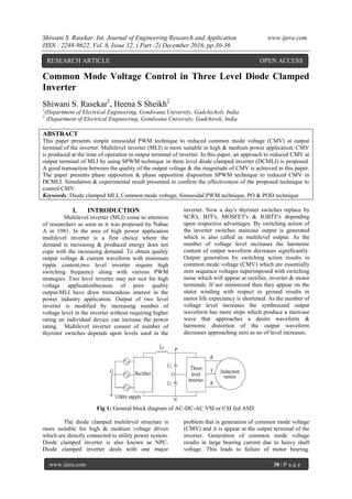
  • 1. Shiwani S. Rasekar. Int. Journal of Engineering Research and Application www.ijera.com ISSN : 2248-9622, Vol. 6, Issue 12, ( Part -2) December 2016, pp.30-36 www.ijera.com 30 | P a g e Common Mode Voltage Control in Three Level Diode Clamped Inverter Shiwani S. Rasekar1 , Heena S Sheikh2 1 (Department of Electrical Engineering, Gondwana University, Gadchicholi, India 2 (Department of Electrical Engineering, Gondwana University, Gadchiroli, India ABSTRACT This paper presents simple sinusoidal PWM technique to reduced common mode voltage (CMV) at output terminal of the inverter. Multilevel inverter (MLI) is more suitable in high & medium power application, CMV is produced at the time of operation in output terminal of inverter. In this paper, an approach to reduced CMV at output terminal of MLI by using SPWM technique in three level diode clamped inverter (DCMLI) is proposed. A good transaction between the quality of the output voltage & the magnitude of CMV is achieved in this paper. The paper presents phase opposition & phase opposition disposition SPWM technique to reduced CMV in DCMLI. Simulation & experimental result presented to confirm the effectiveness of the proposed technique to control CMV. Keywords: Diode clamped MLI, Common mode voltage, Sinusoidal PWM technique, PO & POD technique. I. INTRODUCTION Multilevel inverter (MLI) come to attention of researchers as soon as it was proposed by Nabae A in 1981. In the area of high power application multilevel inverter is a first choice where the demand is increasing & produced energy does not cope with the increasing demand. To obtain quality output voltage & current waveform with minimum ripple content,two level inverter require high switching frequency along with various PWM strategies. Two level inverter may not suit for high voltage applicationbecause of poor quality output.MLI have draw tremendous interest in the power industry application. Output of two level inverter is modified by increasing number of voltage level in the inverter without requiring higher rating an individual device can increase the power rating. Multilevel inverter consist of number of thyrister switches depends upon levels used in the inverter. Now a day's thyrister switches replace by SCR's, BJT's, MOSFET's & IGBTE's depending upon respective advantages. By switching action of the inverter switches staircase output is generated which is also called as multilevel output. As the number of voltage level increases the harmonic content of output waveform decreases significantly. Output generation by switching action results in common mode voltage (CMV) which are essentially zero sequence voltages superimposed with switching noise which will appear at rectifier, inverter & motor terminals. If not minimized then they appear on the stator winding with respect to ground results in motor life expectancy is shortened. As the number of voltage level increases the synthesized output waveform has more steps which produce a staircase wave that approaches a desire waveform & harmonic distortion of the output waveform decreases approaching zero as no of level increases. Fig 1: General block diagram of AC-DC-AC VSI or CSI fed ASD. The diode clamped multilevel structure is more suitable for high & medium voltage drives which are directly connected to utility power system. Diode clamped inverter is also known as NPC. Diode clamped inverter deals with one major problem that is generation of common mode voltage (CMV) and it is appear at the output terminal of the inverter. Generation of common mode voltage results in large bearing current due to heavy shaft voltage. This leads to failure of motor bearing. RESEARCH ARTICLE OPEN ACCESS
  • 2. Shiwani S. Rasekar. Int. Journal of Engineering Research and Application www.ijera.com ISSN : 2248-9622, Vol. 6, Issue 12, ( Part -2) December 2016, pp.30-36 www.ijera.com 31 | P a g e Therefore best solution for this problem is only to eliminate CMV permanently.Variable frequency ,variable voltage require in industrial application , medium and high voltage level supply given to three phase induction motors.multilevel inverter have been establish better counterpart to conventional two level inverters. Recently number of techniques are used to eliminate common mode voltage, but in all the techniques SPWM techniques is more suitable.In this paper common mode voltage reduction techniques for three level diode clamped inverter is represented by using SPWM technique. II. BACKGROUND 2.1.Three Level Diode Clamped Inverter: In high voltage & high power application diode clamped multi level inverter(DCMLI) become a research hotspot. Multi level inverter is preferred in between three to nine level inverter. As the number of voltage level increases total harmonic distortion is reduced.Three level inverter is shown in diagram below. Fig 2: Schematic diagram of three phase, three level diode-clamped inverter. Three phase diode clamped MLI have three legs with common DC bus, this DC voltage is subdivided into switching capacitors. Each diode has to block the voltage equal to number of switching above it times the supplied DC voltage. Basically one leg of DCMLI consist of 'M-1' capacitors & 'M-2' clamping diodes where 'M' is the total voltage levels & total number of switches are 2(M-1), in the three level inverter number of switches used are 12, for the operation in numbering order of Sa1, Sa2, Sb1, Sb2, Sc1, Sc2, Sa1', Sa2', Sb1', Sb2', Sc1' & Sc2'. Dc bus consist of two capacitors C1 & C2, six diodes are used two for each leg. In DCMLI diode is used as clamping device to clamp the dc bus voltage so as to achieve staircase output voltage as shown in the diagram. Fig 3: Staircase output of the Three level inverter.
  • 3. Shiwani S. Rasekar. Int. Journal of Engineering Research and Application www.ijera.com ISSN : 2248-9622, Vol. 6, Issue 12, ( Part -2) December 2016, pp.30-36 www.ijera.com 32 | P a g e 2.2.Common Mode Voltage: Common mode voltage is defined as the voltage between neutral point of the load & system ground. It may also defined as the voltage between neutral point of the load & dc midpoint given diagram shows generalized drive system , where Vag, Vbg & Vcg are the voltages between ground to phase & Vng is the voltage between neutral point of the motor and system ground. i. e. CMV & it is given as: CMV = Vng = (Two level inverter) CMV = Vng = (Three level inverter) CMV= Vng = (Five level inverter). Output of the inverter is not purely sinusoidal but square wave (discrete) , hence sum of the instantaneous value is not zero & develops common mode voltage. Meanwhile in purely sinusoidal three phase system sum of the instantaneous voltage is zero hence CMV is zero. Neutral point voltage variation results in generation of common mode voltage three times the fundamental frequency. If common mode voltages are not reduces they results in bearing failure of the motor connected as load in output terminal. Fig 4: Three phase VSI inverter with Induction motor connected as a load. III. CMV CONTROL STRATEGIES Control strategies for common mode voltage can be classified as given below: 1. Using some extra hardware circuitry such as isolation transformer, active passive filter, common mode choke &dual bridge inverter etc. 2. Using modification in control strategy such as space vector PWM technique (SVPWM) & sinusoidal PWM technique (SPWM). In the first method common mode voltage is minimized by selecting proper rating of the chock, but the main issue is that the total harmonic distortion (THD) increases with controlling CMV. Fig 5: Sinusoidal pulse width modulation technique
  • 4. Shiwani S. Rasekar. Int. Journal of Engineering Research and Application www.ijera.com ISSN : 2248-9622, Vol. 6, Issue 12, ( Part -2) December 2016, pp.30-36 www.ijera.com 33 | P a g e High frequency triangular carrier signals superimposed with three sinusoidal reference signal known as the modulating signals to generates the gating signal for the inverter switches this process known as sinusoidal PWM technique. SPWM technique provides effective switching frequency of load voltage is 3 times the switching frequency of each cell as determine by its carrier signal & require less complex algorithm with ease to implement. Instead of maintaining width of all pulses same as in case of multiple pulse width modulation, the width of each pulse is varied in proportion to the amplitude of sine wave evaluate at the center at the same pulse. The distortion & lower order harmonics are reduced significantly. The gating signal generated by comparing sinusoidal reference signal with triangular carrier wave. When instantaneous value of the sine reference is greater than the triangular carrier wave then the output is at +Vdc & when the reference signal is less than the carrier signal then the output is at -Vdc. Different SPWM technique can be classified as: a. Phase disposition method b. Phase shifted method c. Phase opposition disposition method. 3.1 Phase disposition method: Phase disposition method based on the comparison of sinusoidal reference waveform with triangular carrier waveform, all the carrier waveform have same frequency and amplitude & all the carrier waves are in phase with each other. If 'M' is the number of voltage level in inverter then 'M-1' carrier signals are used to generate voltage levels. Fig 6: Phase disposition PWM technique. 3.2 Phase opposition disposition: In this method sinusoidal reference wave superimposed on the carrier triangular wave (which are phase above & below the zero reference) like in phase opposition method but difference is that, triangular wave above & below the reference zero axis have equal frequency and amplitude but they are phase shifted by 180 degree with each other. The reference signal is compared with all carrier waves thus gate pulses are generated & are related into each switching device. Fig 7: Phase opposition disposition SPWM technique
  • 5. Shiwani S. Rasekar. Int. Journal of Engineering Research and Application www.ijera.com ISSN : 2248-9622, Vol. 6, Issue 12, ( Part -2) December 2016, pp.30-36 www.ijera.com 34 | P a g e IV. EXPERIMENTAL RESULTS Figure shows the simulation diagram of the proposed inverter. The circuit is designed in Matlab/simulink and the generation of pulses has been made by comparing every carrier wave with the sine wave and the resultant pulses has been given to the appropriate switches to produce the three level staircase waveform . Fig 8: Simulation diagram for proposed 3 level MLI Diagram below shows experimental results of three level diode clamped inverter common mode voltage reduction by PD-SPWM technique with & without filter. Fig 9 shows output of inverter which is staircase wave. Sinusoidal waveform obtain after filtering inverter output. Fig 9: Output waveform of proposed MLI using PD technique. Fig 10: Filtered output waveform of proposed MLI
  • 6. Shiwani S. Rasekar. Int. Journal of Engineering Research and Application www.ijera.com ISSN : 2248-9622, Vol. 6, Issue 12, ( Part -2) December 2016, pp.30-36 www.ijera.com 35 | P a g e Fig11: FFT analysis of proposed technology using PD technique. The total harmonic distortion (THD) of any waveform is define as the closeness to the fundamental wave shape. FFT analysis is done to determine the THD of the output waveform. Fig 12: Output waveform of proposed MLI using POD technique. Fig 13:Filtered output waveform of MLI. Fig 14: FFT analysis of proposed technology using POD technique.
  • 7. Shiwani S. Rasekar. Int. Journal of Engineering Research and Application www.ijera.com ISSN : 2248-9622, Vol. 6, Issue 12, ( Part -2) December 2016, pp.30-36 www.ijera.com 36 | P a g e Phase opposition disposition method uses reference wave & carrier wave, carrier waves are 180 degree phase opposite to each other. Comparing reference signal with carrier wave results in gating pulses shown in diagram. Fig. 13 shows filtered output of the MLI. Table 1: Comparison between PD & POD technique. SPWM Technique THD CMV Without Filter With Filter PD 45.13 0.77 Vdc/2 POD 85.36 18.58 Vdc/2 V. CONCLUSION The proposed technique reduces CMV at the output terminal of the DCMLI. Experimental results & simulation shows the effectiveness of the proposed techniques giving reduction in magnitude of common mode voltage. Results prove that PO- SPWM technique is superior to reduced Total harmonic distortion & CMV. REFERENCES [1] Xiaoming Yuan, member, IEEE & Ivo babri, senior member IEEE, "Fundamental of new diode clamping multilevel inverter," IEEE transaction on power electronics, vol 15, no. 4, july 2000. [2] F. Wang, "Sine triangle versus space vector modulation for three-level PWM voltage source inverters," IEEE Transactions on Industry Application, vol. 38, no.2, pp.500- 506,2002. [3] P.C.Loh, D.G.Holmes Y. Fukuta, and T. A. Lipo, "Reduced common mode modulation strategies for cascaded multilevel inverter," IEEE Transaction on industrial application, vol.39, no.5, pp. 1386-1395, 2003. [4] Chenggang Mei, Juan Carlos Balda, and William P. Waite, "Cancellation of common mode voltages for induction motor drives using active method ," IEEE Trans. Energy Conversion, Vol.21, pp. 380-386, Jun. 2006. [5] R. S. Kanchan, P. N. Teckwani and K. Gopakumar," Three level inverter scheme with common mode voltage elimination and dc link capacitor voltage balancing for an open-end winding induction motor drive," IEEE Transaction on power electronics, vol.21, no. 6, pp. 1676- 1683,2006. [6] A. Videt, P. Le Moigen, N. Idir P. Baudesson, and X. Cimetire, "A new carrier-based PWM providing common mode-current reduction and DC-bus balancing for three-level inverter," IEEE Transaction on Industrial Electronics, vol. 54, no. 6, pp.3001-3011,2007. [7] Jose Roriguez Steffen Bernet, Bin Wu, Joege O. Pontt and Samir Kouro, " Multilevel voltage -source-converter topologies for industrial medium voltage drive", IEEE Trans. Indl. Electron, Vol. 54, No. 6, pp. 2930-2944, Dec. 2007. [8] Pradyumn Chaturvedi, Shailendra & pramod Agrawal,"Carrier based CMV control techniques in three level diode clampd inverter," Advances in power electronics, 2012, pages 12. [9] Z. Zhao, Y. Zhong, H. Gao, L. Yuan and T. Lu, "Hybrid selective harmonic elimination PWM for common mode voltage in three level neutral point clamped inverter for variable speed induction drives," IEEE Transaction on power electronics, vol. 27, no. 3, pp. 1152-1158,2012. [10] Jayant M Parkhi, R.K.Dhatrak, "Reduction of common mode voltage in AC drive using MLI," IJERA, vol. 3, isuue 4, Jul- Aug 2013, pp. 212-218. [11] Akash A. Chndekar, R.K.Dhatrak, Z.J.Khan, "Modelling & simulation of diode clamped multiinverter fed three phase induction motor for CMV analysis using filter," IJAREEIE, vol.2, issue8, Aug 2013. [12] C. Bharatiraja, K.V.R.S.. Prakara Rao, Dr. S. Jeevanthan, "Reduction of common mode voltage in three level neutral point diode clamped multilevel inverter using space vector pulse width modulation, " IJCEEE, vol 1, issue 2, Dec 2013. [13] M. S. Raghuvendra Reddy, G. Sri. Harsha, B. Nishanth, E. Sai. Pratik Reddy, "Common mode voltage reduction in DCMLI," IJETT, vol 11, No. 2, May 2014. [14] Darshan Prajapati, Vineetha Ravindra, Jil sutaria, Pratik patel, "A comparitive study of three phase 2 level VSI with 3 level & 5 level diode clamped multilevel inverter," IJETAE, vol 4, issue 4, april 2014. [15] S. Devraj, Dr Anitha G. S. , "POD-PWM based capacitor clamped multilevel inverter," IJTRA, vol 3, issue 4, 2015, pp. 80-82.