![Article Crystal Growth & Design, Vol. 10, No. 10, 2010 4443
(FTO)-covered glass. The size of the coated substrates was about
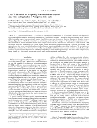
3 cm  1.1 cm). Substrates were cleaned by immersion in detergent
solution (Alcanox detergent powder) at 90 °C for 20 min and then
sonicated at room temperature in the same solution for an addi-
tional 20 min. The substrates were then rinsed followed by sonica-
tion for 20 min in 18 MΩ Millipore purified water (DDW). Instead
of the treatment described above, some samples were sonicated for
10 min each in acetone, ethanol, and DDW with no apparent
difference in film uniformity or morphology. The cleaned substrates
were next activated by immersion in 15 mL of a 0.5 mM aqueous
KMnO4 solution containing 60 μL of n-butanol (0.044 M
n-butanol) at 90 °C for 25 min. Afterward, substrates were rinsed,
sonicated for 5 min, and rinsed again (all in DDW) to remove any Figure 1. ZnO film on FTO deposited for 60 min: cross section (A)
permanganate residues. This process forms Mn oxide particles on and top view (B).
the substrate that act as nucleation centers for the ZnO growth.9 As
will be described below, this activation is not necessary because Sb
species in the solution are themselves effective nucleation initiators.
However, we continued to use it as the activation was part of many
earlier experiments, and more importantly, Sb-free films, with
which we compared these Sb-containing films, could be deposited
on only a preactivated substrate.
Film Deposition. ZnO films were deposited on the basis of a
modification of the method presented in ref 9. Zn(NO3)2 [1 M,
98.5% (Merck)], 0.01 M KSbOC4H4O6 [antimony potassium (þ)
tartrate, 99.5% (BDH)], 1 M ethylenediamine [EDA, 99.5%
(Fluka)], and 8.24 M (50% by volume) ethanolamine [EA, 99.5%
(Merck)] were used as precursors for deposition. Unless stated
otherwise, 10-15 mL solutions with the following compositions
were used: 0.1 M Zn, 1.65 M EA, and 0.15 M EDA for ZnO
films and 0.1 M Zn, 0.001 M Sb (i.e., 1 at. % Sb with respect to Zn
concentration), 1.65 M EA, and 0.12 M EDA for ZnO:Sb films.
Some depositions were conducted using NH4OH (Merck 25%) in
place of EDA. For these baths, the deposition solutions contained
0.6 and 0.4 M NH4OH for ZnO and ZnO:Sb films, respectively. The
pH of all baths used here was in the range of 11.2-11.4 (this is the
natural pH of the baths and is determined mainly by the complex-
Figure 2. ZnO film evolution. Films deposited for 5, 10, 20, 30, 40,
ants used).
and 60 min (A-F, respectively).
Activated substrates were placed tilted and face down in plastic
vials to prevent precipitate in the bath from depositing on the Results and Discussion
desired (downward-facing) side. The plastic vials were tightly closed
to prevent evaporation of the deposition solution and loss of volatile ZnO Films. As previously shown using the alkaline,
reactants. Deposition was conducted at 90 °C for various times, ethanolamine-based bath, the CBD ZnO morphology is
most commonly 90 min for full film thickness, in a temperature-
controlled water bath. Finally, samples were rinsed in DDW and
strongly dependent, among other parameters, on the zinc salt
dried in a N2 flow. anion, substrate surface “activation”, and even the material of
Film Characterization. The films were initially inspected visually the reaction vessel.15 For the specific parameters used in this
for macroscale coverage. High-resolution scanning electron micro- study, ZnO films grow as pointed tip nanorods and have a
scopy (SEM) imaging using a Ziess Ultra 55 apparatus was per- terminal thickness of ca. 4 μm after deposition for 60 min
formed for morphology inspection. A Rigaku RU300 rotating (Figure 1). No homogeneous precipitation was noticed in
anode X-ray diffractometer was used for X-ray diffraction (XRD) parallel with deposition.
in a 2θ-θ specular scan mode. Transmission electron microscopy
(TEM) cross-section sample preparation was conducted using a
As is common for this deposition, initial growth is random
FEI Helios dual-beam focused ion beam (FIB). TEM imaging and and denser, with increasing directionality of the nanorods as
selected area electron diffraction were conducted on a Philips the film evolves. This increasing directionality is presumed to
CM120 transmission electron microscope using a 120 kV electron be due to termination of growth of nonperpendicular rods
beam. The selected area was ca. 90 nm in diameter for EDS and ca. when their growth is blocked by other rods. Most perpen-
60 nm in diameter for electron diffraction. High-resolution TEM dicular rods, in contrast, continue to grow undisturbed.
(HRTEM) imaging was performed on a FEI Tecnai F30 U-Twin Figure 2 shows how the film morphology develops with time
microscope with a 300 kV electron beam. Elemental analysis was and will be considered later when comparing films deposited
conducted using an energy dispersive spectroscopy (EDS) EDAX-
Phoenix detector mounted on the CM120 transmission electron from Sb-free and Sb-containing solutions. The evolution of
microscope and by X-ray photoelectron spectroscopy (XPS) ana- the film is accompanied by little change in nanorod shape
lysis using a Kratos ULTRA with monochromatic Al KR (1486.6 (more detail about the individual nanorod morphology is
eV) radiation. The composition of the solution was examined with a presented in Figure SI 1 of the Supporting Information).
PerkinElmer ELAN9000 inductively coupled plasma/mass spectro- Deposition of ZnO from an ammonia bath was character-
meter. The sample for inductively coupled plasma/mass spectro- ized by a similar evolution, although the nanorods are longer
metry (ICP-MS) was prepared via addition of 50 μL of the and thicker than for the EDA bath, and the shape of the tips
deposition solution to 0.3 mL of 69% HNO3 and addition of
of the rods is different for the two baths (Figure 3). The
10 mL of DDW after ∼16 h. Two solutions were used as blanks:
(a) 0.3 mL of HNO3 and 10 mL of DDW and (b) 50 μL of the increased length of the nanorods is presumably related to
deposition solution to which no Sb was added with 0.3 mL of HNO3 the stronger complex Zn2þ forms with EDA compared with
and 10 mL of DDW. Standard solutions of Zn and Sb ions were used the complex with ammonia, leading to an overall lower
to calibrate the inductively coupled plasma/mass spectrometer. growth rate.](data:image/gif;base64,R0lGODlhAQABAIAAAAAAAP///yH5BAEAAAAALAAAAAABAAEAAAIBRAA7)
Recommended
Recommended
More Related Content
What's hot
What's hot (12)
Viewers also liked
Viewers also liked (17)
Similar to Kedem Et Al. 2010 Effect of Sb Ions on the Morphology of Chemical Bath-Deposited ZnO Films and Application to Nanoporous Solar Cells
Similar to Kedem Et Al. 2010 Effect of Sb Ions on the Morphology of Chemical Bath-Deposited ZnO Films and Application to Nanoporous Solar Cells (20)
Kedem Et Al. 2010 Effect of Sb Ions on the Morphology of Chemical Bath-Deposited ZnO Films and Application to Nanoporous Solar Cells
- 1. DOI: 10.1021/cg100636j Effect of Sb Ions on the Morphology of Chemical Bath-Deposited 2010, Vol. 10 ZnO Films and Application to Nanoporous Solar Cells 4442–4448 Nir Kedem,† Eran Edri,† Michael Kokotov,† Hagai Cohen,‡ Tatyana Bendikov,‡ Ronit Popovitz-Biro,‡ Palle von Huth,‡ David Ginley,§ and Gary Hodes*,† † Department of Materials and Interfaces, Weizmann Institute of Science, Rehovot 76100, Israel, ‡ Department of Chemical Research Support, Weizmann Institute of Science, Rehovot 76100, Israel, and § National Renewable Energy Laboratory, 1617 Cole Boulevard, Golden, Colorado 80401-3393 Received May 11, 2010; Revised Manuscript Received August 26, 2010 ABSTRACT: Low concentrations (0.1-1% of the Zn concentration) of Sb ions in an alkaline ZnO chemical bath deposition solution were found to lead to pronounced changes in the ZnO film morphology. The tapered nanorods obtained in the absence of Sb become flat-topped and more closely packed when Sb is present, and the nanorod diameter changes, the direction of these changes depending on other bath parameters. An initial compact layer that was comprised of very small nanocrystals is formed. Sb was found to be present in the films, mostly in the compact initial layer. We postulate that initial Sb-rich nuclei promote ZnO nucleation but retard subsequent ZnO crystal growth. As the Sb concentration (relative to the Zn) in the bath drops, ZnO nanorods can then grow, but with altered morphology because of preferential adsorption of the low levels of Sb in solution on (002) ZnO crystal faces. These films were found to be very suitable for solid state semiconductor-sensitized solar cells. Such cells normally require a separate deposition of a blocking compact layer before the nanoporous layer. The initial in situ compact layer in our films is very efficient for this purpose, giving much more reproducible performance. Introduction sticking coefficient for other constituents in the solution. There are a number of studies in which foreign atoms or While commonly grown and utilized as an n-type semicon- molecules in the deposition solution were found to influence ductor, the potential p-type ZnO has drawn much attention in the morphology of CBD ZnO films. The presence of citrate is the past few years for its application to technologies such as known to lead to flat crystals instead of the textured rod UV-LEDs and lasers, transparent electronics, and optoelec- morphology most commonly observed.6,7 Different anions tronics. The primary purpose of doping ZnO in general is result in very appreciable differences in nanorod diameter,8,9 to modify its electrical and optoelectronic properties. While probably due, at least in part, to differences in specific less commonly considered, in situ doping can also affect adsorption of the different anions on the growing crystals. ZnO growth and morphology. The ability to control the film There are a couple of studies describing the effect of cations on morphology is crucial for photovoltaic (PV) devices such as CBD ZnO films. In one, Cd ions change the film morphology extremely thin absorber (ETA), organic photovoltaic (OPV), and from thin rods to thicker and flatter crystals.10 In another, the dye-sensitized solar cells. In all of these devices, the large surface addition of Mg leads to differences in film texture and small area of the absorber greatly improves device performance. morphology changes.11 In both cases, little or none of the Chemical bath deposition (CBD), where the term CBD is foreign cation was present in the final ZnO film. We also note taken to globally include liquid phase deposition and hydro- a study on the effects of different cations on hydrothermally thermal deposition of films, is a common method used to deposit grown (230-300 °C) ZnO precipitates,12 an approach that has nanostructured ZnO films. While there are many different some similarities to CBD growth. In that study, the different “recipes” for this deposition, they are almost all performed in cations resulted in a number of different crystal shapes, aqueous solutions at relatively high temperatures (typically although in general they were based on pyramidal growth. 70-90 °C) and in general are believed to be based on formation In this work, deposition of the ZnO films was based on the of hydroxylated Zn species that at the reaction temperature controlled release of Zn ions into a highly alkaline solution. At readily forms ZnO directly. high pH, Zn readily forms a hydroxide that at elevated In spite of the large number of papers published on CBD temperatures forms ZnO. Complexants were used to prevent ZnO, only a very small number deal with the incorporation of immediate precipitation of Zn(OH)2 in the solution and also substitutional dopants into ZnO1-5 (ref 5 describes a two-step to adjust pH to obtain uniform deposition conditions. process in which doping occurs after ZnO deposition). The This research was initiated with the intention of attempting dopant species can also affect the morphology of the growing to dope CBD ZnO p-type using Sb. Sb has been found to dope ZnO film. This is usually considered to occur by preferential ZnO p-type13,14 in general, and there is one study suggesting adsorption of the dopant species in the deposition solution on p-type ZnO:Sb films by CBD.3 We have found that the Sb specific planes of the growing ZnO (or ZnO precursor) crystal, “impurities” had major effects on the growth mode of the ZnO although it could also affect the crystal surface energy and/or films, and this paper describes these effects. *To whom correspondence should be addressed: Department of Experimental Section Materials and Interfaces, Weizmann Institute of Science, Rehovot 76100, Israel. Telephone: þ972-8-9342076. Fax: þ972-8-9344137. E-mail: gary. Substrate Cleaning and Activation. Films were deposited either on hodes@weizmann.ac.il. soda-lime glass microscope slides or on fluorine-doped tin oxide pubs.acs.org/crystal Published on Web 09/21/2010 r 2010 American Chemical Society
- 2. Article Crystal Growth & Design, Vol. 10, No. 10, 2010 4443 (FTO)-covered glass. The size of the coated substrates was about 3 cm  1.1 cm). Substrates were cleaned by immersion in detergent solution (Alcanox detergent powder) at 90 °C for 20 min and then sonicated at room temperature in the same solution for an addi- tional 20 min. The substrates were then rinsed followed by sonica- tion for 20 min in 18 MΩ Millipore purified water (DDW). Instead of the treatment described above, some samples were sonicated for 10 min each in acetone, ethanol, and DDW with no apparent difference in film uniformity or morphology. The cleaned substrates were next activated by immersion in 15 mL of a 0.5 mM aqueous KMnO4 solution containing 60 μL of n-butanol (0.044 M n-butanol) at 90 °C for 25 min. Afterward, substrates were rinsed, sonicated for 5 min, and rinsed again (all in DDW) to remove any Figure 1. ZnO film on FTO deposited for 60 min: cross section (A) permanganate residues. This process forms Mn oxide particles on and top view (B). the substrate that act as nucleation centers for the ZnO growth.9 As will be described below, this activation is not necessary because Sb species in the solution are themselves effective nucleation initiators. However, we continued to use it as the activation was part of many earlier experiments, and more importantly, Sb-free films, with which we compared these Sb-containing films, could be deposited on only a preactivated substrate. Film Deposition. ZnO films were deposited on the basis of a modification of the method presented in ref 9. Zn(NO3)2 [1 M, 98.5% (Merck)], 0.01 M KSbOC4H4O6 [antimony potassium (þ) tartrate, 99.5% (BDH)], 1 M ethylenediamine [EDA, 99.5% (Fluka)], and 8.24 M (50% by volume) ethanolamine [EA, 99.5% (Merck)] were used as precursors for deposition. Unless stated otherwise, 10-15 mL solutions with the following compositions were used: 0.1 M Zn, 1.65 M EA, and 0.15 M EDA for ZnO films and 0.1 M Zn, 0.001 M Sb (i.e., 1 at. % Sb with respect to Zn concentration), 1.65 M EA, and 0.12 M EDA for ZnO:Sb films. Some depositions were conducted using NH4OH (Merck 25%) in place of EDA. For these baths, the deposition solutions contained 0.6 and 0.4 M NH4OH for ZnO and ZnO:Sb films, respectively. The pH of all baths used here was in the range of 11.2-11.4 (this is the natural pH of the baths and is determined mainly by the complex- Figure 2. ZnO film evolution. Films deposited for 5, 10, 20, 30, 40, ants used). and 60 min (A-F, respectively). Activated substrates were placed tilted and face down in plastic vials to prevent precipitate in the bath from depositing on the Results and Discussion desired (downward-facing) side. The plastic vials were tightly closed to prevent evaporation of the deposition solution and loss of volatile ZnO Films. As previously shown using the alkaline, reactants. Deposition was conducted at 90 °C for various times, ethanolamine-based bath, the CBD ZnO morphology is most commonly 90 min for full film thickness, in a temperature- controlled water bath. Finally, samples were rinsed in DDW and strongly dependent, among other parameters, on the zinc salt dried in a N2 flow. anion, substrate surface “activation”, and even the material of Film Characterization. The films were initially inspected visually the reaction vessel.15 For the specific parameters used in this for macroscale coverage. High-resolution scanning electron micro- study, ZnO films grow as pointed tip nanorods and have a scopy (SEM) imaging using a Ziess Ultra 55 apparatus was per- terminal thickness of ca. 4 μm after deposition for 60 min formed for morphology inspection. A Rigaku RU300 rotating (Figure 1). No homogeneous precipitation was noticed in anode X-ray diffractometer was used for X-ray diffraction (XRD) parallel with deposition. in a 2θ-θ specular scan mode. Transmission electron microscopy (TEM) cross-section sample preparation was conducted using a As is common for this deposition, initial growth is random FEI Helios dual-beam focused ion beam (FIB). TEM imaging and and denser, with increasing directionality of the nanorods as selected area electron diffraction were conducted on a Philips the film evolves. This increasing directionality is presumed to CM120 transmission electron microscope using a 120 kV electron be due to termination of growth of nonperpendicular rods beam. The selected area was ca. 90 nm in diameter for EDS and ca. when their growth is blocked by other rods. Most perpen- 60 nm in diameter for electron diffraction. High-resolution TEM dicular rods, in contrast, continue to grow undisturbed. (HRTEM) imaging was performed on a FEI Tecnai F30 U-Twin Figure 2 shows how the film morphology develops with time microscope with a 300 kV electron beam. Elemental analysis was and will be considered later when comparing films deposited conducted using an energy dispersive spectroscopy (EDS) EDAX- Phoenix detector mounted on the CM120 transmission electron from Sb-free and Sb-containing solutions. The evolution of microscope and by X-ray photoelectron spectroscopy (XPS) ana- the film is accompanied by little change in nanorod shape lysis using a Kratos ULTRA with monochromatic Al KR (1486.6 (more detail about the individual nanorod morphology is eV) radiation. The composition of the solution was examined with a presented in Figure SI 1 of the Supporting Information). PerkinElmer ELAN9000 inductively coupled plasma/mass spectro- Deposition of ZnO from an ammonia bath was character- meter. The sample for inductively coupled plasma/mass spectro- ized by a similar evolution, although the nanorods are longer metry (ICP-MS) was prepared via addition of 50 μL of the and thicker than for the EDA bath, and the shape of the tips deposition solution to 0.3 mL of 69% HNO3 and addition of of the rods is different for the two baths (Figure 3). The 10 mL of DDW after ∼16 h. Two solutions were used as blanks: (a) 0.3 mL of HNO3 and 10 mL of DDW and (b) 50 μL of the increased length of the nanorods is presumably related to deposition solution to which no Sb was added with 0.3 mL of HNO3 the stronger complex Zn2þ forms with EDA compared with and 10 mL of DDW. Standard solutions of Zn and Sb ions were used the complex with ammonia, leading to an overall lower to calibrate the inductively coupled plasma/mass spectrometer. growth rate.
- 3. 4444 Crystal Growth & Design, Vol. 10, No. 10, 2010 Kedem et al. Figure 3. ZnO film deposited for 90 min from an EDA (top) or Figure 5. ZnO:Sb films deposited for 90 min from EDA (A-C) ammonia (bottom) bath. and ammonia (D-F) baths. (A and D) Cross section of the films. (B and E) Plan view and (C and F) higher magnification of the nanorod tips. Figure 4. ZnO:Sb film deposited from an EDA bath for 15 h on glass (detached from the substrate). Bath composition: 0.1 M Zn, 0.001 M Sb, 1.65 M EA, and 0.15 M EDA. Figure 6. ZnO:Sb films deposited for 5, 10, 20, and 30 min (cross section and plan view) and 40, 50, 70, and 90 min (cross section ZnO:Sb Films. Because Sb was added as antimony potas- only). sium tartrate, the effect of tartrate (0.001 M potassium sodium tartrate, BDH 99%) on the morphology of ZnO By lowering the concentration of the complexants (i.e., films was first examined. For films grown from an EDA changing from the ZnO bath to the ZnO:Sb bath as described bath, only a small effect, seen as a slight broadening of the in the Experimental Section), a few micrometer thick ZnO: nanorods, was observed. A much more significant effect was Sb film could be obtained after 90 min. The ZnO columnar found for films grown from an ammonia bath. In that case, crystals obtained from the Sb-containing bath were not the nanorod diameter increased significantly and their ends pointed, but rather straight-sided and flat-topped (more so became stepped and nearly flat rather than pointed (Figure SI for the EDA than for the ammonia bath), and more densely 2 of the Supporting Information). Unless specifically stated packed, as shown in Figure 5. A slight homogeneous pre- otherwise, the results below refer to films grown from an cipitation was observed in the deposition solution for both EDA bath. More detailed information regarding the effect of complexants. More importantly, deposition also occurred tartrate on CBD ZnO will be published separately. on the walls of the reaction vials. The difference between Adding 1 at. % Sb (wurtzite Zn concentration) to the basic the two complexes, manifested by the thicker and longer ZnO bath resulted in only a very thin (few nanometers) columns obtained using the ammonia complex in the Sb-free yellowish and transparent film (Figure SI 3 of the Supporting films, was much smaller when Sb was added. Information). Longer deposition times of 12-15 h resulted We note that Sb concentrations ranging from 0.1 to 3% in films with a maximum thickness of 1 μm and with a were examined. Film evolution and morphology were qua- morphology very different from that of the Sb-free ZnO films litatively similar for Sb contents ranging from 0.5 to 3%. The (which reach maximum thickness after ca. 1.5 h) (Figure 4). results shown in this paper are for 1% Sb (with respect to Zn). The rods were thicker, shorter, and more tortuous than the The evolution of film growth was also different for the straight crystals typical of the Sb-free bath. They were also ZnO:Sb and Sb-free films, with two distinct growth modes somewhat rough and porous with many small holes in the for the ZnO:Sb films rather than the single mode seen in the crystals. These crystals grew on an initially formed relatively ZnO. In the first 30-40 min of deposition, a ca. 200 nm thick (>0.5 μm) very compact film. The adhesion of these compact, continuous layer develops, followed by rapid films on glass was poor, and they often spontaneously peeled growth of columnar crystals to a thickness of a few micro- off the substrate, in contrast to the good adhesion obtained meters (Figure 6). The thickness of the compact layer varies for the same films on FTO. with the concentration of Sb in the deposition solution.
- 4. Article Crystal Growth & Design, Vol. 10, No. 10, 2010 4445 Figure 9. (A) SEM cross section showing the regions from which the electron diffraction patterns were acquired. (B and C) ED patterns from region b (bottom compact layer) and region c (top) as labeled in panel A. Figure 7. XRD pattern of ZnO:Sb (black) and ZnO (gray) films deposited on glass, where the highest (002) peaks are normalized. Figure 10. Cross-sectional TEM images of the initial (compact layer) growth of a ZnO:Sb film at two different magnifications. an ammonia bath, although the morphologies slightly differ between the two. To understand the nature of this nucleation step for the ZnO:Sb films, we conducted various compositional and phase analyses on different parts of the samples. We already noted above that XRD of the initial compact layer formed in the Sb-containing film showed no peaks. Electron diffraction (ED) is in general more sensitive for small amounts of sampled material. We compared ED of a cross-sectional sample where Figure 8. Double ZnO layers (top/bottom): (A) ZnO/ZnO, (B) the initial compact layer and the clearly crystalline top layer ZnO:Sb/ZnO, (C) ZnO/ZnO:Sb, and (D) ZnO:Sb/ZnO:Sb films. were sampled separately (panels B and C of Figure 9, re- XRD analyses of the initial thin compact film showed no spectively). Both analyses showed the wurtzite ZnO diffraction signal, even using slow scan rates and multiple scans or pattern. The ED of the upper crystalline layer showed a pattern grazing angle incidence as would be commonly done for like that of a single crystal, which would be expected from small nanocrystals. Fully grown films revealed no indication a selected area (60 nm) smaller than the size of a single of any phases other than wurtzite ZnO for Sb-containing as ZnO crystal. The compact layer showed a more diffuse, more well as Sb-free films. Highly textured growth in the direction polycrystalline pattern, with some degree of orientation (seen of the c-axis [perpendicular to the (002) crystal face] was by concentration of intensity into arcs), and only ZnO was found in both cases, with the degree of texture considerably observed (no Sb oxide). The broad and diffuse pattern of the higher in the ZnO:Sb films (Figure 7). This increase in the compact layer suggests very small crystals. TEM cross- level of texture of the films can be explained by the closer sectional images of the compact layer show grains ∼5 nm in packing of crystals, thus allowing less growth of nonperpen- size (Figure 10A) and, under higher magnification, single- dicular crystals. crystal ZnO regions typically 5 nm in size (Figure 10B). The role of Sb in retarding and modifying ZnO deposition, ICP-MS analysis of the deposition solution composition by affecting nucleation or growth, was examined by deposi- as a function of film growth (Figure 11) confirms much of the tion of doubly layered films. Four films were deposited: Sb (roughly half) is deposited in the thin, initial compact ZnO/ZnO, ZnO:Sb/ZnO:Sb, ZnO/ZnO:Sb, and ZnO:Sb/ layer. At the end of the deposition, the Sb content in the ZnO. The first term in each pair represents the second solution decreases to 7% of its initial value, while the final Zn (top) layer. Deposition of a ZnO layer over either ZnO concentration is 50-60% of the initial value. (Figure 8A) or ZnO:Sb (8c) films resulted in further growth TEM/EDS was performed at several points on the cross of the existing crystals. In contrast, deposition of a ZnO:Sb section as described in Table 1. The Sb concentration layer over either ZnO (Figure 8B) or ZnO:Sb films decreased gradually from ca. 6-9% (wurtzite Zn con- (Figure 8D) resulted in the formation of a clear interface centration) in the compact layer to ca. 1% at the top of the between the two. At the interface, a new nucleation step was film. The ca. 90 nm EDS spot size, which covers a large required for further evolution of the films, because of the portion of the 200 nm compact layer, will average out, to a high Sb concentration at the beginning of the second deposi- large extent, differences in composition throughout the tion, as will be discussed later. The films in Figure 8 are from thickness of the compact layer and between the compact an EDA bath; qualitatively similar results are obtained from layer and lower part of the nanorods.
- 5. 4446 Crystal Growth & Design, Vol. 10, No. 10, 2010 Kedem et al. Figure 11. Sb content in the solution as a function of the deposited film thickness. The shaded area corresponds to nanorod growth. Figure 12. Sb:Zn ratio in the film as a function of Zn:Sn ratio (Sn Table 1. Elemental Analyses by TEM/EDS (cross section of one fully signal originates from the FTO substrate). The Zn:Sn ratio corre- grown sample) and by XPS (on different samples)a lates approximately with the film thickness for very thin films. TEM/EDS XPS Sb concentration compared to the smoother surface charac- approximate position Sb (at. % Zn) Sb (at. % Zn) terizing the compact layer. top of nanorods ≈1 0.5-1 We can think of two feasible explanations for the large midsection of nanorods 2.9 0.4b-0.7 difference in Sb concentration in the midupper compact lower part of nanorods 5.4 2-10 midupper compact layer 6.7 20-28 layer found by XPS and EDS. lower compact layer 9.0 8-25 The first of these is based on the fact that XPS is a very a surface sensitive technique while EDS will sample the entire The XPS results show either a range of values (if the range is large) or thickness of the TEM sample. If a shell (not necessarily a an average of two to five samples per position. b This value translates to ∼0.15 at. % of the total element content, close to the detection limit of Sb complete one) of Sb oxide is formed around the small ZnO (ca. 0.1 at. % of the total), mainly determined by weak satellites of the O crystals in the compact layer, XPS will show an Sb concen- 1s peak that overlap with the Sb 3d3/2 line. tration higher than what actually exists in the bulk of the layer; EDS, on the other hand, should give the overall XPS was conducted on various compact layers [deposited concentration ratio in the film. Using the XPS data, we made for 3-5 min (lower compact layer) and 15-30 min (midupper a rough assessment of the expected Sb2O3 thickness separat- compact layer)] and on films at various nanorod growth ing ZnO crystals, assuming in one limit a model of ZnO stages. The compact layer had a relatively large Sb content coated with a uniform shell of Sb2O3 and in another limit a (∼25%), although on average, this value was less for the lower top surface coating only (a description of the model can be part of this layer than for the midupper part, with a wide found in the Supporting Information). For these limiting variation in the composition of the lower part. A wide varia- cases, the analysis yielded coating thicknesses of 1.8 and tion was also observed for the lower part of the nanorod layer ˚ 5.6 A, respectively. Such values can explain why no Sb oxide, (2-10% Sb). The main part of the nanorods themselves even if it were crystalline, is seen in the XRD or ED data. showed an Sb concentration of ca. 1%. The high variability Using the lowest value for the shell thickness (based on the of the composition of the lower compact layer is attributed to model described above), the EDS measurements would be variations in nucleation rate from one sample to another (there expected to give a Sb content of ca. 20%, almost 3 times as was only slight deposition at this stage). At longer deposition high as the measured value of ca. 7%. This discrepancy times (denoted midupper compact layer), the variation was clearly grows if a more realistic, thicker shell is assumed. much less and the level of Sb was ∼25 at. %. The coverage of Consequently, the difference in surface sensitivity of the two the substrates (for samples corresponding to the lower com- techniques is insufficient for explaining the experimental pact layer in Table 1) was more or less complete (Figure SI 4 of data. the Supporting Information). For very thin homogeneous A second explanation that could reconcile the different films deposited on FTO, where a Sn signal can still be detected, measurements assumes that the film does not simply grow by the Zn:Sn ratio gives an indication of the film thickness. The adding more material on top of the previously deposited variation of Sb:Zn ratio with Zn:Sn ratio also shows that, at film, but additionally, changes in the compact layer occur this early stage of the deposition, the Sb content decreases with during subsequent growth of the ZnO nanorods. Because the an increase in thickness (Figure 12), although it appears to EDS measurements were taken on a fully grown film while increase again in the midupper part of the compact layer, the XPS measurements were taken on films at various according to the XPS (but not EDS) results. Extrapolation of growth stages, changes in the compact layer with time mean the Sb content to even thinner depositions suggests that the that the compact layer will be different early in the growth very initial deposition is even richer in Sb. The increase in the (before nanorod formation) and after complete film growth. Sb:Zn ratio at the midupper part of the compact layer, detected Resistivity measurements between the top of the film and the by XPS, could be attributed to the high surface-to-volume substrate (to be reported in detail in a separate paper) ratio of the initial nanorod growth (Figure 6, 30 min). During showed that the compact layer was highly resistive, but that the morphology transition from the compact layer to nanor- the resistivity decreased greatly as the ZnO nanorods grew, ods, the film surface consists of nanometer-sized “spikes” with a minimum resistivity for the thickest overall films. oriented at various angles. If the surface is enriched with Sb, Because current in these measurements has to pass through then XPS analysis of this surface is expected to show a higher the compact layer, it is clear that changes (undefined at
- 6. Article Crystal Growth & Design, Vol. 10, No. 10, 2010 4447 present) in this layer are occurring during film growth. Thus, we regard the XPS results as representing a transient state of the film rather than a static state, preserved throughout the film deposition. The low Sb concentration detected by XPS at the nanorod layer could be attributed to the rapid increase in the rate of film growth once the nanorods start to form. As presented in Figure 6, during the 10 min after the ca. 200 nm compact layer was deposited, ca. 1 μm was added to the film. This rapid increase in growth rate (from ∼9 nm/min for the compact layer to ∼120 nm/min for the nanorods) implies less Sb incorporation in or on the nanorods compared to the compact layer. The small but we believe meaningful increase in Sb content at the surface of a fully grown film could be explained by the same cause, a decrease in the ZnO deposi- tion rate as the film approaches its terminal thickness (after 80-90 min). Figure 13. I-V curves of ZnO(Sb)/CdS/CuSCN solar cells in the We previously showed how the morphology of the ZnO dark and under 1 sun illumination. The bands give the range of values obtained with four cells using ZnO and four using ZnO:Sb. nanocrystals varied with a change in the anion of the Zn salt We do not continue the illuminated curves into the first quadrant to (SO42-, NO3-, and Ac-) and assumed, like others, that this clearly separate the illuminated curves (in the fourth quadrant) and was due to preferential adsorption of the different anions on the dark curves (in first and second quadrants). different crystal faces.9 We were unable to use ZnSO4 in these experiments because a precipitate forms with Sb in the can begin. Although the low Sb concentration at this stage presence of this anion. Upon comparison of the nitrate and does not prevent nanorod growth, it is still enough to affect acetate of Zn, while the crystal diameter is considerably less the morphology of those rods. The formation of thicker and for the acetate, as we showed previously, there is little shorter rods in the presence of Sb implies that the Sb species difference between the two anions when Sb is present adsorbs preferentially on the hexagonal basal plane (002), (Figure SI 6 of the Supporting Information). These results blocking growth in that direction but allowing lateral growth suggest that, like the different anions, the Sb affects the of the crystals. Furthermore, the change in rod shape from growing crystals by a comparable adsorption mechanism but tapered to straight edge and flat top as a result of the Sb also that its effect is much stronger than for the anions. The supports that conclusion. The sharp tip growth of the Sb-free double-layer film experiments in Figure 8 clearly show that ZnO films means that the basal plane grows faster than the in the absence of Sb, growth of the second deposit continues prismatic planes and eventually grows out of existence. If on the crystals of the first one without any clear interface. the growth of the basal plane is slowed relative to that of the However, if sufficient Sb is present in the solution for the other planes, the growth should tend toward a flat-tipped second layer, renucleation of small crystals occurs first. This rod. difference indicates that a high concentration of Sb prevents We find that these films are particularly effective for use growth rather than nucleation of ZnO crystals. as the nanoporous ZnO substrates for semiconductor- We noted that Mn activation is not needed for the ZnO:Sb sensitized solar cells, in particular, solid state (ETA, extre- films, while it is necessary for the Sb-free films. The Mn mely thin absorber) cells. This is mainly due to the efficient activation provides nuclei of a Mn oxide species, which act as blocking action of the compact layer. Normally, ETA cells nucleation sites for ZnO formation. The fact that Sb has a require a predeposited dense oxide layer (to prevent shorting similar effect implies that deposition of the ZnO:Sb films between the solid hole conductor and the conducting glass occurs by initial deposition of a Sb-rich oxide (or at least a substrate) followed by the nanoporous layer. Using the films Sb-rich hydrated oxide) solid species on the substrate, which described here, a separate blocking layer is not required. The promotes nucleation of ZnO. This is supported by the I-V characteristics of ZnO/CdS/CuSCN ETA cells using extrapolated high Sb concentration in the very initial deposit ZnO and ZnO:Sb substrates are shown in Figure 13. The best (Figure 12). However, deposition using the same bath but in and worst cells are shown bounding the results from four the absence of Zn ions formed a small amount of Sb oxide cells using ZnO (gray lines) and four using ZnO:Sb (black (verified by XPS) but did not promote ZnO deposition from lines). The active area of the cells was ∼1 cm2, and illumina- a subsequent Sb-free ZnO deposition solution. Thus, the tion was equivalent to 1 sun. We note that apparently dense nucleation promoter in the Zn/Sb bath probably contains layers of ZnO can form also in the absence of Sb. However, both Zn and Sb. these dense layers are much less effective in ETA cells. On the basis of all the data given above, we can form a Because the morphology of the ZnO nanorods was some- model for the effect of Sb on ZnO growth. Depending on the what denser than we considered ideal for these cells, we Sb concentration in the deposition solution, Sb prevents modified the bath using 0.07 M Zn and 0.14% Sb instead of ZnO growth beyond a certain size. ZnO continues to re- 0.1 M Zn and 1% Sb, which were previously used for the nucleate on the SbO-coated ZnO, forming the compact layer. morphology studies. This resulted in a more loosely packed From the relatively sharp demarcation between the compact ZnO nanorod array without the loss of the blocking char- film and the rods, it appears that there is a critical Sb acteristics of the dense underlayer. A more detailed descrip- concentration, above which ZnO is formed as small nano- tion of the deposition solution for solar cells can be found in crystals (ca. 5 nm under the conditions used in this study) the Supporting Information. coated (or at least well-mixed) with Sb oxide and below To stress the importance of these films for ETA cells, we which ZnO rods can grow. When the Sb concentration note that ZnO-based ETA cells constitute one of our main decreases below this critical value, ZnO nanorod growth research directions. Since discovering the beneficial effect of
- 7. 4448 Crystal Growth & Design, Vol. 10, No. 10, 2010 Kedem et al. the added Sb on the compact underlay, we now use these Tishbee for conducting the ICP-MS analyses. The electron layers routinely in almost all our (ZnO-based) ETA cell microscopy studies were conducted at the Irving and Cherna research with a major improvement in reproducibility com- Moskowitz Center for Nano and Bio-Nano Imaging at the pared to cells made from ZnO with no Sb addition, as Weizmann Institute of Science. We acknowledge the Harold exemplified by the results in Figure 12. Perlman family’s historic generosity. Finally, although this paper does not deal with effects of Supporting Information Available: SEM images of (1) evolution “doping” of ZnO by Sb in terms of its optoelectronic proper- of a ZnO nanorod tip with deposition time, (2) the effect of addition ties, we do note that the resistivity of the ZnO:Sb films is of 1 mol % (with respect to Zn ions) Naþ-K-tartrate to a ZnO depo- considerably higher than that of Sb-free films. This and other sition solution (EDA and ammonia baths are compared), and (3) more conventional characterization of the effects of doping deposition of a ZnO:Sb film via the addition of Sb to the ZnO bath, is being presently investigated in detail. (4) top view image of ZnO:Sb film deposited for 5 min, (5) calcula- tion of Sb oxide shell thickness according to the XPS data, (6) comparison of ZnO films deposited using Zn nitrate and Zn acetate Conclusions precursors with and without the addition of Sb, and (7) composition Sb-containing zinc oxide nanorod films have been depos- of the deposition solution for ZnO:Sb films used for solar cells. This ited on glass (and on FTO-covered glass) using chemical bath material is available free of charge via the Internet at http://pubs. acs.org. deposition. Addition of 1 mM Sb (as KSbO tartrate) to the deposition solution (0.1 M Zn2þ) was found to extensively References affect film evolution and morphology. The Sb facilitated nucleation of ZnO on bare glass and FTO. The initial ca. (1) Raviendra, D.; Sharma, J. K. J. Appl. Phys. 1985, 58, 838. 200 nm of the films was comprised of a nanocrystalline (2) Izaki, M.; Katayama, J. J. Electrochem. Soc. 2000, 147, 210. (3) Briscoe, J.; Gallardo, D. E.; Dunn, S. Chem. Commun. 2009, 1273. (<5 nm) ZnO compact layer, where the ZnO was coated, at (4) Cruz-Vzquez, C.; Rocha-Alonzo, F.; Burruel-Ibarra, S. E.; Inoue, a least in part, with an Sb oxide species. Sb drastically slows M.; Bernal, R. Superficies y Vacio 2001, 13, 89. ZnO growth at this concentration. As the Sb concentration in (5) Izaki, M.; Saijo, Y. J. Electrochem. Soc. 2003, 150, C73. the solution decreases, ZnO rods begin to grow. However, the (6) Tian, Z. R.; Voigt, J. A.; Liu, J.; McKenzie, B.; McDermott, M. J.; rods are more closely packed and their tops are flatter than Rodriguez, M. A.; Konishi, H.; Xu, H. Nat. Mater. 2003, 2, 821. (7) Andeen, D.; Kim, J. H.; Lange, F. F.; Goh, G. K. L.; Tripathy, S. those grown in the absence of Sb. This change in tip shape is Adv. Funct. Mater. 2006, 16, 799. explained by preferential blocking of the basal plane growth (8) Govender, K.; Boyle, D. S.; Kenway, P. B.; O’Brien, P. J. Mater. by the Sb. The addition of Sb to the deposition bath allows the Chem. 2004, 14, 2575. formation of a morphology combining a continuous, pinhole- (9) Kokotov, M.; Hodes, G. J. Mater. Chem. 2009, 19, 3847. (10) Zhang, R.; Kerr, L. L. J. Solid State Chem. 2007, 180, 988. free, bottom layer with a columnar upper layer, which has (11) Cheng, H.-C.; Chen, C.-F.; Tsay, C.-Y. Jpn. J. Appl. Phys. 2007, 46, been found to be very suitable for solid state, semiconductor- 4265. sensitized solar cells, resulting in a major increase in the (12) Demianets, L. N.; Kostomarov, D. V.; Kuz’mina, I. P.; Pushko, reproducibility of these cells. S. V. Crystallography 2002, 47 (Suppl. 1), S86–S98. (13) Limpijumnong, S.; Zhang, S. B.; Wei, S.-H.; Park, C. H. Phys. Rev. Lett. 2004, 92 (15), 15504-1. Acknowledgment. This work was supported by the (14) Xiu, F. X.; Yang, Z.; Mandalapu, L. J.; Zhao, D. T.; Liu, J. L.; U.S.-Israel Binational Science Foundation and the Alterna- Beyermann, W. P. Appl. Phys. Lett. 2005, 87, 152101. tive Energy Research Initiative (AERI). We thank Dr. Yishay (15) Kokotov, M.; Bar-Nachum, S.; Edri, E.; Hodes, G. J. Am. Chem. Feldman for the help with XRD analysis and Dr. Arye Soc. 2010, 132, 309.