Edri Et Al. 2010 Uniform Coating of Light-Absorbing Semiconductors by Chemical Bath Deposition on Sulfide-Treated ZnO Nanorods
1. 13092 J. Phys. Chem. C 2010, 114, 13092–13097
Uniform Coating of Light-Absorbing Semiconductors by Chemical Bath Deposition on
Sulfide-Treated ZnO Nanorods
Eran Edri,†,‡ Elena Rabinovich,†,‡ Olivia Niitsoo,†,§ Hagai Cohen,⊥ Tatyana Bendikov,⊥ and
Gary Hodes*,†
Department of Materials and Interfaces and Department of Chemical Research Support, Weizmann Institute of
Science, RehoVot 76100, Israel
ReceiVed: May 24, 2010; ReVised Manuscript ReceiVed: June 30, 2010
ZnO nanorod films are increasingly used as an alternative to nanoporous TiO2 as the electron conductor in
semiconductor-sensitized nanoporous solar cells (SSSCs). Semiconductor light absorbers deposited onto ZnO
by chemical bath deposition (CBD) tend to form poorly covering deposits of isolated clusters. We show how
a short solution pretreatment of the ZnO nanorod films with a sulfide solution, which forms a thin ZnS film
at the ZnO surface, results in a very large improvement of the coverage and uniformity of the CBD
semiconductor coatings. These composite films give large improvements in solar cell efficiency. Several factors
can be responsible for this improvement: better coverage of the ZnO nanorods, less shorting between hole
conductor and conducting substrate, and the formation of a ZnS buffer layer.
1. Introduction additional contact may or may not be detrimental to the cell
function, it does complicate understanding of the cell). There
Nanoporous solar cells are based on high surface area metal
are a number of commonly used methods for depositing this
oxides as (most commonly) electron conductors, on which is
deposited a solar-absorbing material, followed by deposition of semiconductor onto the porous oxide. Solution techniques, such
a hole-conducting phase. The solar-absorbing material is com- as electrodeposition, SILAR (also known as dip method),
monly a molecular dye, as in the dye-sensitized solar cell (DSC), chemical bath deposition (CBD), and spray, are the most
but can also be a semiconductor as in the semiconductor- common methods used.
sensitized solar cell (SSSC). The hole-conducting phase can be Among the semiconductors deposited on ZnO in the literature,
a liquid electrolyte or a solid hole conductor. CdS is one of the most common. It was found that using
While the most common oxide used is nanoporous TiO2, ZnO sequential dipping of the ZnO substrate in Cd2+ solution and
is being increasingly investigated as an alternative, and has Na2S solution (the SILAR method5) resulted in full coverage
shown recent success in solid state SSSCs (or Extremely Thin of the surface with small crystallites of CdS.6 However, poor
Absorber-ETA cells).1-3 The common (and most thermody- coverage with CdS clusters was obtained with CBD, in particular
namically stable) crystallographic wurtzite structure of ZnO is when the commonly used thiourea/ammonia bath for CdS was
built from a hexagonally close-packed lattice structure, where employed.7 In ref 7 apparently good coverage could be obtained
the oxygen and zinc ions are both tetrahedrally coordinated and by using very dilute deposition solutions, but in this case, the
their planes are alternately packed. This, on a larger length scale, amount of CdS deposited was very small, as seen by the
develops to the anisotropic, rod-like structure that commonly absorbance spectrum. Use of a (probably neutral or slightly
forms when ZnO is deposited by certain techniques, especially
acidic) thioacetamide bath for CdS was shown to give good
CBD.4 This nanorod morphology increases the surface area of
coverage of the ZnO nanorods in one paper8 and heterogeneous
the ZnO film by typically 10 to some tens of times compared
to a planar film, depending on nanorod diameter, length, and cluster coverage in another.9 An unusual nonaqueous bath
spacing. This feature makes ZnO a potentially suitable candidate (almost all CBD baths are aqueous) with thiourea was also found
for nanoporous cells, and particularly for SSSCs, where the to give good coverage.10
semiconductor thickness can be considerably thicker (typically We have noted that in depositing CdS onto ZnO nanorods
several tens of nanometers) compared to the molecular thickness by CBD from a thiourea solution (the most common S precursor
in a DSC, which requires a much larger surface-area enhancement. used for CdS deposition), the coverage of the ZnO is poor and
For the SSSC, the light-absorbing semiconductor is deposited the CdS tends to cluster and leave most of the ZnO uncovered.
on the ZnO. Ideally, the semiconductor coating on the ZnO This is in contrast to nanoporous TiO2 where good coverage is
should be as conformal as possible in order to exploit as much obtained by the same method. However, by converting the
of the ZnO surface as possible and to prevent direct contact surface of the ZnO to ZnS with an alkaline sulfide solution
between the oxide and the hole conductor (although this treatment, a much more uniform coating of CdS is obtained
with complete coverage of the ZnO and virtually conformal CdS
* To whom correspondence should be addressed. E-mail: gary.hodes@
weizmann.ac.il. coating for CdS thicknesses of g10 nm. A comparable effect
†
Department of Materials and Interfaces. is also obtained for CdSe coating of ZnO. We also show
‡
Both these authors contributed equally to the research. preliminary results of ETA cells made using CdS-coated ZnO
§
Present address: Department of Chemical Engineering, City College
of New York, 140th St. at Convent Avenue, New York, NY 10031. and with a CuSCN hole-conducting layer, which show greatly
⊥
Department of Chemical Research Support. improved cell performance as a result of the surface treatment.
10.1021/jp104735c 2010 American Chemical Society
Published on Web 07/14/2010
2. Sulfide-Treated ZnO Nanorods J. Phys. Chem. C, Vol. 114, No. 30, 2010 13093
2. Experimental Section
ZnO Film Deposition. The films were deposited on fluorine-
doped tin oxide glass (FTO) or on soda lime glass microscope
slide substrates. The substrates were cleaned by sonication in
Alconox detergent solution for several minutes and thoroughly
rinsed with Millipore deionized water.
The ZnO nanorod films were deposited mainly by chemical
bath deposition (CBD) from an ammonia-based bath on KMnO4-
activated substrates.11 For the surface activation, the substrates
were immersed in closed vials containing 20 mL of 0.5 mM
freshly prepared KMnO4 solution with two or three drops of
n-butanol. The vials were then placed in a preheated bath (90
°C) for 30 min. To remove loosely adhering Mn-O species
the activated substrates were very extensively rinsed with
deionized water (see ref 11 for further details of the activation).
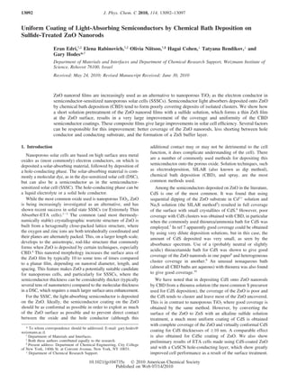
Figure 1. SEM images showing the effect of sulfide treatment on ZnO
ZnO nanowire arrays were deposited on the activated
surface coverage by CdS: (A) ZnO nanorods; (B) sulfide-treated (0.1
substrates from deposition solutions containing 0.1 M M Na2S, 10 min room temperature) ZnO; (C) CdS (deposited from an
Zn(CH3COO)2, 1.7 M (10% v/v) ethanolamine, and 0.6 M ethylenediamine/thiourea bath) on untreated ZnO; and (D) as 1C, but
ammonium hydroxide. Each substrate was immersed tilted in CdS deposited on treated ZnO. The insets show higher magnification
the deposition solution in a closed vial and heated to 90 °C in images (C and D) using backscattered images to increase the contrast
a preheated bath for 45 min. After deposition, the films were between the light atomic weight ZnO (dark) and heavier CdS (light).
rinsed with distilled water and dried in a flow of N2. In the inset of 1D (as well as in some other subsequent images in this
paper), a region where the CdS has partially peeled off (probably due
In specified experiments, ZnO was electrochemically (cath- to the cross-section fracture) was deliberately chosen to show the
odically) deposited on FTO glass from a solution of 0.05 M difference between ZnO and CdS.
zinc nitrate, at 70 °C. A standard three-electrode setup was used
with a Ag/AgCl reference electrode and a Pt foil counter
electrode. A potential of -0.9 V and a typical deposition solution concentration just before use. The samples were dipped
duration of 90 min were used. in an aqueous solution of 0.5 M LiSCN for 5 min at room
ZnO Surface Treatment. For the typical surface treatment, temperature and the excess solution was gently wiped with a
ZnO films were immersed in a solution of 0.1 M Na2S (pH ca. tissue from the surface.14 The samples were then heated on a
13) at room temperature for specific durations (see text). In some hot plate to 65-75 °C and kept at this temperature during the
cases, the ZnO was treated with solutions of 0.5 M ammonium deposition. CuSCN deposition was carried out in a homemade
sulfide (pH ca. 9.5), 0.1 M potassium hydroxide, 0.1 M apparatus using a movable syringe needle, sealed at the end
thioacetamide (40 min), or 1 M thiourea (40 min). After and with four 0.3 mm diameter holes, spaced 3 mm apart, drilled
treatment, the samples were rinsed thoroughly with deionized in the side of the needle.15 Typically 0.3-0.4 mL of solution
water. was used for a sample area of 3 cm2, resulting in a CuSCN
CdS Deposition. CdS was deposited by three different layer 1-2 µm thick above the ZnO nanorods thus preventing
chemical bath deposition solutions: thiourea/ethylenediamine contact between ZnO and the Au back contact. Gold contacts
bath (0.025 M CdAc2, 0.1 M ethylenediamine, and 0.1 M 60 nm thick were deposited on top of the CuSCN layer by
thiourea at room temperature for 30-180 min), which was the electron beam evaporation.
mostly used standard method; thiourea/ammonia bath (0.002 Film and Cell Characterization. The morphology of the
M CdSO4, 0.01 M thiourea, and 1 M ammonia), where the samples was observed by a SEM, Leo Ultra 55 scanning electron
solution was heated to 60 °C for 100 min;7 and thioacetamide microscope, in most cases using 2 kV accelerating voltage.
bath (0.01 M Cd(NO3)2 and 0.01 M thioacetamide at room XPS measurements were carried out on a Kratos AXIS
temperature for 40 min).8 After CdS deposition the samples were ULTRA system, using a monocromatized Al KR X-ray source
rinsed with deionized water and dried in a N2 flow. at 75 W and detection pass energies ranging between 20 and
CdSe Deposition. CdSe deposition was carried out by CBD 80 eV.
as described elsewhere.12 In short, stock solutions of 0.5 M The photovoltaic response of the cells was measured by using
CdSO4, 0.7 M N(CH2COOK)3 (NTA), and 0.2 M Na2SeSO3 a white-light LED lamp calibrated to give the same short circuit
(prepared by stirring 0.2 M elemental Se with 0.5 M Na2SO3 current as natural sunlight, and normalized to full sun (100
for ∼6-8 h at 70 °C) were used. The final solution composition mW · cm-2) with an Eppley pyranometer to measure the sunlight.
was 80:80:160 mM Cd:Na2SeSO3:NTA, respectively. pH was Current-voltage (I-V) measurements were made with a Kei-
adjusted to 8.5 with KOH prior to addition of selenosulfate, thley 230 programmable voltage source and a Keithley 2000
and the final pH was 10.3. The samples were placed in a stirred multimeter. A defined area of 0.91 cm2 was scribed around the
water bath at 80 °C for 30 min and subsequently were rinsed gold contact to delineate the cell size.
with deionized water and dried in a N2 flow.
CuSCN Deposition and Solar Cell Fabrication. To com- 3. Results and Discussion
plete the photovoltaic device, a CuSCN hole conductor layer The CBD ZnO rods have well-defined side faces with a
and gold contact were deposited on the samples as described rather smooth surface (Figure 1A). Attempts to grow CdS
before.13 on ZnO by a thiourea-based bath for CdS (the most common
In brief, a saturated solution of CuSCN in dipropyl sulfide type used for this technique) resulted in clustering of the
was prepared in advance by stirring the solution overnight and CdS and poor coverage of the ZnO (Figure 1C). If, however,
allowing it to settle for several days. This solution was diluted the ZnO is treated with a Na2S solution, which converts the
with dipropyl sulfide in 1:1 ratio to form 0.16 M CuSCN ZnO nanorod surface to ZnS (Figure 1B; more details on
3. 13094 J. Phys. Chem. C, Vol. 114, No. 30, 2010 Edri et al.
Figure 2. SEM images showing the effect of sulfide treatment on ZnO surface coverage by (A, B) CdS from ammonia/thiourea bath, (C, D) CdS
from a thioacetamide bath, and (E, F) CBD CdSe. Left column images (A, C, E) are nontreated ZnO rods, right column images (B, D, F) show
sulfide-treated ZnO rods. The insets are higher magnification backscattered images; scale bars for the insets are all 0.5 µm.
this reaction below), a much more even and conformal to free sulfide.16,17 Attempts to carry out the reaction in
coating by the CdS is obtained (Figure 1D). thioacetamide under alkaline conditions, to separate effects of
The method used to deposit the CdS is important. Deposition pH from thioacetamide/thiourea chemistry, resulted in almost
from a more commonly used bath (ammonia-complexed instead immediate precipitation of CdS rather than controlled deposition.
of ethylenediamine) shows the same general features as in Figure It appears that, under the conditions used for the thioacetamide
1;poor coverage on untreated ZnO and excellent coverage on CdS deposition, some partial degree of exchange of ZnO occurs
the treated ZnO (Figure 2A,B). Deposition of CdS on ZnO from to ZnS, explaining why the coverage of ZnO with CdS is
a slightly acidic thioacetamide bath has been described with better—although still inferior to coverage of the treated
good coverage found.8 In our hands, this bath gave much better ZnO—than the alkaline thiourea deposition.
coverage on untreated ZnO than did the alkaline baths (Figure We should mention a related deposition method for CdS on
2C), but a much better uniformity was obtained from the same ZnO—SILAR (Successive Ionic Layer And Reaction).5 This
bath when the ZnO was Na2S treated (Figure 2D). We note method involves successive immersion of the ZnO in solutions
that the CdS coatings in ref 8 were relatively rough compared of sulfide and Cd ions, rinsing between dips, and repeating this
with those deposited by the same method on treated ZnO (Figure process to obtain thicker films. Regardless of whether the first
2D). The effect of the ZnO treatment is not limited to CdS: immersion is in sulfide or Cd ions, the sulfide immersion will
CBD CdSe shows the same behavior, possibly even to a higher convert the ZnO surface to ZnS. The result will therefore be
degree, with extensive clustering and poor coverage for the similar to CBD on a treated ZnO surface. This explains why
untreated ZnO (Figure 2E) and very uniform coating for the the SILAR method gives a good coverage of “untreated” ZnO,
treated ZnO (2F). in contrast to CBD in general.
The difference between thioacetamide and thiourea baths in We also investigated the effect of the sulfide treatment on
terms of their covering power for untreated ZnO is not obvious. differently prepared ZnO. We used electrodeposited ZnO for
Cd ions are expected to react with both S sources faster than this purpose. Figure 3 shows CdS deposited by CBD on
Zn ions (e.g., it was shown16 for thioacetamide at pH >3 to untreated (Figure 3A) and treated (Figure 3B) electrodeposited
neutral that the reaction to form CdS had a rate constant double ZnO. Again, the effect of the treatment on the coverage of the
that for ZnS formation). The reaction of metal ions with ZnO is very pronounced.
thioacetamide to metal sulfide at pH >3 to about neutral is The time of treatment of the ZnO by the Na2S solution is not
believed to proceed by direct reaction of the metal ion and critical for obtaining good coverage. Even 30 s of treatment is
thioacetamide, rather than by hydrolysis of the thioacetamide enough for this purpose. However, it is of interest to know how
4. Sulfide-Treated ZnO Nanorods J. Phys. Chem. C, Vol. 114, No. 30, 2010 13095
Figure 3. CBD CdS on untreated (A) and treated (B) electrodeposited ZnO.
TABLE 1: ZnS Effective Thickness on ZnO As a Result of
Treatment with 0.1M Na2S at Room Temperature for
Various Timesa
time [min] thickness [Å]
0.5 3.4
1 4.0
2 5.2
5 8.2
10 12.3
20 19.5
a
Layer thickness values were derived assuming a homogeneous
and uniform layered structure. Because of the nanorod geometry, we
assume that these calculations give upper limits for the thickness
values.
Figure 4. The development of the ZnS film on ZnO by treating in
Na2S for different durations. The smooth ZnO surface is uniformly
thick the ZnS layer is, as this might be important for other covered with crystallites of ZnS until after 24 h a film of ca. 5 nm
thick ZnS covers the nanorods. Noticeable roughening develops for
purposes. For example, the ZnS, with its high bandgap and low
the thicker films, but the coverage remains excellent (we deliberately
electron affinity (therefore high-lying conduction band), might choose regions where the film has been “broken” in the process of
be a good buffer layer for solar cells using ZnO. Estimation of cross-section sample preparation to be able to measure the thickness).
the effective ZnS thickness as a function of treatment time was
made from a combination of XPS elemental analyses and SEM
images. The XPS-derived average thickness values of the ZnS
layer, shown in Table 1, were calculated by using the following ited), the CdS coating is not uniform, but rather heterogeneous.
expression (suited for a planar, uniform coating): As the deposition time increases from 10 min (top row in Figure,
5) to 30 min (bottom row), the coverage increases, as might be
expected.
d ) λ ln(1 + IZnS/IZnO)
The second conclusion is that the coverage increases as the
sulfide treatment time increases for the same CdS deposition
where d is the thickness of the ZnS layer, λ is the photoelctron time (Figure 5 going from left with no treatment, to right with
inelastic mean free path (chosen to be 2.5 nm), and IZnS and 30 min of treatment). In the absence of any treatment, no CdS
IZnO are the intensities measured for ZnS and ZnO, respectively deposit is seen after 10 min (top left image) and only very
(see the Supporting Information for more details and limits on isolated deposits after 30 min CdS (bottom left image). In
the thickness estimation). contrast, even 1 min sulfide treatment is enough to improve the
Apart from the initial rapid increase in measured thickness CdS coating drastically for both CdS deposition times (second
(and this could be due to a strong adsorption of sulfide from left images), and the coverage improves as the sulfide treatment
Na2S that is not rinsed off), the increase in ZnS thickness is time increases. Thus the ZnS layer in the treated layer not only
almost linear with treatment time up to at least 20 min. As seen improves uniformity, but also catalyzes the CdS deposition.
from a sample with 24 h treatment (ca. 5 nm ZnS, Figure 4), The sulfidation is most rapidly carried out by a sulfide
the ZnS thickness does level off. solution. Other sulfiding agents have the same effect, although
The CdS films on treated ZnO appear to be relatively slower. For good CdS coverage from 0.1 M Na2S, 30 s is
conformal, although less smooth than the untreated ZnO itself, sufficient, as already noted. However, in a 0.1 M solution of
as indeed is the treated ZnO (see the gradual roughening of the thioacetamide, 40 min is required to give a comparable effect,
surface as the sulfide treatment time increases in Figure 4). while for thiourea (1 M), a 40 min treatment decidedly improves
Deposition of thin CdS layers provides more information on the surface coverage, but to a much lesser extent than the other
the degree of coverage of the treated ZnO early in the deposition treatments. (Of course, these times will be pH dependent since
process. Since standard CdS films shown above were typically the rate of hydrolysis of the S precursors will increase with
deposited for 150 min, we also looked at 10 and 30 min increasing pH.) We find that thioacetamide reacts much faster
deposition times. The results are shown in Figure 5, where two with Cd2+ under alkaline conditions than does thiourea and
important conclusions can be drawn. The first is that, for small assume the same for Zn. Thus, as suggested earlier, the better
deposition times (i.e., relatively small amounts of CdS depos- coverage with thioacetamide (even under the mild acidic
5. 13096 J. Phys. Chem. C, Vol. 114, No. 30, 2010 Edri et al.
Figure 5. Effect of duration of sulfide treatment on ZnO surface coverage by CdS. Top row: 10 min CdS deposition after 0, 1, 10, and 30 min (left
to right, respectively) of sulfide treatment. Bottom row: the same as the top row but with 30 min of CdS CBD. Main images: Backscattered SEM.
Insets: Secondary electron images of the same regions. Scale bar (lower left image) is for all main images; for insets, the same bar represents 400
nm. The insets all show the duration of sulfide treatment (S) and CdS deposition (CdS).
conditions used) as S source instead of thiourea could be The simplest and intuitive answer is “like-to-like”: A sulfide
explained by partial sulfidation of the ZnO by the thioacetamide. (or selenide, telluride) is in general expected to grow more
Ammonium sulfide (0.5 M for 10 min) also gave comparable readily on a substrate of similar chemistry (in particular, that
results, if somewhat slower, to those of Na2S. Since the pH of has S atoms at the surface, which can bond to Cd2+ cations).
this solution is ca. 9.5 compared to ca. 13 for the Na2S solution, Another possibility that we considered is that the alkaline sulfide
this indicates that the pH of the sulfiding solution is not critical. solution “cleans” the surface. Our observation that a (non-S-
The surface treatment process is at least partially reversible. containing) alkaline solution, which actually etches the ZnO,
When ZnO rods are treated with Na2S and then annealed in air has no effect on the metal Cd chalcogenide coating of the ZnO,
at 350 °C, the rods are (rather uniformly) covered with small strongly implies that this is not the reason in our case. Since
particles, presumably due to partial (back) oxidation and slight the ZnS catalyzes the CdS deposition as noted above, the ZnS
roughening of the sulfidized surface. Nonetheless, after 30 min is clearly a better nucleation initiator than ZnO for CdS. Figure
of annealing, the surface coverage by CBD CdS is better than 5 shows that the nucleation of CdS on the ZnS/ZnO is not
that without the sulfide treatment (results not shown), although homogeneous, but occurs preferentially as bands perpendicular
not as good as unannealed, sulfided ZnO. We also note that the to the growth axes. One possibility for this could be a similar
effect did not result from simply cleaning of the ZnO surface morphology of the ZnS itself. A close look at the ZnS/ZnO
by the basic sulfide solution. Treating the ZnO in KOH solution SEM images (Figure 4) shows a slight tendency for such
(up to 0.5 M) instead of Na2S, which is expected to etch the striation of morphology for the 5 min treatment, but none for
ZnO, was not found to improve the surface coverage by CdS. the 10 min treatment. Since clear striation of the CdS occurs
While the conversion of the ZnO surface to ZnS is clearly for the 10 min treated ZnO, this suggests that the preferential
the reason for the much-improved coverage by CdS or CdSe, nucleation is not a roughness or other ZnS morphology-related
there are a number of questions that arise from our results. issue. Other possible explanations are connected with the atomic
One is: What is the mechanism of the exchange? That the level structure of the underlying ZnO (the prismatic face contains
exchange occurs is well-known and expected from simple alternating Zn and S atoms) or structural defects in the nanorods.
thermodynamical reasoning. The solubility of ZnS is ∼7 orders The ability to obtain a more conformal coverage of metal
of magnitude smaller than that of ZnO.18 Since we can expect chalcogenides on ZnO rods could have a significant impact on
exposed surface oxide to convert very rapidly to ZnS (essentially nanoporous solar cells. Here, a good contact between each
immediately on any time scale involved in the experiments in crystal of the light-absorbing semiconductor and the ZnO
this paper), a logical mechanism is one involving ionic diffusion (electron conductor) is important; clustering of the light absorber
(Zn2+ being the obvious choice) through the growing ZnS layer. crystals will increase the chances of electron-hole recombina-
The observation that the increase in ZnS thickness with reaction tion19 and will also prevent direct contact between the hole and
time decreases greatly above a few nanometers is in accord with electron conductors (which may or may not cause a problem).
this mechanism. Dissolution of ZnO and immediate reprecipi- To illustrate the importance of the sulfide treatment on the
tation of ZnS may also play a role, although this mechanism is behavior of ZnO-based solar cells, we show preliminary results
most likely during the early stages of the exchange, where there of the photovoltaic response from ZnO (CBD nanorod morphol-
is still surface oxide. ogy)/CdS/CuSCN cells (see the Experimental Section for details)
Another question to be considered is: Why does the CdS(e) comparing two cells differing only in whether the ZnO was
coverage improve when the ZnO surface is converted to ZnS? sulfide-treated or not (Figure 6).
6. Sulfide-Treated ZnO Nanorods J. Phys. Chem. C, Vol. 114, No. 30, 2010 13097
In these cells, the sulfide treatment either reduced the cell
efficiency drastically (on single crystal ZnO) or even resulted
in no appreciable photovoltaic activity at all (on planar sol-gel
films). These cells were very different from the cells described
here, and it is likely (although not certain) that the coverage of
the ZnO by the polymer was not an important issue.
4. Conclusions
We have shown that through a simple room temperature
chemical method, a uniform coverage of ZnO by chemical bath
deposited CdS and CdSe can be achieved. Dipping the ZnO
substrate in a sulfide containing solution results in partial
conversion of ZnO to ZnS, which in turn results in a uniform,
almost conformal layer of the chalcogenide film. The ZnS
Figure 6. The best J-V curves of sulfide treated (black) and nontreated
(gray) ZnO|CdS|CuSCN cells in the dark (dashed lines) and under 1 promotes nucleation of CdS compared to ZnO. This treatment
sun illumination conditions (full lines). For these cells, the ZnO has a remarkable impact on the performance of a photovoltaic
deposition solution was modified, mainly by addition of a low device (ZnO|CdS|CuSCN solar cell). Preliminary results show
concentration of an antimony salt to the deposition bath, in order to an order of magnitude improvement in solar cell efficiency.
obtain a better blocking layer under the ZnO nanorods (submitted to
Crystal Growth and Design). The modified deposition solution con- Acknowledgment. This research was supported by a research
tained: 70 mM Zn(Ac)2; 0.1 mM antimony tartrate; 0.52 M ammonium grant from Rowland and Sylvia Schaefer and by the MAGNET
hydroxide and 1.7 M ethanolamine.
programme, Office of Chief Scientist (OCS) of the Israel
Ministry of Industry & Trade & Labor.
The effect of the sulfide treatment on the performance of the
cell is very pronounced. All cell parameters are improved. In Supporting Information Available: Details of the XPS
parallel with the photovoltaic behavior, the dark diode behavior analyses of the ZnS thickness. This material is available free
of the device is improved by this treatment, as seen by the of charge via the Internet at http://pubs.acs.org.
improved rectification characteristics (the dashed lines in Figure
6). The short circuit current is increased from 0.7 to 1.7 mA/
cm2, and the open circuit voltage is increased from 180 to 490 References and Notes
mV. Also, the fill factor is improved from 34% to 44% and (1) Levy-Clement, C.; Tena-Zaera, R.; Ryan, M. A.; Katty, A.; Hodes,
consequently the efficiency is increased from 0.05% to 0.37%. G. AdV. Mater. 2005, 17, 1512.
Besides the better coverage of ZnO with the absorber, there (2) Dittrich, T.; Kieven, D.; Rusu, M.; Belaidi, A.; Tornow, J.;
Schwarzburg, K.; Lux-Steiner, M. Appl. Phys. Lett. 2008, 93, 053113-3.
are two other factors that can be favorable for photovoltaic cells. (3) Krunks, M.; Katerski, A.; Dedova, T.; Oja Acik, I.; Mere, A. Sol.
We believe that the most important one is related to the role of Energy Mater. Sol. Cells 2008, 92, 1016.
the dense ZnO layer under the ZnO nanorods. This dense (4) Govender, K.; Boyle, D. S.; Kenway, P. B.; O’Brien, P. J. Mater.
Chem. 2004, 14, 2575.
underlayer is necessary for both ZnO and TiO2 based ETA cells (5) Nicolau, Y. Appl. Surf. Sci. 1985, 22-23, 1061.
to prevent shorting between the conducting glass and the solid (6) Tak, Y.; Hong, S. J.; Lee, J. S.; Yong, K. J. Mater. Chem. 2009,
hole conductor.20 We usually find such a dense underlayer to 19, 5945.
form in situ during deposition of ZnO by our technique.11 (7) Tak, Y.; Hong, S. J.; Lee, J. S.; Yong, K. Cryst. Growth Des. 2009,
9, 2627.
However, this apparently dense layer is usually not good enough (8) Spoerke, E. D.; Lloyd, M. T.; Lee, Y.; Lambert, T. N.; McKenzie,
to prevent electrical shorting, even though it appears to be B. B.; Jiang, Y.; Olson, D. C.; Sounart, T. L.; Hsu, J. W. P.; Voigt, J. A.
structurally dense under SEM imaging; this is probably due to J. Phys. Chem. C 2009, 113, 16329.
very small cracks or pinholes in this dense layer. The sulfide (9) Wang, G.; Yang, X.; Qian, F.; Zhang, J. Z.; Li, Y. Nano Lett. 2010,
10, 1088.
treatment will allow coverage of these defects by the CBD (10) Lee, W.; Min, S. K.; Dhas, V.; Ogale, S. B.; Han, S. Electrochem.
absorber, in contrast to the poor coverage of untreated ZnO; Commun. 2009, 11, 103.
this can therefore block these defects and thus suppress shorting. (11) Kokotov, M.; Hodes, G. J. Mater. Chem. 2009, 19, 3847.
This point can explain our common observation that cells made (12) Gorer, S.; Hodes, G. J. Phys. Chem. 1994, 98, 5338.
(13) O’Regan, B.; Lenzmann, F.; Muis, R.; Wienke, J. Chem. Mater.
with untreated ZnO vary widely in performance, particularly 2002, 14, 5023.
in VOC, which will be most strongly affected by shorting, while (14) Larramona, G.; Chone, C.; Jacob, A.; Sakakura, D.; Delatouche,
cells made with treated ZnO are much more reproducible with B.; Pere, D.; Cieren, X.; Nagino, M.; Bayon, R. Chem. Mater. 2006, 18,
a much narrower spread in performance, particularly in VOC. 1688.
(15) O’Regan, B. C.; Lenzmann, F. J. Phys. Chem. B 2004, 108, 4342.
A second potential effect of the treatment is the action of the (16) Bowersox, D.; Smith, D.; Swift, E. Talanta 1960, 3, 282.
thin ZnS as a buffer layer. Buffer layers are often used in these (17) Peeters, O. M.; Blaton, N. M.; Ranter, C. J. D. J. Chem. Soc., Perkin
cells between absorber and oxide to reduce recombination.20 Trans. 2 1978, 23.
While their specific role is not well-defined, likely reasons (18) Chaparro, A. M. Chem. Mater. 2005, 17, 4118.
(19) Hodes, G. J. Phys. Chem. C 2008, 112, 17778.
include reduction of recombination of electrons in the ZnO with (20) Levy-Clement, C. In Nanostructured Materials for Solar Energy
´ ´
holes in the absorber or hole conductor by increasing electron ConVersion; Elsevier: Amsterdam, The Netherlands, 2006; pp 447-484.
hole separation and/or introduction of a potential barrier. (21) Uhlrich, J. J.; Franking, R.; Hamers, R. J.; Kuech, T. F. J. Phys.
Chem. C 2009, 113, 21147.
We note that photovoltaic cells (planar ZnO/organic polymer)
were described where (NH4)2S treatment of ZnO was used.21 JP104735C