1. A t t a c k s o n I n t e l l e c t u a l P r o p e r t y
Warren Dennis
@02693198
April 24, 2015
Advisor: Dr. Hassan Salmani
2. Dennis 2
As little as over a decade ago, the infringement of copyright would primarily pertain only
to written material, but with the vast discoveries in technology, it has also become illegal to
copyright digital content, or Intellectual Property. Everything digital, from programming codes
to processors to software are all considered intellectual properties. Reuse‐based System‐on‐Chip
(SoC) design using hardware Intellectual Property (IP) cores has become a pervasive practice in
the industry to realize bug‐free complex SoCs under aggressive time‐to‐market target. These IP
cores usually come in the form of synthesizable Register Transfer Level (RTL) descriptions (Soft
IP),or gate‐level designs directly implementable in hardware (Firm IP),or GDS‐II design
database (Hard IP). During the life‐cycle of an integrated circuit (IC), IPs are vulnerable to
various security issues including IP piracy, reverse engineering efforts to facilitate cloning,
counterfeiting, or re‐marking of ICs as well as malicious alterations by untrusted third‐party
vendors. The cost of IP infringement in the United States was estimated to be crossing $1 billion
per day in 1998 with a large contribution coming from hardware IPs. In order to derive a possible
solution, I studied the design flow of integrated circuits, the different types and functionalities of
IPs,then studies the attacks.
The design flow of IPs is very intricate and goes through severalstages before it is
packaged for commercial use. Integrated circuits are circuits made up of multiple components
such as processors,memory, peripherals that are connected on a chip or board. When designing
an integrated circuit, some questions to think about are:
What market is the Chip targeted for?
What are the Protocols involved in the Chip?
What is going to be our Processor/Bus Architectures?
What is the power/IR-drop/timing/Area/Yield/ targets and how to budget it in the Chip?
What is the process in which the Chip going to be manufactured?
What are the various third party IP's/Memory requirements?
What is our Design flow and EDA tools and methodology involved?
What is the estimated Chip Cost?
All these question are answered in the specification stage where the chip functionality is geared
toward the customers needs and if any other requirements are defined. Next would be the System
Level Design, which is broken up into three parts, the electronic system level design, Register
Level Design, and the physical design. The Electronic System Level (ESL) Design is the stage
where he user specification is created; where the user uses programming language to write the
description depending on the constraint for certain tools. The ESL ends where implementation
starts,in which implementation language can include C++, MATLAB,or VHDL. The two main
stages of the ESL are the functional design, aims at describing the systems behavior and
architectural design, aims at describing the system’s architecture in terms of the application
deployed. Also there are three design stages to consider:
Functional Design
Describing the functionality of the input/output, organization, and
behavior of each component
Application driven Design
Mapping the functional application on a platform
Meets cost and performance constraints such as processors and finding
the optimal platform
Higher level description of platform
Platform oriented Design
Delivering a virtual prototype
Fine tuning the hardware architecture
The next part of the System Level Design is Register Transfer Level, which is the stage that
3. Dennis 3
converts the user specification into RTL description, describing the interconnections of the chip
as well as the behavior. The third stage,the physical design involves deciding which logic gates
to use and where to place them. There are severalsteps that make up the physical design. They
are as follows:
Floor planning: The RTL of the
chip is assigned to gross regions of the chip,
input/output (I/O) pins are assigned and large
objects (arrays,cores, etc.) are placed.
Logic synthesis: The RTL is
mapped into a gate-level net list in the target
technology of the chip.
Placement: The gates in the net
list are assigned to no overlapping locations on the
die area.
Wavelength and
placement
Logic/placement refinement:
Iterative logical and placement transformations to
close performance and power constraints.
Clock insertion: Clock signal wiring is (commonly, clock trees) introduced into
the design.
Routing: The wires that connect the gates in the net list are added.
Post wiring optimization: Performance (timing closure), noise (signal
integrity), and yield (Design for manufacturability) violations are removed.
Design for manufacturability: The design is modified, where possible, to make
it as easy and efficient as possible to produce. This is achieved by adding
dummy metal/diffusion/poly layers wherever possible while complying with
the design rules set by the foundry.
Final checking: Since errors are expensive, time consuming and hard to spot,
extensive error checking is the rule, making sure the mapping to logic was
done correctly, and checking that the manufacturing rules were followed
faithfully.
Tapeout and mask generation: the design data is turned
into photomasks in mask data preparation.
After the chip has gone through the final checks,it is then simulated for functional verification.
This is where the user will check to see if the chip meets requirements for power, timing, and
area. For the physical check,a Design Rule Check (DRC) is done to see if the chip meets
fabrication requirements and power drops, noise and signal analysis requirements are checked.
Once passed,the chips are sent to the fabrication unit.
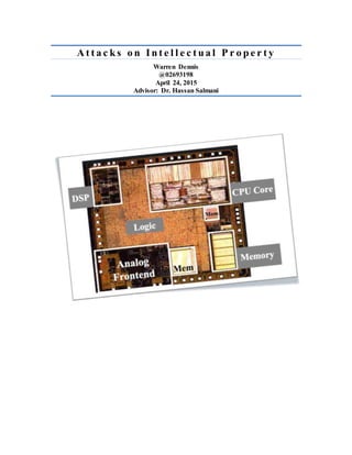
Now that we know how chips and circuits are designed, now to move on to the IP itself
and the different types and functionalities. An IP core is a reusable block of logic or data used to
make a circuit. Examples of IP could be a processor, memory, Bluetooth or Ethernet module.
Intellectual (Cunningham) properties are divided into two groups, hard and soft cores. Hard cores
are physical and are mostly used for plug and play. They are usually less portable and flexible.
Soft core IPs are the most flexible and can either exist as a schematic or a HDL code. When
severalIP cores are connected on a board, it is referred to as a System on Chip (SoC).
4. Dennis 4
The 4 methodologies when designing a SoC are:
Area-Driven Design (ADD)
Most basic and simplest methodology
Objective is to create the smallest design with most functionality
Timing-Driven Design (TDD)
Designed for meeting power consumption and performance requirements
Top down design
The floor planning and timing analysis tools can be used to determine the location of
placement sensitive areas,allowing the results to be tightly coupled into the design
optimization process.
Block-Based Design (BBD)
Driven to increase productivity and time to market by extensively using design reuse
and design hierarchy. It expands the opportunities to speed-up the delivery of
derivative products
Separates the design into two categories of activity: block authoring and block
integration. Block authoring uses a methodology which is suited to the block type
such as TDD or BBD
Block integration focuses on designing and verifying the architecture of the system
and the interfaces between the blocks
Platform-Based Design (PBD)
When manufactures produce the chips, they sign a contract that gives the consumer a certain
amount of licenses or copies of the chips, also known as chip cloning. After they are sold, there
is not a way to track them; therefore consumers are able to make more copies of the chips than
they paid for. However,it is possible for consumers to misused the IP blocks negligently because
they may have not have read the contract regarding the number of licenses for the IP core. Those
who pirate IP cores are also most likely to steala design by copying the FPGA bit stream to
configure their own products or acquire design information via reverse engineering without
paying any fees. The only way for an IP vendor to prove that their chip is being used illegally is
to obtain a sample of the product and sent it to a laboratory that specializes in reverse
engineering. To prevent reverse engineering and reduce chip cloning, a security key is stored into
5. Dennis 5
the FPGA; however, it is being stored in a volatile device.
One of the proposed solutions is to use an active security tag that contains the tag, input
data, modulation, and transmitter.
The IP tag will be used to identify the IP core that needs to be transmitted. The coding is where
the information is converted into a format more appropriate for transmission. The transmitter will
then be placed in which it will communicate with a detection equipment to allow there to be a
transfer of information. These techniques prove the illegal uses of IP cores,but do not prevent
the act of piracy.
Unfortunately, I have not found a universal solution because it the nature of the chip can be
changed. This security attack causes the manufacture companies millions of dollars as well as
their reputation.
6. Dennis 6
References
Algotronix, Carol Marsh and Tom Kean Algotronix. A Security Tagging Scheme for
ASIC Designs and Intellectual Property Cores . <http://www.design-
reuse.com/articles/15105/a-security-tagging-scheme-for-asic-designs-and-intellectual-
property-cores.html>.
Anil Deshpande, Conexant Systems Inc . Verification of IP Core Based SoC's .
<http://www.design-reuse.com/articles/18032/verification-ip-core-soc.html>.
Cunningham, Andrew. The PC inside your phone: A guide to the system-on-a-chip. 10
April 2013. <http://arstechnica.com/gadgets/2013/04/the-pc-inside-your-phone-a-guide-
to-the-system-on-a-chip/>.
Perrier, Vincent. A look inside electronic system level (ESL) design. 27 March 2004.
<http://www.eetimes.com/document.asp?doc_id=1276969>.
Rincon-Mora, Gabriel Alfonso. Analog Integrated Circuit, Why? Georgia Institute of
Technology. <http://users.ece.gatech.edu/~rincon/classes/ana_why.pdf>.
Wikipedia. Chip Design Made Easy .
<http://en.wikibooks.org/wiki/Chip_Design_Made_Easy>.
—. Integrated circuit design. <http://en.wikipedia.org/wiki/Integrated_circuit_design>.