SlideShare a Scribd company logo
1 of 39
Download to read offline
The Processor Design
• The Processor Design and Main Memory System
• CPU issues address (and data for write)
• Memory returns data for read
• Memory returns acknowledgment for write
Address
Data
Control
CPU Memory
These slides are based on the course taught by Dr. Somani at Iowa State University using
the textbook by Patterson and Hennessey titled “Computer Organization and Design.” It uses
a combination of slides provide with the teaching aids with the book and their variation
created by Dr. Somani over multiple years, before and after the adoption of the book.
• We will design a simplified MIPS processor
• The instructions supported are
– memory-reference instructions: lw, sw
– arithmetic-logical instructions: add, sub, and, or, slt
– control flow instructions: beq, j
– We will add additional instruction: bne, addi, sll, jr, jal
• Generic Implementation:
– Use program counter (PC) to point to instruction address
– Get the instruction from memory
– Read registers
– Use the instruction to decide exactly what to do
• All instructions use the ALU after reading the registers
Consider lw and sw, arithmetic/logic, control flow
Datapath & Control Design
1
2
MIPS Instruction Format
31 26 25 21 20 16 15 11 10 6 5 0
JUMP/JR/JAL JUMP ADDRESS
31 26 25 21 20 16 15 11 10 6 5 0
REG 1 REG 2
BEQ/BNE
BRANCH ADDRESS OFFSET
31 26 25 21 20 16 15 11 10 6 5 0
REG 1 REG 2
SW
STORE ADDRESS OFFSET
31 26 25 21 20 16 15 11 10 6 5 0
REG 1 REG 2
LW
LOAD ADDRESS OFFSET
31 26 25 21 20 16 15 11 10 6 5 0
REG 1 REG 2 DST
R-TYPE SHIFT AMOUNT ADD/AND/OR/SLT
31 26 25 21 20 16 15 11 10 6 5 0
REG 1 REG 2
I-TYPE
IMMEDIATE DATA
Instruction Execution
• Instruction read: PC  instruction memory, Fetch instruction
• Register read: Register numbers  register file, Read
registers
Then, depending on instruction class
• Execute: Use ALU to calculate
– Arithmetic result
– Memory address for load/store
– Branch target address
• Memory access: Access data memory for load/store
• Other Result writeback: Write data back to registers
PC update (for all): PC  target address or PC + 4
3
4
• We need an ALU
– We have already designed that
• We need memory to store instruction and data
– Instruction memory takes address and supplies instruction
– Data memory takes address and supply data for lw
– Data memory takes address and data to write into memory
• We need to manage a PC and its update mechanism
• We need a register file to include 32 registers
– We read two operands, write a result back in register file
• Sometimes part of the operand comes from instruction
• We may add support of immediate class of instructions
• We may add support for J, JR, JAL
What Blocks We Need
Simple Implementation
• Include the functional units we need for each instruction
Why do we need this stuff?
PC
Instruction
memory
Instruction
address
Instruction
a. Instructionmemory b. Programcounter
Add Sum
c. Adder
ALUcontrol
RegWrite
Registers
Write
register
Read
data1
Read
data2
Read
register 1
Read
register 2
Write
data
ALU
result
ALU
Data
Data
Register
numbers
a. Registers b. ALU
Zero
5
5
5 3
16 32
Sign
extend
b. Sign-extension unit
MemRead
MemWrite
Data
memory
Write
data
Read
data
a. Data memory unit
Address
5
6
A Review of Combinational & Sequential Circuits
Two main classes of circuits:
1. Combinational circuits
• Circuits without memory
• Outputs depend only on current input values
2. Sequential Circuits (also called Finite State Machine)
• Circuits with memory
• Memory elements to store the state of the circuit
• The state represents the input sequence in the past
• Outputs depend on both circuit state and current inputs
March 2021 Seminar series by Dr. Arun K.
Somani
7
4Mx64-bit Memory using 1Mx4 memory
4
4
15
15
15
15
4
4
14
14
14
14
4
4
13
13
13
13
4
4
12
12
12
12
4
4
11
11
11
11
4
4
10
10
10
10
4
4
9
9
9
9
4
4
8
8
8
8
4
4
7
7
7
7
4
4
6
6
6
6
4
4
5
5
5
5
4
4
4
4
4
4
4
4
3
3
3
3
4
4
2
2
2
2
4
4
1
1
1
1
4
4
0
0
0
0
B0
B1
B2
B3
Data out
Data in
24 23 22 - 13 12 - 3 2 1 0
Bank
Addr
Row Addresses Column Addresses Byte
Addr
Decoder
B3 B2 B1 B0
To select a
byte in 64 bit word
To all chips
column addresses
To all chips
row addresses
20 Addr
lines
7
8
• A memory element (flip-flop) is a one-bit storage
• A flip flop store a new bit data when a clock signal arrives.
• Clock may be a rising edge or a falling edge
• A register contains multiple flip flops, a 4-bit register is shown
• All clock signals are connected together to one clock
• Each flip-flops gets a different input
A Register
C
D Q
Q C
D Q
Q C
D Q
Q C
D Q
Q
D0 D1 D2 D3
Clock
Q0 Q1 Q2 Q3
March 2021 Seminar series by Dr. Arun K.
Somani
9
• Flip-flops also can be connected to operate as a shift register
• All clock signals are connected together to one clock
• First flip flop gets a new input
• Others get input from previous flip-flop
• A 4-bit shift register is shown below
A Shift Register
D0
C
D Q
Q C
D Q
Q C
D Q
Q C
D Q
Q
Clock
Q0 Q1 Q2 Q3
March 2021 Seminar series by Dr. Arun K.
Somani
10
9
10
A Parallel-Access Register
• We add logic to a register to create different device behaviors
• A register or shift register holds data value for one clock period
• A parallel-access register can hold data values for longer
• Alternately, it can store new data if so needed
• A LD signal enables new data or hold old data
Q3 Q2 Q1 Q0
Clock
LD
IN3 IN2 IN1 IN0
March 2021 Seminar series by Dr. Arun K.
Somani
11
• At the input of D flip-flops, a MUX is used to select whether to load
a new input or to retain the old value
• All flip-flops get the same clock cycle
• signal LD = 1 means load new value
• signal LD = 0 means retain old value
Implementation of A Parallel-Access Register
C
D Q
C
D Q
C
D Q
C
D Q
D3 D2 D1 D0
Clock
Q3 Q2 Q1 Q0
LD MUX LD MUX LD MUX LD MUX
IN0
IN3 IN2 IN1
1 0 1 0 1 0 1 0
Clock
2-to-1
MUX
IN
LD
C
D Q
P
March 2021 Seminar series by Dr. Arun K.
Somani
12
11
12
• Register file is a unit containing r (4 to 32) registers
• Each register has n (4 to 32) bits
• Output ports are used for reading the register file
– DATA1 and DATA2
– Any register can be read to any of the ports
– Each port use log2r bits to specify address
– RA1 and RA2 are read addresses
• Input port is used to write new data in register
– LD_DATA is new data
– WA (log2r bits) specifies the write address
– Writing is enabled by WR signal
A Register File
Reg
File
WA
WR
RA2
RA1
LD_DATA
DATA1
DATA2
March 2021 Seminar series by Dr. Arun K.
Somani
13
• We will design an eight-register file with 4-bit wide registers
• A single 4-bit register and its abstraction are shown below
• We need eight registers to make an eight-register file
• How many bits are required to specify a register address?
A Register File Design Details
Q3 Q2 Q1 Q0
D3 D2 D1 D0
Clock
LD
LD
Q3 Q2 Q1 Q0
D3 D2 D1 D0
Clk
LD
Q3 Q2 Q1 Q0
D3 D2 D1 D0
Clk
LD
Q3 Q2 Q1 Q0
D3 D2 D1 D0
Clk
LD
Clock
C
D Q
Q0
C
D Q
Q1
C
D Q
Q2
C
D Q
Q3
D3 D2 D1 D0
March 2021 Seminar series by Dr. Arun K.
Somani
14
13
14
• A 3-bit register address, RA, specifies which register is to be read
• For each output port, we need one 8-to-1 4-bit multiplier
Reading Circuit
7 6 5 4 3 2 1 0
8-to-1 4-bit multiplex
RA1
DATA1
7 6 5 4 3 2 1 0
8-to-1 4-bit multiplex RA2
DATA2
Q3 Q2 Q1 Q0
D3 D2 D1 D0
Clk
LD0
Q3 Q2 Q1 Q0
D3 D2 D1 D0
Clk
LD1
Q3 Q2 Q1 Q0
D3 D2 D1 D0
Clk
LD7
Register
Address
111 001 000
March 2021 Seminar series by Dr. Arun K.
Somani
15
• To write in a register, specify WA, WR signal, and new data
• A 3-bit write address is decoded if write register signal is present
• Only one of the eight registers gets a LD signal from decoder
Adding Write Control to Register File
7 6 5 4 3 2 1 0
8-to-1 4-bit multiplex
RA1
DATA1
7 6 5 4 3 2 1 0
8-to-1 4-bit multiplex RA2
DATA2
Q3 Q2 Q1 Q0
D3 D2 D1 D0
Clk
LD0
Q3 Q2 Q1 Q0
D3 D2 D1 D0
Clk
LD1
Q3 Q2 Q1 Q0
D3 D2 D1 D0
Clk
LD7
LD_DATA
WA
3
to
8
D
e
c
o
d
e
r
WR
111 001 000
LD7
LD0
LD1
LD2
March 2021 Seminar series by Dr. Arun K.
Somani
16
15
16
Arithmetic/Logic Unit
March 2021 Seminar series by Dr. Arun K.
Somani
17
4-Bit Adder
March 2021 Seminar series by Dr. Arun K.
Somani
18
17
18
4-Bit Carry-Look Ahead Adder
March 2021 Seminar series by Dr. Arun K.
Somani
19
Building A 32-bit ALU
b
0
2
Result
Operation
a
1
CarryIn
CarryOut
R e su lt31
a3 1
b3 1
R e su lt0
C arryIn
a0
b0
R e su lt1
a1
b1
R e su lt2
a2
b2
O pe ratio n
A LU 0
C arryIn
C arryO u t
A LU 1
C arryIn
C arryO u t
A LU 2
C arryIn
C arryO u t
A LU 3 1
C arryIn
March 2021 Seminar series by Dr. Arun K.
Somani
20
19
20
• A Ripple carry ALU
• Two bits decide operation
– Add/Sub
– AND
– OR
– LESS
• 1 bit decide add/sub operation
• A carry in bit
• Bit 31 generates overflow
A 32-bit ALU
March 2021 Seminar series by Dr. Arun K.
Somani
21
Test for equality
• Notice control lines:
000 = and
001 = or
010 = add
110 = subtract
111 = slt
•Note: zero is a 1
•when the result is zero!
Set
a31
0
Result0
a0
Result1
a1
0
Result2
a2
0
Operation
b31
b0
b1
b2
Result31
Overflow
Bnegate
Zero
ALU0
Less
CarryIn
CarryOut
ALU1
Less
CarryIn
CarryOut
ALU2
Less
CarryIn
CarryOut
ALU31
Less
CarryIn
March 2021 Seminar series by Dr. Arun K.
Somani
22
21
22
• Is a 32-bit ALU as fast as a 1-bit ALU?
• Is there more than one way to do addition?
– two extremes: ripple carry and sum-of-products
• Can you see the ripple? How to get rid of it?
c1 = b0c0 + a0c0 + a0b0
c2 = b1c1 + a1c1 + a1b1 c2 =
c3 = b2c2 + a2c2 + a2b2 c3 =
c4 = b3c3 + a3c3 + a3b3 c4 =
Why we can not continue this way?
Ripple Carry Adder is Slow
March 2021 Seminar series by Dr. Arun K.
Somani
23
• This is an approach in-between the two extremes
• Motivation:
– We didn't know the value of carry-in.
– Need solution.
– When would we always generate a carry? gi = ai bi
– When would we propagate the carry? pi = ai + bi
• Now all caries equations depend on p, g, and c0
c1 = g0 + p0c0
c2 = g1 + p1c1 c2 = g1+p1g0+p1p0c0
c3 = g2 + p2c2 c3 = g2+p2g1+p2p1g0+p2p1p0c0
c4 = g3 + p3c3 c4 = g3+p3g2+p3p2g1+p3p2p1g0+p3p2p1p0c0
However, this will require bigger and bigger gates.
Carry-look-ahead (CLA) adder
March 2021 Seminar series by Dr. Arun K.
Somani
24
23
24
• Generate g and p term for each bit
• Use g’s, p’s and c0 to generate all C’s
•
• Use them to generate block G and P
• CLA principle can be used recursively
A 4-bit CLA Adder
• A 16-bit adder uses
– Four 4-bit adders
• It takes block g and p terms
and cin to generate block
carry bits out
• Block carries are used to
generate bit carries
– could use ripple carry of
4-bit CLA adders
– Better: use the CLA
principle again!
Build Bigger Adders
CarryIn
Result0--3
ALU0
CarryIn
Result4--7
ALU1
CarryIn
Result8--11
ALU2
CarryIn
CarryOut
Result12--15
ALU3
CarryIn
C1
C2
C3
C4
P0
G0
P1
G1
P2
G2
P3
G3
pi
gi
pi + 1
gi + 1
ci + 1
ci + 2
ci + 3
ci + 4
pi + 2
gi + 2
pi + 3
gi + 3
a0
b0
a1
b1
a2
b2
a3
b3
a4
b4
a5
b5
a6
b6
a7
b7
a8
b8
a9
b9
a10
b10
a11
b11
a12
b12
a13
b13
a14
b14
a15
b15
Carry-lookahead unit
25
26
• 4-Bit case
– Generation of g and p: 1 gate delay
– Generation of carries (and G and P): 2 gate delay
– Generation of sum: 1 more gate delay
• 16-Bit case
– Generation of g and p: 1 gate delay
– Generation of block G and P: 2 more gate delay
– Generation of block carries: 2 more gate delay
– Generation of bit carries: 2 more gate delay
– Generation of sum: 1 more gate delay
• 64-Bit case
– 12 gate delays
CLA Adders Delay
Multiple Shift Types
MSB a[n-
1]
LSB a[0] Output out[n-1:0]
a[n-2] shiftIn Logic shift left with shiftIn
a[n-2] 0 Logic shift left
a[n-2] a[n-1] Rotate left
a[n-2] Dv Divide shift left
a[n-1] shiftIn Arithmetic shift left with shiftIn
a[n-1] 0 Arithmetic shift left
a[n-1] a[0] No shift
a[n-1] a[1] Arithmetic shift right
shiftIn a[1] Logic shift right with shiftIn
0 a[1] Logic shift right
a[0] a[1] Rotate right
ms a[1] Multiply shift right
27
28
MIPS Instruction Format
31 26 25 21 20 16 15 11 10 6 5 0
JUMP/JR/JAL JUMP ADDRESS
31 26 25 21 20 16 15 11 10 6 5 0
REG 1 REG 2
BEQ/BNE
BRANCH ADDRESS OFFSET
31 26 25 21 20 16 15 11 10 6 5 0
REG 1 REG 2
SW
STORE ADDRESS OFFSET
31 26 25 21 20 16 15 11 10 6 5 0
REG 1 REG 2
LW
LOAD ADDRESS OFFSET
31 26 25 21 20 16 15 11 10 6 5 0
REG 1 REG 2 DST
R-TYPE SHIFT AMOUNT ADD/AND/OR/SLT
31 26 25 21 20 16 15 11 10 6 5 0
REG 1 REG 2
I-TYPE
IMMEDIATE DATA
March 2021 Seminar series by Dr. Arun K.
Somani
29
Simple Implementation
• Include the functional units we need for each instruction
Why do we need this stuff?
PC
Instruction
memory
Instruction
address
Instruction
a. Instructionmemory b. Programcounter
Add Sum
c. Adder
ALUcontrol
RegW
rite
Registers
Write
register
Read
data1
Read
data2
Read
register1
Read
register2
Write
data
ALU
result
ALU
Data
Data
Register
numbers
a.Registers b. ALU
Zero
5
5
5 3
16 32
Sign
extend
b. Sign-extension unit
MemRead
MemWrite
Data
memory
Write
data
Read
data
a. Data memory unit
Address
March 2021 Seminar series by Dr. Arun K.
Somani
30
29
30
Instruction Fetch
PC register (32 bits), instruction memory, 32-bit adder (to increment PC by 4
Load/Store Instructions
• Read register operands
• Calculate address using 16-bit offset
– Use ALU, but sign-extend offset
• Load: Read memory and update register
• Store: Write register value to memory
Data memory and sign extender
ALUcontrol
RegWrite
Registers
Write
register
Read
data1
Read
data2
Read
register1
Read
register2
Write
data
ALU
result
ALU
Data
Data
Register
numbers
a. Registers b. ALU
Zero
5
5
5 3
31
32
R-Format Instructions
• Read two register operands
• Perform arithmetic/logical operation
• Write register result
Register file and ALU
Branch Instructions
33
34
• Abstract / Simplified View:
• Two types of functional units:
– elements that operate on data values (combinational)
• Example: ALU
– elements that contain state (sequential)
• Examples: Program and Data memory, Register File
Simple Implementation: Connecting Elements
Registers
Register #
Data
Register #
Data
memory
Address
Data
Register #
PC Instruction ALU
Instruction
memory
Address
CPU Overview with PC logic
Next Sequential PC = PC + 4
Branch Target
= (PC+4)+offset
A Sketchy view
An instruction changes
1. PC (all instructions, branch and jump more complex)
2. Register (arithmetic/logic, load)
3. Memory (store)
35
36
Branch Instructions
• Read register operands
• Compare operands
– Use ALU, subtract and check Zero output
• Calculate target address
– Sign-extend displacement
– Shift left 2 places (word displacement)
– Add to PC + 4
• Already calculated by instruction fetch
Making Connection: Multiplexing
 Can’t just join wires together
 Use multiplexers
37
38
Building the Datapath
• Use multiplexors to stitch them together
PC
Instruction
memory
Read
address
Instruction
16 32
Add ALU
result
M
u
x
Registers
Write
register
Write
data
Read
data 1
Read
data 2
Read
register 1
Read
register 2
Shift
left 2
4
M
u
x
ALU operation
3
RegWrite
MemRead
MemWrite
PCSrc
ALUSrc
MemtoReg
ALU
result
Zero
ALU
Data
memory
Address
Write
data
Read
data M
u
x
Sign
extend
Add
A Complete Datapath for Basic Instructions
• Lw, Sw, Add, Sub, And, Or, Slt can be performed
• For j (jump) we need an additional multiplexor
MemtoReg
MemRead
MemWrite
ALUOp
ALUSrc
RegDst
PC
Instruction
memory
Read
address
Instruction
[31–0]
Instruction [20–16]
Instruction [25–21]
Add
Instruction [5–0]
RegWrite
4
16 32
Instruction [15–0]
0
Registers
Write
register
Write
data
Write
data
Read
data 1
Read
data 2
Read
register 1
Read
register 2
Sign
extend
ALU
result
Zero
Data
memory
Address Read
data
M
u
x
1
0
M
u
x
1
0
M
u
x
1
0
M
u
x
1
Instruction [15–11]
ALU
control
Shift
left 2
PCSrc
ALU
Add
ALU
result
39
40
Control
Control signals: mux
select, read/write enable,
ALU opcode, etc.
What Else is Needed in Data Path
• Support for j and jr
– For both of them PC value comes from somewhere else
– For J, PC is created by 4 bits (31:28) from old PC, 26 bits
from IR (27:2) and 2 bits are zero (1:0)
– For JR, PC value comes from a register
• Support for JAL
– Address is same as for J inst
– OLD PC needs to be saved in register 31
• And what about immediate operand instructions
– Second operand from instruction, but without shifting
• Support for other instructions like lw and immediate inst write
41
42
• All of the logic is combinational
• We wait for everything to settle down, and the right thing to be done
– ALU might not produce “right answer” right away
– we use write signals along with clock to determine when to write
• Cycle time determined by length of the longest path
Our Simple Control Structure
We are ignoring some details like setup and hold times
Clock cycle
State
element
1
Combinational logic
State
element
2
Operation for Each Instruction
LW:
1. READ INST
2. READ REG 1
READ REG 2
3. ADD REG 1 +
OFFSET
4. READ MEM
5. WRITE REG2
SW:
1. READ INST
2. READ REG 1
READ REG 2
3. ADD REG 1 +
OFFSET
4. WRITE MEM
5.
R/I/S-Type:
1. READ INST
2. READ REG 1
READ REG 2
3. OPERATE on
REG 1 / REG 2
4.
5. WRITE DST
BR-Type:
1. READ INST
2. READ REG 1
READ REG 2
3. SUB REG 2
from REG 1
4.
5.
JMP-Type:
1. READ
INST
2.
3.
4.
5.
43
44
Data Path Operation
M
U
X
PC
Shift
Left 2
25-00
25-21
20-16
15-11
15-00
05-00
31-26
31-00
Sign
Ext
INST
MEMORY
IA
INST
4
A
D
D
DATA
MEMORY
MA
MD
WD
M
U
X
ALU
M
U
X
M
U
X
ADD
REG
FILE
RA1
RA2
RD1
RD2
WA
WD
M
U
X
ALU
CON
ALUOP
CONTROL
jmp
AND
br
zero
WE
RDES
ALU
SRC
MR MW
Memreg
Control Points
M
U
X
PC
Shift
Left 2
25-00
25-21
20-16
15-11
15-00
05-00
31-26
31-00
Sign
Ext
INST
MEMORY
IA
INST
4
A
D
D
DATA
MEMORY
MA
MD
WD
M
U
X
ALU
M
U
X
M
U
X
ADD
REG
FILE
RA1
RA2
RD1
RD2
WA
WD
M
U
X
ALU
CON
ALUOP
CONTROL
jmp
AND
br
zero
WE
RDES
ALU
SRC
MR MW
Memreg
45
46
LW Instruction Operation
M
U
X
PC
Shift
Left 2
25-00
25-21
20-16
15-11
15-00
05-00
31-26
31-00
Sign
Ext
INST
MEMORY
IA
INST
4
A
D
D
DATA
MEMORY
MA
MD
WD
M
U
X
ALU
M
U
X
M
U
X
ADD
REG
FILE
RA1
RA2
RD1
RD2
WA
WD
M
U
X
ALU
CON
ALUOP
CONTROL
jmp
AND
br
zero
WE
RDES
ALU
SRC
MR MW
Memreg
SW Instruction Operation
M
U
X
PC
Shift
Left 2
25-00
25-21
20-16
15-11
15-00
05-00
31-26
31-00
Sign
Ext
INST
MEMORY
IA
INST
4
A
D
D
DATA
MEMORY
MA
MD
WD
M
U
X
ALU
M
U
X
M
U
X
ADD
REG
FILE
RA1
RA2
RD1
RD2
WA
WD
M
U
X
ALU
CON
ALUOP
CONTROL
jmp
AND
br
zero
WE
RDES
ALU
SRC
MR MW
Memreg
47
48
R-Type Instruction Operation
M
U
X
PC
Shift
Left 2
25-00
25-21
20-16
15-11
15-00
05-00
31-26
31-00
Sign
Ext
INST
MEMORY
IA
INST
4
A
D
D
DATA
MEMORY
MA
MD
WD
M
U
X
ALU
M
U
X
M
U
X
ADD
REG
FILE
RA1
RA2
RD1
RD2
WA
WD
M
U
X
ALU
CON
ALUOP
CONTROL
jmp
AND
br
zero
WE
RDES
ALU
SRC
MR MW
Memreg
BR-Instruction Operation
M
U
X
PC
Shift
Left 2
25-00
25-21
20-16
15-11
15-00
05-00
31-26
31-00
Sign
Ext
INST
MEMORY
IA
INST
4
A
D
D
DATA
MEMORY
MA
MD
WD
M
U
X
ALU
M
U
X
M
U
X
ADD
REG
FILE
RA1
RA2
RD1
RD2
WA
WD
M
U
X
ALU
CON
ALUOP
CONTROL
jmp
AND
br
zero
WE
RDES
ALU
SRC
MR MW
Memreg
49
50
Jump Instruction Operation
M
U
X
PC
Shift
Left 2
25-00
25-21
20-16
15-11
15-00
05-00
31-26
31-00
Sign
Ext
INST
MEMORY
IA
INST
4
A
D
D
DATA
MEMORY
MA
MD
WD
M
U
X
ALU
M
U
X
M
U
X
ADD
REG
FILE
RA1
RA2
RD1
RD2
WA
WD
M
U
X
ALU
CON
ALUOP
CONTROL
jmp
AND
br
zero
WE
RDES
ALU
SRC
MR MW
Memreg
Control
• For each instruction
– Select the registers to be read (always read two)
– Select the 2nd ALU input
– Select the operation to be performed by ALU
– Select if data memory is to be read or written
– Select what is written and where in the register file
– Select what goes in PC
• Information comes from the 32 bits of the instruction
• Example:
add $8, $17, $18 Instruction Format:
•
000000 10001 10010 01000 00000 100000
op rs rt rd shamt funct
51
52
Adding Control to DataPath
Instruction RegDst ALUSrc
Memto-
Reg
Reg
Write
Mem
Read
Mem
Write Branch ALUOp1 ALUp0
R-format 1 0 0 1 0 0 0 1 0
lw 0 1 1 1 1 0 0 0 0
sw X 1 X 0 0 1 0 0 0
beq X 0 X 0 0 0 1 0 1
PC
Instruction
memory
Read
address
Instruction
[31– 0]
Instruction [20– 16]
Instruction [25– 21]
Add
Instruction [5– 0]
MemtoReg
ALUOp
MemWrite
RegWrite
MemRead
Branch
RegDst
ALUSrc
Instruction [31– 26]
4
16 32
Instruction [15– 0]
0
0
M
u
x
0
1
Control
Add ALU
result
M
u
x
0
1
Registers
Write
register
Write
data
Read
data 1
Read
data 2
Read
register 1
Read
register 2
Sign
extend
Shift
left 2
M
u
x
1
ALU
result
Zero
Data
memory
Write
data
Read
data
M
u
x
1
Instruction [15– 11]
ALU
control
ALU
Address
Summary of Control Signals
• RegDst: Write to register rt or rd?
• ALUSrc: Immediate to ALU?
• MemtoReg: Write memory or ALU output?
• RegWrite: Write to regfile at all?
• MemRead: Read from Data Memory?
• MemWrite: Write to the Data Memory?
• Branch: Is it a branch intruction?
• ALUOp[1:0]: ALU control field
53
54
• ALU's operation based on instruction type and function code
– e.g., what should the ALU do with any instruction
• Example: lw $1, 100($2)
•
35 2 1 100
op rs rt 16 bit offset
• ALU control input
000 AND
001 OR
010 add
110 subtract
111 set-on-less-than
• Why is the code for subtract 110 and not 011?
ALU Control
R-Type Instruction
55
56
R-Type: Control Signals
RegDst
ALUSrc
MemtoReg
RegWrite
MemRead
MemWrite
Branch
ALUOp[1:0]
1 (write to rd)
0 (No immediate)
0 (wrote not from memory)
1 (does write regfile)
0 (no memory read)
0 (no memory write)
0 (does write regfile)
10 (R-type ALU op)
Load Instruction
57
58
Load: Control Signals
RegDst
ALUSrc
MemtoReg
RegWrite
MemRead
MemWrite
Branch
ALUOp[1:0]
0
1
1
1
1
0
0
00
Store: Control Signals
RegDst
ALUSrc
MemtoReg
RegWrite
MemRead
MemWrite
Branch
ALUOp[1:0]
X
1
X
0
0
1
0
00
59
60
Branch-on-Equal Instruction
BEQ: Control Signals
RegDst
ALUSrc
MemtoReg
RegWrite
MemRead
MemWrite
Branch
ALUOp[1:0]
X
0
X
0
0
0
1
01
61
62
• Must describe hardware to compute 3-bit ALU conrol input
– given instruction type
00 = lw, sw
01 = beq,
10 = arithmetic
11 = Jump
– function code for arithmetic
• Control can be described using a truth table:
ALUOp
computed from instruction type
Other Control Information
ALUOp Funct field Operation
ALUOp1 ALUOp0 F5 F4 F3 F2 F1 F0
0 0 X X X X X X 010
X 1 X X X X X X 110
1 X X X 0 0 0 0 010
1 X X X 0 0 1 0 110
1 X X X 0 1 0 0 000
1 X X X 0 1 0 1 001
1 X X X 1 0 1 0 111
Implementation of Control
• Simple combinational logic to realize the truth tables
O
peration2
O
peration1
O
peration0
O
peration
A
LU
O
p1
F3
F2
F1
F0
F(5–0)
A
LU
O
p0
A
LU
O
p
A
LUcontrolblock
R-format Iw sw beq
Op0
Op1
Op2
Op3
Op4
Op5
Inputs
Outputs
RegDst
ALUSrc
MemtoReg
RegWrite
MemRead
MemWrite
Branch
ALUOp1
ALUOpO
63
64
Timing: Single Cycle Implementation
• Calculate cycle time assuming negligible delays except:
– memory (2ns), ALU and adders (2ns), register file access (1ns)
MemtoReg
MemRead
MemWrite
ALUOp
ALUSrc
RegDst
PC
Instruction
memory
Read
address
Instruction
[31– 0]
Instruction [20– 16]
Instruction [25– 21]
Add
Instruction [5– 0]
RegWrite
4
16 32
Instruction [15– 0]
0
Registers
Write
register
Write
data
Write
data
Read
data 1
Read
data 2
Read
register 1
Read
register 2
Sign
extend
ALU
result
Zero
Data
memory
Address Read
data
M
u
x
1
0
M
u
x
1
0
M
u
x
1
0
M
u
x
1
Instruction [15– 11]
ALU
control
Shift
left 2
PCSrc
ALU
Add
ALU
result
Implementing Jumps
• Jump uses word address
• Update PC with concatenation of
– Top 4 bits of old PC
– 26-bit jump address
– 00
• Need an extra control signal decoded from opcode
2 address
31:26 25:
0
Jump
65
66
Datapath With Jumps Added
Extend Single-Cycle MIPS
Consider the following instructions
• bne: branch if not equal
• jr: Jump register
• addi: add immediate
• sll: Shift left logic by a constant
• jal: Jump and link
67
68
Control Signals
• What’re the control signal values for each instruction or type?
Inst Reg-
Dst
ALU-
Src
Mem-
toReg
Reg-
Write
Mem
Read
Mem
Write
Bran
ch
ALU
Op1
ALU
Op0
Jum
p
R- 1 0 0 1 0 0 0 1 0 0
lw 0 1 1 1 1 0 0 0 0 0
sw X 1 X 0 0 1 0 0 0 0
beq X 0 X 0 0 0 1 0 1 0
j X X X 0 0 0 0 X X 1
Note: “R-” means R-format
ADDI
addi rs, rt, immediate
R[rt] = R[rs]+SignExtImm
• Read register operands (only one is used)
• Sign extend the immediate (in parallel)
• Perform arithmetic/logical operation
• Write register result
001000 rs rt immediate
31:26 25:21 20:16 15:0
69
70
ADDI Changes
What changes to this
baseline?
ADDI Datapath
71
72
ADDI Control Signals
• Like LW
– I-format instruction
– Write to register[rt]
– Use add operation
Inst Reg-
Dst
ALU-
Src
Mem-
toReg
Reg-
Write
Mem-
Read
Mem-
Write
Branc
h
ALUO
p1
ALUO
p0
R- 1 0 0 1 0 0 0 1 0
lw 0 1 1 1 1 0 0 0 0
sw X 1 X 0 0 1 0 0 0
beq X 0 X 0 0 0 1 0 1
addi 0 1 0 1 0 0 0 0 0
 Like R-format arithmetic
 Write ALU result to
register file
SLL
sll rd, rs, shamt
R[rd] = R[rt]<<shamt
• Read register operands (only one is used)
• Perform shift operation
• Write register result
Note: sllv rd, rt, rs for shift left logic variable
000000 rs rt rd shamt 000000
31:26 5:0
25:21 20:16 15:11 10:6
73
74
SLL Data Path Changes
ALU needs to do shift
75
76
JAL
jal target
PC = JumpAddr
R[31] = PC+4
• Jump uses word address
• Update PC with JumpAddr: concatenation of top 4 bits, old PC,
• 26-bit jump address, and 00 (called pseudo-direct)
• Save PC+4 to $ra
000011 address
31:26 25:0
JAL Datapath Changes?
77
78

More Related Content

Similar to PPT of Dr. Arun Somani_MIPS_SC-Extended.pdf

Basic computer organization and design
Basic computer organization and designBasic computer organization and design
Basic computer organization and designmahesh kumar prajapat
 
Arm organization and implementation
Arm organization and implementationArm organization and implementation
Arm organization and implementationShubham Singh
 
Chapter 4 the processor
Chapter 4 the processorChapter 4 the processor
Chapter 4 the processors9007912
 
Pipelining And Vector Processing
Pipelining And Vector ProcessingPipelining And Vector Processing
Pipelining And Vector ProcessingTheInnocentTuber
 
W8_1: Intro to UoS Educational Processor
W8_1: Intro to UoS Educational ProcessorW8_1: Intro to UoS Educational Processor
W8_1: Intro to UoS Educational ProcessorDaniel Roggen
 
Digital logic and microprocessors
Digital logic and microprocessorsDigital logic and microprocessors
Digital logic and microprocessorsMilind Pelagade
 
Computer Organization : CPU, Memory and I/O organization
Computer Organization : CPU, Memory and I/O organizationComputer Organization : CPU, Memory and I/O organization
Computer Organization : CPU, Memory and I/O organizationAmrutaMehata
 
POLITEKNIK MALAYSIA
POLITEKNIK MALAYSIAPOLITEKNIK MALAYSIA
POLITEKNIK MALAYSIAAiman Hud
 
Microprocessor and Microcontroller.pptx
Microprocessor and Microcontroller.pptxMicroprocessor and Microcontroller.pptx
Microprocessor and Microcontroller.pptxpvg123456
 
04 Unit IV DTE.pptx
04 Unit IV DTE.pptx04 Unit IV DTE.pptx
04 Unit IV DTE.pptxHarsheye
 
IntroductionCPU performance factorsInstruction countDeterm.docx
IntroductionCPU performance factorsInstruction countDeterm.docxIntroductionCPU performance factorsInstruction countDeterm.docx
IntroductionCPU performance factorsInstruction countDeterm.docxnormanibarber20063
 

Similar to PPT of Dr. Arun Somani_MIPS_SC-Extended.pdf (20)

Basic computer organization and design
Basic computer organization and designBasic computer organization and design
Basic computer organization and design
 
Unit iii
Unit iiiUnit iii
Unit iii
 
Digital-Unit-III.ppt
Digital-Unit-III.pptDigital-Unit-III.ppt
Digital-Unit-III.ppt
 
Unit - 5 Pipelining.pptx
Unit - 5 Pipelining.pptxUnit - 5 Pipelining.pptx
Unit - 5 Pipelining.pptx
 
Arm organization and implementation
Arm organization and implementationArm organization and implementation
Arm organization and implementation
 
Chapter 4 the processor
Chapter 4 the processorChapter 4 the processor
Chapter 4 the processor
 
Pipelining slides
Pipelining slides Pipelining slides
Pipelining slides
 
Coa.ppt2
Coa.ppt2Coa.ppt2
Coa.ppt2
 
Pipelining And Vector Processing
Pipelining And Vector ProcessingPipelining And Vector Processing
Pipelining And Vector Processing
 
W8_1: Intro to UoS Educational Processor
W8_1: Intro to UoS Educational ProcessorW8_1: Intro to UoS Educational Processor
W8_1: Intro to UoS Educational Processor
 
Digital logic and microprocessors
Digital logic and microprocessorsDigital logic and microprocessors
Digital logic and microprocessors
 
Computer Organization : CPU, Memory and I/O organization
Computer Organization : CPU, Memory and I/O organizationComputer Organization : CPU, Memory and I/O organization
Computer Organization : CPU, Memory and I/O organization
 
CO_Chapter2.ppt
CO_Chapter2.pptCO_Chapter2.ppt
CO_Chapter2.ppt
 
POLITEKNIK MALAYSIA
POLITEKNIK MALAYSIAPOLITEKNIK MALAYSIA
POLITEKNIK MALAYSIA
 
Microprocessor and Microcontroller.pptx
Microprocessor and Microcontroller.pptxMicroprocessor and Microcontroller.pptx
Microprocessor and Microcontroller.pptx
 
SUDHARSAN.V.pptx
SUDHARSAN.V.pptxSUDHARSAN.V.pptx
SUDHARSAN.V.pptx
 
04 Unit IV DTE.pptx
04 Unit IV DTE.pptx04 Unit IV DTE.pptx
04 Unit IV DTE.pptx
 
Co ppt
Co pptCo ppt
Co ppt
 
IntroductionCPU performance factorsInstruction countDeterm.docx
IntroductionCPU performance factorsInstruction countDeterm.docxIntroductionCPU performance factorsInstruction countDeterm.docx
IntroductionCPU performance factorsInstruction countDeterm.docx
 
Unit 2.1. cpu
Unit 2.1. cpuUnit 2.1. cpu
Unit 2.1. cpu
 

Recently uploaded

Boost PC performance: How more available memory can improve productivity
Boost PC performance: How more available memory can improve productivityBoost PC performance: How more available memory can improve productivity
Boost PC performance: How more available memory can improve productivityPrincipled Technologies
 
2024: Domino Containers - The Next Step. News from the Domino Container commu...
2024: Domino Containers - The Next Step. News from the Domino Container commu...2024: Domino Containers - The Next Step. News from the Domino Container commu...
2024: Domino Containers - The Next Step. News from the Domino Container commu...Martijn de Jong
 
Understanding Discord NSFW Servers A Guide for Responsible Users.pdf
Understanding Discord NSFW Servers A Guide for Responsible Users.pdfUnderstanding Discord NSFW Servers A Guide for Responsible Users.pdf
Understanding Discord NSFW Servers A Guide for Responsible Users.pdfUK Journal
 
AWS Community Day CPH - Three problems of Terraform
AWS Community Day CPH - Three problems of TerraformAWS Community Day CPH - Three problems of Terraform
AWS Community Day CPH - Three problems of TerraformAndrey Devyatkin
 
Data Cloud, More than a CDP by Matt Robison
Data Cloud, More than a CDP by Matt RobisonData Cloud, More than a CDP by Matt Robison
Data Cloud, More than a CDP by Matt RobisonAnna Loughnan Colquhoun
 
[2024]Digital Global Overview Report 2024 Meltwater.pdf
[2024]Digital Global Overview Report 2024 Meltwater.pdf[2024]Digital Global Overview Report 2024 Meltwater.pdf
[2024]Digital Global Overview Report 2024 Meltwater.pdfhans926745
 
Partners Life - Insurer Innovation Award 2024
Partners Life - Insurer Innovation Award 2024Partners Life - Insurer Innovation Award 2024
Partners Life - Insurer Innovation Award 2024The Digital Insurer
 
Real Time Object Detection Using Open CV
Real Time Object Detection Using Open CVReal Time Object Detection Using Open CV
Real Time Object Detection Using Open CVKhem
 
Workshop - Best of Both Worlds_ Combine KG and Vector search for enhanced R...
Workshop - Best of Both Worlds_ Combine  KG and Vector search for  enhanced R...Workshop - Best of Both Worlds_ Combine  KG and Vector search for  enhanced R...
Workshop - Best of Both Worlds_ Combine KG and Vector search for enhanced R...Neo4j
 
Apidays New York 2024 - Scaling API-first by Ian Reasor and Radu Cotescu, Adobe
Apidays New York 2024 - Scaling API-first by Ian Reasor and Radu Cotescu, AdobeApidays New York 2024 - Scaling API-first by Ian Reasor and Radu Cotescu, Adobe
Apidays New York 2024 - Scaling API-first by Ian Reasor and Radu Cotescu, Adobeapidays
 
ProductAnonymous-April2024-WinProductDiscovery-MelissaKlemke
ProductAnonymous-April2024-WinProductDiscovery-MelissaKlemkeProductAnonymous-April2024-WinProductDiscovery-MelissaKlemke
ProductAnonymous-April2024-WinProductDiscovery-MelissaKlemkeProduct Anonymous
 
Strategize a Smooth Tenant-to-tenant Migration and Copilot Takeoff
Strategize a Smooth Tenant-to-tenant Migration and Copilot TakeoffStrategize a Smooth Tenant-to-tenant Migration and Copilot Takeoff
Strategize a Smooth Tenant-to-tenant Migration and Copilot Takeoffsammart93
 
Tech Trends Report 2024 Future Today Institute.pdf
Tech Trends Report 2024 Future Today Institute.pdfTech Trends Report 2024 Future Today Institute.pdf
Tech Trends Report 2024 Future Today Institute.pdfhans926745
 
Scaling API-first – The story of a global engineering organization
Scaling API-first – The story of a global engineering organizationScaling API-first – The story of a global engineering organization
Scaling API-first – The story of a global engineering organizationRadu Cotescu
 
Axa Assurance Maroc - Insurer Innovation Award 2024
Axa Assurance Maroc - Insurer Innovation Award 2024Axa Assurance Maroc - Insurer Innovation Award 2024
Axa Assurance Maroc - Insurer Innovation Award 2024The Digital Insurer
 
Developing An App To Navigate The Roads of Brazil
Developing An App To Navigate The Roads of BrazilDeveloping An App To Navigate The Roads of Brazil
Developing An App To Navigate The Roads of BrazilV3cube
 
GenCyber Cyber Security Day Presentation
GenCyber Cyber Security Day PresentationGenCyber Cyber Security Day Presentation
GenCyber Cyber Security Day PresentationMichael W. Hawkins
 
Connector Corner: Accelerate revenue generation using UiPath API-centric busi...
Connector Corner: Accelerate revenue generation using UiPath API-centric busi...Connector Corner: Accelerate revenue generation using UiPath API-centric busi...
Connector Corner: Accelerate revenue generation using UiPath API-centric busi...DianaGray10
 
🐬 The future of MySQL is Postgres 🐘
🐬  The future of MySQL is Postgres   🐘🐬  The future of MySQL is Postgres   🐘
🐬 The future of MySQL is Postgres 🐘RTylerCroy
 
Driving Behavioral Change for Information Management through Data-Driven Gree...
Driving Behavioral Change for Information Management through Data-Driven Gree...Driving Behavioral Change for Information Management through Data-Driven Gree...
Driving Behavioral Change for Information Management through Data-Driven Gree...Enterprise Knowledge
 

Recently uploaded (20)

Boost PC performance: How more available memory can improve productivity
Boost PC performance: How more available memory can improve productivityBoost PC performance: How more available memory can improve productivity
Boost PC performance: How more available memory can improve productivity
 
2024: Domino Containers - The Next Step. News from the Domino Container commu...
2024: Domino Containers - The Next Step. News from the Domino Container commu...2024: Domino Containers - The Next Step. News from the Domino Container commu...
2024: Domino Containers - The Next Step. News from the Domino Container commu...
 
Understanding Discord NSFW Servers A Guide for Responsible Users.pdf
Understanding Discord NSFW Servers A Guide for Responsible Users.pdfUnderstanding Discord NSFW Servers A Guide for Responsible Users.pdf
Understanding Discord NSFW Servers A Guide for Responsible Users.pdf
 
AWS Community Day CPH - Three problems of Terraform
AWS Community Day CPH - Three problems of TerraformAWS Community Day CPH - Three problems of Terraform
AWS Community Day CPH - Three problems of Terraform
 
Data Cloud, More than a CDP by Matt Robison
Data Cloud, More than a CDP by Matt RobisonData Cloud, More than a CDP by Matt Robison
Data Cloud, More than a CDP by Matt Robison
 
[2024]Digital Global Overview Report 2024 Meltwater.pdf
[2024]Digital Global Overview Report 2024 Meltwater.pdf[2024]Digital Global Overview Report 2024 Meltwater.pdf
[2024]Digital Global Overview Report 2024 Meltwater.pdf
 
Partners Life - Insurer Innovation Award 2024
Partners Life - Insurer Innovation Award 2024Partners Life - Insurer Innovation Award 2024
Partners Life - Insurer Innovation Award 2024
 
Real Time Object Detection Using Open CV
Real Time Object Detection Using Open CVReal Time Object Detection Using Open CV
Real Time Object Detection Using Open CV
 
Workshop - Best of Both Worlds_ Combine KG and Vector search for enhanced R...
Workshop - Best of Both Worlds_ Combine  KG and Vector search for  enhanced R...Workshop - Best of Both Worlds_ Combine  KG and Vector search for  enhanced R...
Workshop - Best of Both Worlds_ Combine KG and Vector search for enhanced R...
 
Apidays New York 2024 - Scaling API-first by Ian Reasor and Radu Cotescu, Adobe
Apidays New York 2024 - Scaling API-first by Ian Reasor and Radu Cotescu, AdobeApidays New York 2024 - Scaling API-first by Ian Reasor and Radu Cotescu, Adobe
Apidays New York 2024 - Scaling API-first by Ian Reasor and Radu Cotescu, Adobe
 
ProductAnonymous-April2024-WinProductDiscovery-MelissaKlemke
ProductAnonymous-April2024-WinProductDiscovery-MelissaKlemkeProductAnonymous-April2024-WinProductDiscovery-MelissaKlemke
ProductAnonymous-April2024-WinProductDiscovery-MelissaKlemke
 
Strategize a Smooth Tenant-to-tenant Migration and Copilot Takeoff
Strategize a Smooth Tenant-to-tenant Migration and Copilot TakeoffStrategize a Smooth Tenant-to-tenant Migration and Copilot Takeoff
Strategize a Smooth Tenant-to-tenant Migration and Copilot Takeoff
 
Tech Trends Report 2024 Future Today Institute.pdf
Tech Trends Report 2024 Future Today Institute.pdfTech Trends Report 2024 Future Today Institute.pdf
Tech Trends Report 2024 Future Today Institute.pdf
 
Scaling API-first – The story of a global engineering organization
Scaling API-first – The story of a global engineering organizationScaling API-first – The story of a global engineering organization
Scaling API-first – The story of a global engineering organization
 
Axa Assurance Maroc - Insurer Innovation Award 2024
Axa Assurance Maroc - Insurer Innovation Award 2024Axa Assurance Maroc - Insurer Innovation Award 2024
Axa Assurance Maroc - Insurer Innovation Award 2024
 
Developing An App To Navigate The Roads of Brazil
Developing An App To Navigate The Roads of BrazilDeveloping An App To Navigate The Roads of Brazil
Developing An App To Navigate The Roads of Brazil
 
GenCyber Cyber Security Day Presentation
GenCyber Cyber Security Day PresentationGenCyber Cyber Security Day Presentation
GenCyber Cyber Security Day Presentation
 
Connector Corner: Accelerate revenue generation using UiPath API-centric busi...
Connector Corner: Accelerate revenue generation using UiPath API-centric busi...Connector Corner: Accelerate revenue generation using UiPath API-centric busi...
Connector Corner: Accelerate revenue generation using UiPath API-centric busi...
 
🐬 The future of MySQL is Postgres 🐘
🐬  The future of MySQL is Postgres   🐘🐬  The future of MySQL is Postgres   🐘
🐬 The future of MySQL is Postgres 🐘
 
Driving Behavioral Change for Information Management through Data-Driven Gree...
Driving Behavioral Change for Information Management through Data-Driven Gree...Driving Behavioral Change for Information Management through Data-Driven Gree...
Driving Behavioral Change for Information Management through Data-Driven Gree...
 

PPT of Dr. Arun Somani_MIPS_SC-Extended.pdf

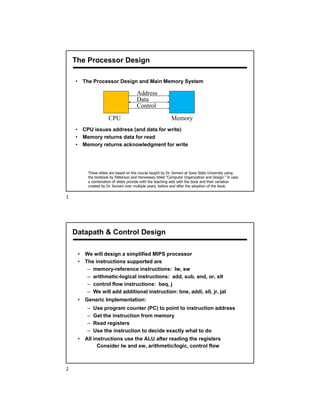
  • 1. The Processor Design • The Processor Design and Main Memory System • CPU issues address (and data for write) • Memory returns data for read • Memory returns acknowledgment for write Address Data Control CPU Memory These slides are based on the course taught by Dr. Somani at Iowa State University using the textbook by Patterson and Hennessey titled “Computer Organization and Design.” It uses a combination of slides provide with the teaching aids with the book and their variation created by Dr. Somani over multiple years, before and after the adoption of the book. • We will design a simplified MIPS processor • The instructions supported are – memory-reference instructions: lw, sw – arithmetic-logical instructions: add, sub, and, or, slt – control flow instructions: beq, j – We will add additional instruction: bne, addi, sll, jr, jal • Generic Implementation: – Use program counter (PC) to point to instruction address – Get the instruction from memory – Read registers – Use the instruction to decide exactly what to do • All instructions use the ALU after reading the registers Consider lw and sw, arithmetic/logic, control flow Datapath & Control Design 1 2
  • 2. MIPS Instruction Format 31 26 25 21 20 16 15 11 10 6 5 0 JUMP/JR/JAL JUMP ADDRESS 31 26 25 21 20 16 15 11 10 6 5 0 REG 1 REG 2 BEQ/BNE BRANCH ADDRESS OFFSET 31 26 25 21 20 16 15 11 10 6 5 0 REG 1 REG 2 SW STORE ADDRESS OFFSET 31 26 25 21 20 16 15 11 10 6 5 0 REG 1 REG 2 LW LOAD ADDRESS OFFSET 31 26 25 21 20 16 15 11 10 6 5 0 REG 1 REG 2 DST R-TYPE SHIFT AMOUNT ADD/AND/OR/SLT 31 26 25 21 20 16 15 11 10 6 5 0 REG 1 REG 2 I-TYPE IMMEDIATE DATA Instruction Execution • Instruction read: PC  instruction memory, Fetch instruction • Register read: Register numbers  register file, Read registers Then, depending on instruction class • Execute: Use ALU to calculate – Arithmetic result – Memory address for load/store – Branch target address • Memory access: Access data memory for load/store • Other Result writeback: Write data back to registers PC update (for all): PC  target address or PC + 4 3 4
  • 3. • We need an ALU – We have already designed that • We need memory to store instruction and data – Instruction memory takes address and supplies instruction – Data memory takes address and supply data for lw – Data memory takes address and data to write into memory • We need to manage a PC and its update mechanism • We need a register file to include 32 registers – We read two operands, write a result back in register file • Sometimes part of the operand comes from instruction • We may add support of immediate class of instructions • We may add support for J, JR, JAL What Blocks We Need Simple Implementation • Include the functional units we need for each instruction Why do we need this stuff? PC Instruction memory Instruction address Instruction a. Instructionmemory b. Programcounter Add Sum c. Adder ALUcontrol RegWrite Registers Write register Read data1 Read data2 Read register 1 Read register 2 Write data ALU result ALU Data Data Register numbers a. Registers b. ALU Zero 5 5 5 3 16 32 Sign extend b. Sign-extension unit MemRead MemWrite Data memory Write data Read data a. Data memory unit Address 5 6
  • 4. A Review of Combinational & Sequential Circuits Two main classes of circuits: 1. Combinational circuits • Circuits without memory • Outputs depend only on current input values 2. Sequential Circuits (also called Finite State Machine) • Circuits with memory • Memory elements to store the state of the circuit • The state represents the input sequence in the past • Outputs depend on both circuit state and current inputs March 2021 Seminar series by Dr. Arun K. Somani 7 4Mx64-bit Memory using 1Mx4 memory 4 4 15 15 15 15 4 4 14 14 14 14 4 4 13 13 13 13 4 4 12 12 12 12 4 4 11 11 11 11 4 4 10 10 10 10 4 4 9 9 9 9 4 4 8 8 8 8 4 4 7 7 7 7 4 4 6 6 6 6 4 4 5 5 5 5 4 4 4 4 4 4 4 4 3 3 3 3 4 4 2 2 2 2 4 4 1 1 1 1 4 4 0 0 0 0 B0 B1 B2 B3 Data out Data in 24 23 22 - 13 12 - 3 2 1 0 Bank Addr Row Addresses Column Addresses Byte Addr Decoder B3 B2 B1 B0 To select a byte in 64 bit word To all chips column addresses To all chips row addresses 20 Addr lines 7 8
  • 5. • A memory element (flip-flop) is a one-bit storage • A flip flop store a new bit data when a clock signal arrives. • Clock may be a rising edge or a falling edge • A register contains multiple flip flops, a 4-bit register is shown • All clock signals are connected together to one clock • Each flip-flops gets a different input A Register C D Q Q C D Q Q C D Q Q C D Q Q D0 D1 D2 D3 Clock Q0 Q1 Q2 Q3 March 2021 Seminar series by Dr. Arun K. Somani 9 • Flip-flops also can be connected to operate as a shift register • All clock signals are connected together to one clock • First flip flop gets a new input • Others get input from previous flip-flop • A 4-bit shift register is shown below A Shift Register D0 C D Q Q C D Q Q C D Q Q C D Q Q Clock Q0 Q1 Q2 Q3 March 2021 Seminar series by Dr. Arun K. Somani 10 9 10
  • 6. A Parallel-Access Register • We add logic to a register to create different device behaviors • A register or shift register holds data value for one clock period • A parallel-access register can hold data values for longer • Alternately, it can store new data if so needed • A LD signal enables new data or hold old data Q3 Q2 Q1 Q0 Clock LD IN3 IN2 IN1 IN0 March 2021 Seminar series by Dr. Arun K. Somani 11 • At the input of D flip-flops, a MUX is used to select whether to load a new input or to retain the old value • All flip-flops get the same clock cycle • signal LD = 1 means load new value • signal LD = 0 means retain old value Implementation of A Parallel-Access Register C D Q C D Q C D Q C D Q D3 D2 D1 D0 Clock Q3 Q2 Q1 Q0 LD MUX LD MUX LD MUX LD MUX IN0 IN3 IN2 IN1 1 0 1 0 1 0 1 0 Clock 2-to-1 MUX IN LD C D Q P March 2021 Seminar series by Dr. Arun K. Somani 12 11 12
  • 7. • Register file is a unit containing r (4 to 32) registers • Each register has n (4 to 32) bits • Output ports are used for reading the register file – DATA1 and DATA2 – Any register can be read to any of the ports – Each port use log2r bits to specify address – RA1 and RA2 are read addresses • Input port is used to write new data in register – LD_DATA is new data – WA (log2r bits) specifies the write address – Writing is enabled by WR signal A Register File Reg File WA WR RA2 RA1 LD_DATA DATA1 DATA2 March 2021 Seminar series by Dr. Arun K. Somani 13 • We will design an eight-register file with 4-bit wide registers • A single 4-bit register and its abstraction are shown below • We need eight registers to make an eight-register file • How many bits are required to specify a register address? A Register File Design Details Q3 Q2 Q1 Q0 D3 D2 D1 D0 Clock LD LD Q3 Q2 Q1 Q0 D3 D2 D1 D0 Clk LD Q3 Q2 Q1 Q0 D3 D2 D1 D0 Clk LD Q3 Q2 Q1 Q0 D3 D2 D1 D0 Clk LD Clock C D Q Q0 C D Q Q1 C D Q Q2 C D Q Q3 D3 D2 D1 D0 March 2021 Seminar series by Dr. Arun K. Somani 14 13 14
  • 8. • A 3-bit register address, RA, specifies which register is to be read • For each output port, we need one 8-to-1 4-bit multiplier Reading Circuit 7 6 5 4 3 2 1 0 8-to-1 4-bit multiplex RA1 DATA1 7 6 5 4 3 2 1 0 8-to-1 4-bit multiplex RA2 DATA2 Q3 Q2 Q1 Q0 D3 D2 D1 D0 Clk LD0 Q3 Q2 Q1 Q0 D3 D2 D1 D0 Clk LD1 Q3 Q2 Q1 Q0 D3 D2 D1 D0 Clk LD7 Register Address 111 001 000 March 2021 Seminar series by Dr. Arun K. Somani 15 • To write in a register, specify WA, WR signal, and new data • A 3-bit write address is decoded if write register signal is present • Only one of the eight registers gets a LD signal from decoder Adding Write Control to Register File 7 6 5 4 3 2 1 0 8-to-1 4-bit multiplex RA1 DATA1 7 6 5 4 3 2 1 0 8-to-1 4-bit multiplex RA2 DATA2 Q3 Q2 Q1 Q0 D3 D2 D1 D0 Clk LD0 Q3 Q2 Q1 Q0 D3 D2 D1 D0 Clk LD1 Q3 Q2 Q1 Q0 D3 D2 D1 D0 Clk LD7 LD_DATA WA 3 to 8 D e c o d e r WR 111 001 000 LD7 LD0 LD1 LD2 March 2021 Seminar series by Dr. Arun K. Somani 16 15 16
  • 9. Arithmetic/Logic Unit March 2021 Seminar series by Dr. Arun K. Somani 17 4-Bit Adder March 2021 Seminar series by Dr. Arun K. Somani 18 17 18
  • 10. 4-Bit Carry-Look Ahead Adder March 2021 Seminar series by Dr. Arun K. Somani 19 Building A 32-bit ALU b 0 2 Result Operation a 1 CarryIn CarryOut R e su lt31 a3 1 b3 1 R e su lt0 C arryIn a0 b0 R e su lt1 a1 b1 R e su lt2 a2 b2 O pe ratio n A LU 0 C arryIn C arryO u t A LU 1 C arryIn C arryO u t A LU 2 C arryIn C arryO u t A LU 3 1 C arryIn March 2021 Seminar series by Dr. Arun K. Somani 20 19 20
  • 11. • A Ripple carry ALU • Two bits decide operation – Add/Sub – AND – OR – LESS • 1 bit decide add/sub operation • A carry in bit • Bit 31 generates overflow A 32-bit ALU March 2021 Seminar series by Dr. Arun K. Somani 21 Test for equality • Notice control lines: 000 = and 001 = or 010 = add 110 = subtract 111 = slt •Note: zero is a 1 •when the result is zero! Set a31 0 Result0 a0 Result1 a1 0 Result2 a2 0 Operation b31 b0 b1 b2 Result31 Overflow Bnegate Zero ALU0 Less CarryIn CarryOut ALU1 Less CarryIn CarryOut ALU2 Less CarryIn CarryOut ALU31 Less CarryIn March 2021 Seminar series by Dr. Arun K. Somani 22 21 22
  • 12. • Is a 32-bit ALU as fast as a 1-bit ALU? • Is there more than one way to do addition? – two extremes: ripple carry and sum-of-products • Can you see the ripple? How to get rid of it? c1 = b0c0 + a0c0 + a0b0 c2 = b1c1 + a1c1 + a1b1 c2 = c3 = b2c2 + a2c2 + a2b2 c3 = c4 = b3c3 + a3c3 + a3b3 c4 = Why we can not continue this way? Ripple Carry Adder is Slow March 2021 Seminar series by Dr. Arun K. Somani 23 • This is an approach in-between the two extremes • Motivation: – We didn't know the value of carry-in. – Need solution. – When would we always generate a carry? gi = ai bi – When would we propagate the carry? pi = ai + bi • Now all caries equations depend on p, g, and c0 c1 = g0 + p0c0 c2 = g1 + p1c1 c2 = g1+p1g0+p1p0c0 c3 = g2 + p2c2 c3 = g2+p2g1+p2p1g0+p2p1p0c0 c4 = g3 + p3c3 c4 = g3+p3g2+p3p2g1+p3p2p1g0+p3p2p1p0c0 However, this will require bigger and bigger gates. Carry-look-ahead (CLA) adder March 2021 Seminar series by Dr. Arun K. Somani 24 23 24
  • 13. • Generate g and p term for each bit • Use g’s, p’s and c0 to generate all C’s • • Use them to generate block G and P • CLA principle can be used recursively A 4-bit CLA Adder • A 16-bit adder uses – Four 4-bit adders • It takes block g and p terms and cin to generate block carry bits out • Block carries are used to generate bit carries – could use ripple carry of 4-bit CLA adders – Better: use the CLA principle again! Build Bigger Adders CarryIn Result0--3 ALU0 CarryIn Result4--7 ALU1 CarryIn Result8--11 ALU2 CarryIn CarryOut Result12--15 ALU3 CarryIn C1 C2 C3 C4 P0 G0 P1 G1 P2 G2 P3 G3 pi gi pi + 1 gi + 1 ci + 1 ci + 2 ci + 3 ci + 4 pi + 2 gi + 2 pi + 3 gi + 3 a0 b0 a1 b1 a2 b2 a3 b3 a4 b4 a5 b5 a6 b6 a7 b7 a8 b8 a9 b9 a10 b10 a11 b11 a12 b12 a13 b13 a14 b14 a15 b15 Carry-lookahead unit 25 26
  • 14. • 4-Bit case – Generation of g and p: 1 gate delay – Generation of carries (and G and P): 2 gate delay – Generation of sum: 1 more gate delay • 16-Bit case – Generation of g and p: 1 gate delay – Generation of block G and P: 2 more gate delay – Generation of block carries: 2 more gate delay – Generation of bit carries: 2 more gate delay – Generation of sum: 1 more gate delay • 64-Bit case – 12 gate delays CLA Adders Delay Multiple Shift Types MSB a[n- 1] LSB a[0] Output out[n-1:0] a[n-2] shiftIn Logic shift left with shiftIn a[n-2] 0 Logic shift left a[n-2] a[n-1] Rotate left a[n-2] Dv Divide shift left a[n-1] shiftIn Arithmetic shift left with shiftIn a[n-1] 0 Arithmetic shift left a[n-1] a[0] No shift a[n-1] a[1] Arithmetic shift right shiftIn a[1] Logic shift right with shiftIn 0 a[1] Logic shift right a[0] a[1] Rotate right ms a[1] Multiply shift right 27 28
  • 15. MIPS Instruction Format 31 26 25 21 20 16 15 11 10 6 5 0 JUMP/JR/JAL JUMP ADDRESS 31 26 25 21 20 16 15 11 10 6 5 0 REG 1 REG 2 BEQ/BNE BRANCH ADDRESS OFFSET 31 26 25 21 20 16 15 11 10 6 5 0 REG 1 REG 2 SW STORE ADDRESS OFFSET 31 26 25 21 20 16 15 11 10 6 5 0 REG 1 REG 2 LW LOAD ADDRESS OFFSET 31 26 25 21 20 16 15 11 10 6 5 0 REG 1 REG 2 DST R-TYPE SHIFT AMOUNT ADD/AND/OR/SLT 31 26 25 21 20 16 15 11 10 6 5 0 REG 1 REG 2 I-TYPE IMMEDIATE DATA March 2021 Seminar series by Dr. Arun K. Somani 29 Simple Implementation • Include the functional units we need for each instruction Why do we need this stuff? PC Instruction memory Instruction address Instruction a. Instructionmemory b. Programcounter Add Sum c. Adder ALUcontrol RegW rite Registers Write register Read data1 Read data2 Read register1 Read register2 Write data ALU result ALU Data Data Register numbers a.Registers b. ALU Zero 5 5 5 3 16 32 Sign extend b. Sign-extension unit MemRead MemWrite Data memory Write data Read data a. Data memory unit Address March 2021 Seminar series by Dr. Arun K. Somani 30 29 30
  • 16. Instruction Fetch PC register (32 bits), instruction memory, 32-bit adder (to increment PC by 4 Load/Store Instructions • Read register operands • Calculate address using 16-bit offset – Use ALU, but sign-extend offset • Load: Read memory and update register • Store: Write register value to memory Data memory and sign extender ALUcontrol RegWrite Registers Write register Read data1 Read data2 Read register1 Read register2 Write data ALU result ALU Data Data Register numbers a. Registers b. ALU Zero 5 5 5 3 31 32
  • 17. R-Format Instructions • Read two register operands • Perform arithmetic/logical operation • Write register result Register file and ALU Branch Instructions 33 34
  • 18. • Abstract / Simplified View: • Two types of functional units: – elements that operate on data values (combinational) • Example: ALU – elements that contain state (sequential) • Examples: Program and Data memory, Register File Simple Implementation: Connecting Elements Registers Register # Data Register # Data memory Address Data Register # PC Instruction ALU Instruction memory Address CPU Overview with PC logic Next Sequential PC = PC + 4 Branch Target = (PC+4)+offset A Sketchy view An instruction changes 1. PC (all instructions, branch and jump more complex) 2. Register (arithmetic/logic, load) 3. Memory (store) 35 36
  • 19. Branch Instructions • Read register operands • Compare operands – Use ALU, subtract and check Zero output • Calculate target address – Sign-extend displacement – Shift left 2 places (word displacement) – Add to PC + 4 • Already calculated by instruction fetch Making Connection: Multiplexing  Can’t just join wires together  Use multiplexers 37 38
  • 20. Building the Datapath • Use multiplexors to stitch them together PC Instruction memory Read address Instruction 16 32 Add ALU result M u x Registers Write register Write data Read data 1 Read data 2 Read register 1 Read register 2 Shift left 2 4 M u x ALU operation 3 RegWrite MemRead MemWrite PCSrc ALUSrc MemtoReg ALU result Zero ALU Data memory Address Write data Read data M u x Sign extend Add A Complete Datapath for Basic Instructions • Lw, Sw, Add, Sub, And, Or, Slt can be performed • For j (jump) we need an additional multiplexor MemtoReg MemRead MemWrite ALUOp ALUSrc RegDst PC Instruction memory Read address Instruction [31–0] Instruction [20–16] Instruction [25–21] Add Instruction [5–0] RegWrite 4 16 32 Instruction [15–0] 0 Registers Write register Write data Write data Read data 1 Read data 2 Read register 1 Read register 2 Sign extend ALU result Zero Data memory Address Read data M u x 1 0 M u x 1 0 M u x 1 0 M u x 1 Instruction [15–11] ALU control Shift left 2 PCSrc ALU Add ALU result 39 40
  • 21. Control Control signals: mux select, read/write enable, ALU opcode, etc. What Else is Needed in Data Path • Support for j and jr – For both of them PC value comes from somewhere else – For J, PC is created by 4 bits (31:28) from old PC, 26 bits from IR (27:2) and 2 bits are zero (1:0) – For JR, PC value comes from a register • Support for JAL – Address is same as for J inst – OLD PC needs to be saved in register 31 • And what about immediate operand instructions – Second operand from instruction, but without shifting • Support for other instructions like lw and immediate inst write 41 42
  • 22. • All of the logic is combinational • We wait for everything to settle down, and the right thing to be done – ALU might not produce “right answer” right away – we use write signals along with clock to determine when to write • Cycle time determined by length of the longest path Our Simple Control Structure We are ignoring some details like setup and hold times Clock cycle State element 1 Combinational logic State element 2 Operation for Each Instruction LW: 1. READ INST 2. READ REG 1 READ REG 2 3. ADD REG 1 + OFFSET 4. READ MEM 5. WRITE REG2 SW: 1. READ INST 2. READ REG 1 READ REG 2 3. ADD REG 1 + OFFSET 4. WRITE MEM 5. R/I/S-Type: 1. READ INST 2. READ REG 1 READ REG 2 3. OPERATE on REG 1 / REG 2 4. 5. WRITE DST BR-Type: 1. READ INST 2. READ REG 1 READ REG 2 3. SUB REG 2 from REG 1 4. 5. JMP-Type: 1. READ INST 2. 3. 4. 5. 43 44
  • 23. Data Path Operation M U X PC Shift Left 2 25-00 25-21 20-16 15-11 15-00 05-00 31-26 31-00 Sign Ext INST MEMORY IA INST 4 A D D DATA MEMORY MA MD WD M U X ALU M U X M U X ADD REG FILE RA1 RA2 RD1 RD2 WA WD M U X ALU CON ALUOP CONTROL jmp AND br zero WE RDES ALU SRC MR MW Memreg Control Points M U X PC Shift Left 2 25-00 25-21 20-16 15-11 15-00 05-00 31-26 31-00 Sign Ext INST MEMORY IA INST 4 A D D DATA MEMORY MA MD WD M U X ALU M U X M U X ADD REG FILE RA1 RA2 RD1 RD2 WA WD M U X ALU CON ALUOP CONTROL jmp AND br zero WE RDES ALU SRC MR MW Memreg 45 46
  • 24. LW Instruction Operation M U X PC Shift Left 2 25-00 25-21 20-16 15-11 15-00 05-00 31-26 31-00 Sign Ext INST MEMORY IA INST 4 A D D DATA MEMORY MA MD WD M U X ALU M U X M U X ADD REG FILE RA1 RA2 RD1 RD2 WA WD M U X ALU CON ALUOP CONTROL jmp AND br zero WE RDES ALU SRC MR MW Memreg SW Instruction Operation M U X PC Shift Left 2 25-00 25-21 20-16 15-11 15-00 05-00 31-26 31-00 Sign Ext INST MEMORY IA INST 4 A D D DATA MEMORY MA MD WD M U X ALU M U X M U X ADD REG FILE RA1 RA2 RD1 RD2 WA WD M U X ALU CON ALUOP CONTROL jmp AND br zero WE RDES ALU SRC MR MW Memreg 47 48
  • 25. R-Type Instruction Operation M U X PC Shift Left 2 25-00 25-21 20-16 15-11 15-00 05-00 31-26 31-00 Sign Ext INST MEMORY IA INST 4 A D D DATA MEMORY MA MD WD M U X ALU M U X M U X ADD REG FILE RA1 RA2 RD1 RD2 WA WD M U X ALU CON ALUOP CONTROL jmp AND br zero WE RDES ALU SRC MR MW Memreg BR-Instruction Operation M U X PC Shift Left 2 25-00 25-21 20-16 15-11 15-00 05-00 31-26 31-00 Sign Ext INST MEMORY IA INST 4 A D D DATA MEMORY MA MD WD M U X ALU M U X M U X ADD REG FILE RA1 RA2 RD1 RD2 WA WD M U X ALU CON ALUOP CONTROL jmp AND br zero WE RDES ALU SRC MR MW Memreg 49 50
  • 26. Jump Instruction Operation M U X PC Shift Left 2 25-00 25-21 20-16 15-11 15-00 05-00 31-26 31-00 Sign Ext INST MEMORY IA INST 4 A D D DATA MEMORY MA MD WD M U X ALU M U X M U X ADD REG FILE RA1 RA2 RD1 RD2 WA WD M U X ALU CON ALUOP CONTROL jmp AND br zero WE RDES ALU SRC MR MW Memreg Control • For each instruction – Select the registers to be read (always read two) – Select the 2nd ALU input – Select the operation to be performed by ALU – Select if data memory is to be read or written – Select what is written and where in the register file – Select what goes in PC • Information comes from the 32 bits of the instruction • Example: add $8, $17, $18 Instruction Format: • 000000 10001 10010 01000 00000 100000 op rs rt rd shamt funct 51 52
  • 27. Adding Control to DataPath Instruction RegDst ALUSrc Memto- Reg Reg Write Mem Read Mem Write Branch ALUOp1 ALUp0 R-format 1 0 0 1 0 0 0 1 0 lw 0 1 1 1 1 0 0 0 0 sw X 1 X 0 0 1 0 0 0 beq X 0 X 0 0 0 1 0 1 PC Instruction memory Read address Instruction [31– 0] Instruction [20– 16] Instruction [25– 21] Add Instruction [5– 0] MemtoReg ALUOp MemWrite RegWrite MemRead Branch RegDst ALUSrc Instruction [31– 26] 4 16 32 Instruction [15– 0] 0 0 M u x 0 1 Control Add ALU result M u x 0 1 Registers Write register Write data Read data 1 Read data 2 Read register 1 Read register 2 Sign extend Shift left 2 M u x 1 ALU result Zero Data memory Write data Read data M u x 1 Instruction [15– 11] ALU control ALU Address Summary of Control Signals • RegDst: Write to register rt or rd? • ALUSrc: Immediate to ALU? • MemtoReg: Write memory or ALU output? • RegWrite: Write to regfile at all? • MemRead: Read from Data Memory? • MemWrite: Write to the Data Memory? • Branch: Is it a branch intruction? • ALUOp[1:0]: ALU control field 53 54
  • 28. • ALU's operation based on instruction type and function code – e.g., what should the ALU do with any instruction • Example: lw $1, 100($2) • 35 2 1 100 op rs rt 16 bit offset • ALU control input 000 AND 001 OR 010 add 110 subtract 111 set-on-less-than • Why is the code for subtract 110 and not 011? ALU Control R-Type Instruction 55 56
  • 29. R-Type: Control Signals RegDst ALUSrc MemtoReg RegWrite MemRead MemWrite Branch ALUOp[1:0] 1 (write to rd) 0 (No immediate) 0 (wrote not from memory) 1 (does write regfile) 0 (no memory read) 0 (no memory write) 0 (does write regfile) 10 (R-type ALU op) Load Instruction 57 58
  • 30. Load: Control Signals RegDst ALUSrc MemtoReg RegWrite MemRead MemWrite Branch ALUOp[1:0] 0 1 1 1 1 0 0 00 Store: Control Signals RegDst ALUSrc MemtoReg RegWrite MemRead MemWrite Branch ALUOp[1:0] X 1 X 0 0 1 0 00 59 60
  • 31. Branch-on-Equal Instruction BEQ: Control Signals RegDst ALUSrc MemtoReg RegWrite MemRead MemWrite Branch ALUOp[1:0] X 0 X 0 0 0 1 01 61 62
  • 32. • Must describe hardware to compute 3-bit ALU conrol input – given instruction type 00 = lw, sw 01 = beq, 10 = arithmetic 11 = Jump – function code for arithmetic • Control can be described using a truth table: ALUOp computed from instruction type Other Control Information ALUOp Funct field Operation ALUOp1 ALUOp0 F5 F4 F3 F2 F1 F0 0 0 X X X X X X 010 X 1 X X X X X X 110 1 X X X 0 0 0 0 010 1 X X X 0 0 1 0 110 1 X X X 0 1 0 0 000 1 X X X 0 1 0 1 001 1 X X X 1 0 1 0 111 Implementation of Control • Simple combinational logic to realize the truth tables O peration2 O peration1 O peration0 O peration A LU O p1 F3 F2 F1 F0 F(5–0) A LU O p0 A LU O p A LUcontrolblock R-format Iw sw beq Op0 Op1 Op2 Op3 Op4 Op5 Inputs Outputs RegDst ALUSrc MemtoReg RegWrite MemRead MemWrite Branch ALUOp1 ALUOpO 63 64
  • 33. Timing: Single Cycle Implementation • Calculate cycle time assuming negligible delays except: – memory (2ns), ALU and adders (2ns), register file access (1ns) MemtoReg MemRead MemWrite ALUOp ALUSrc RegDst PC Instruction memory Read address Instruction [31– 0] Instruction [20– 16] Instruction [25– 21] Add Instruction [5– 0] RegWrite 4 16 32 Instruction [15– 0] 0 Registers Write register Write data Write data Read data 1 Read data 2 Read register 1 Read register 2 Sign extend ALU result Zero Data memory Address Read data M u x 1 0 M u x 1 0 M u x 1 0 M u x 1 Instruction [15– 11] ALU control Shift left 2 PCSrc ALU Add ALU result Implementing Jumps • Jump uses word address • Update PC with concatenation of – Top 4 bits of old PC – 26-bit jump address – 00 • Need an extra control signal decoded from opcode 2 address 31:26 25: 0 Jump 65 66
  • 34. Datapath With Jumps Added Extend Single-Cycle MIPS Consider the following instructions • bne: branch if not equal • jr: Jump register • addi: add immediate • sll: Shift left logic by a constant • jal: Jump and link 67 68
  • 35. Control Signals • What’re the control signal values for each instruction or type? Inst Reg- Dst ALU- Src Mem- toReg Reg- Write Mem Read Mem Write Bran ch ALU Op1 ALU Op0 Jum p R- 1 0 0 1 0 0 0 1 0 0 lw 0 1 1 1 1 0 0 0 0 0 sw X 1 X 0 0 1 0 0 0 0 beq X 0 X 0 0 0 1 0 1 0 j X X X 0 0 0 0 X X 1 Note: “R-” means R-format ADDI addi rs, rt, immediate R[rt] = R[rs]+SignExtImm • Read register operands (only one is used) • Sign extend the immediate (in parallel) • Perform arithmetic/logical operation • Write register result 001000 rs rt immediate 31:26 25:21 20:16 15:0 69 70
  • 36. ADDI Changes What changes to this baseline? ADDI Datapath 71 72
  • 37. ADDI Control Signals • Like LW – I-format instruction – Write to register[rt] – Use add operation Inst Reg- Dst ALU- Src Mem- toReg Reg- Write Mem- Read Mem- Write Branc h ALUO p1 ALUO p0 R- 1 0 0 1 0 0 0 1 0 lw 0 1 1 1 1 0 0 0 0 sw X 1 X 0 0 1 0 0 0 beq X 0 X 0 0 0 1 0 1 addi 0 1 0 1 0 0 0 0 0  Like R-format arithmetic  Write ALU result to register file SLL sll rd, rs, shamt R[rd] = R[rt]<<shamt • Read register operands (only one is used) • Perform shift operation • Write register result Note: sllv rd, rt, rs for shift left logic variable 000000 rs rt rd shamt 000000 31:26 5:0 25:21 20:16 15:11 10:6 73 74
  • 38. SLL Data Path Changes SLL Data Path Changes ALU needs to do shift 75 76
  • 39. JAL jal target PC = JumpAddr R[31] = PC+4 • Jump uses word address • Update PC with JumpAddr: concatenation of top 4 bits, old PC, • 26-bit jump address, and 00 (called pseudo-direct) • Save PC+4 to $ra 000011 address 31:26 25:0 JAL Datapath Changes? 77 78