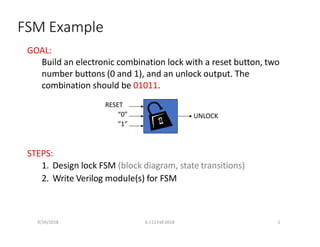
SlideShare a Scribd company logo
1 of 31
FSM Example
GOAL:
Build an electronic combination lock with a reset button, two
number buttons (0 and 1), and an unlock output. The
combination should be 01011.
RESET
“0”
“1”
9/26/2018 6.111 Fall 2018 1
UNLOCK
STEPS:
1. Design lock FSM (block diagram, state transitions)
2. Write Verilog module(s) for FSM
Step 1A: Block Diagram
fsm_clock
reset
b0_in
b1_in
lock
button
button
button
Clock
generator
Button
Reset
Button
0
Button
1
fsm
state
unlock
reset
b0
b1
LED
DISPLAY
Unlock
9/26/2018 6.111 Fall 2018 2
LED
Step 1B: State transition diagram
RESET
Unlock = 0
“0”
Unlock = 0
“01”
Unlock = 0
“01011”
Unlock = 1
“0101”
Unlock = 0
“010”
Unlock = 0
0 1
0
1
1
1 0
1
0
0
1
0
RESET
6 states  3 bits
9/26/2018 6.111 Fall 2018 3
Design Example: Level‐to‐Pulse
• A level‐to‐pulse converter produces a single‐
cycle pulse each time its input goes high.
• It’s a synchronous rising‐edge detector.
• Sample uses:
• Buttons and switches pressed by humans for
arbitrary periods of time
• Single‐cycle enable signals for counters
L
Level to
Pulse P
Converter
CLK
Whenever input L goes from
low to high...
9/26/2018 6.111 Fall 2018 4
...output P produces a single
pulse, one clock period wide.
Finite State Machines
• Finite State Machines (FSMs) are a useful abstraction for
sequential circuits with centralized “states” of operation
• At each clock edge, combinational logic computes outputs
and next state as a function of inputs and present state
Combinational
Logic
Registers
Q D
CLK
inputs
+
present
state
outputs
+
next
state
n n
9/26/2018 6.111 Fall 2018 5
Two Types of FSMs
outputs
yk =fk(S)
inputs
x0...xn
Comb.
Logic
CLK
Registers
Comb.
Logic
D Q
n
present state S
n
Moore and Mealy FSMs : different output generation
•Moore FSM:
next
state
S+
inputs
x0...xn
•Mealy FSM:
S
Comb.
Logic
CLK
Comb.
Logic
D Q
Registers
S+
n
n
outputs
yk = fk(S,x0...xn)
9/26/2018 6.111 Fall 2018 6
direct combinational path!
Design Example: Level‐to‐Pulse
• A level‐to‐pulse converter produces a single‐
cycle pulse each time its input goes high.
• It’s a synchronous rising‐edge detector.
• Sample uses:
• Buttons and switches pressed by humans for
arbitrary periods of time
• Single‐cycle enable signals for counters
L
Level to
Pulse P
Converter
CLK
Whenever input L goes from
low to high...
9/26/2018 6.111 Fall 2018 7
...output P produces a single
pulse, one clock period wide.
9/26/2018 6.111 Fall 2018 8
Reminder on the Synchronizer
• Stringing several (often two or three is sufficient)
registers in series is enough to isolate an
asynchronous input from sensitive downstream
logic and registers
Handling Metastability
• Preventing metastability turns out to be an impossible problem
• High gain of digital devices makes it likely that metastable
conditions will resolve themselves quickly
• Solution to metastability: allow time for signals to stabilize
D Q
Complicated
Sequential Logic
System
Clock
How many registers are necessary?
• Depends on many design parameters (clock speed, device speeds, …)
• In 6.111, a pair of synchronization registers is sufficient
D Q D Q
Can be
metastable right
after sampling
Very unlikely to be
metastable for >1
clock cycle
Extremely unlikely to be
metastable for >2 clock
cycles
9/26/2018 6.111 Lecture 4 9
Handling Metastability
• FF2 (D‐reg2) might go a clock cycle late, but it will
almost never* go metastable
“Metastability and Synchronizers: A Tutorial”
Ran Ginosar, Technion Israel Institute of Technology
9/26/2018 6.111 Lecture 4 1
0
*almost never generally means actually
almost never (once in ten years or something)
L=0
00
Low input,
Waiting for rise
P = 0
01
Edge Detected!
P = 1
L=1
L=0
L=0
L=1
•State transition diagram is a useful FSM representation and
design aid:
Step 1: State Transition Diagram
• Block diagram of desired system:
D Q
Level to
Pulse
FSM
L P
unsynchronized
user input
Synchronizer Edge Detector
This is the output that results from
this state. (Moore or Mealy?)
11
High input,
Waiting for fall
PP==00
Binary values of states
“if L=0 at the clock edge,
then stay in state 00.”
L=1
“if L=1 at the clock edge,
then jump to state 01.”
D Q
CLK
9/26/2018 6.111 Fall 2018 11
Valid State Transition Diagrams
11
High input,
Waiting for fall
P = 0
9/26/2018 6.111 Fall 2018 12
L=1
L=0
00
Low input,
Waiting for rise
P = 0
01
Edge Detected!
P = 1
L=1
L=0
L=0
L=1
• Arcs leaving a state are mutually exclusive, i.e., for any combination input
values there’s at most one applicable arc
• Arcs leaving a state are collectively exhaustive, i.e., for any combination of
input values there’s at least one applicable arc
• So for each state: for any combination of input values there’s exactly one
applicable arc
• Often a starting state is specified
• Each state specifies values for all outputs (Moore)
9/26/2018 6.111 Fall 2018 13
Choosing State Representation
Choice #1: binary encoding
For N states, use ceil(log2N) bits to encode the state with each state
represented by a unique combination of the bits. Tradeoffs: most efficient
use of state registers, but requires more complicated combinational logic
to detect when in a particular state.
Choice #2: “one‐hot” encoding
For N states, use N bits to encode the state where the bit corresponding to
the current state is 1, all the others 0. Tradeoffs: more state registers, but
often much less combinational logic since state decoding is trivial.
Step 2: Logic Derivation
00
Low input,
Waiting for rise
P = 0
01
Edge Detected!
P = 1
L=0
11
High input,
Waiting for fall
P = 0
L=0
L=0 L=1
Current
State
In
Next
State
Out
S1 S0 L S +
1 S +
0
P
0 0 0 0 0 0
0 0 1 0 1 0
0 1 0 0 0 1
0 1 1 1 1 1
1 1 0 0 0 0
1 1 1 1 1 0
Transition diagram is readily converted to a state
transition table (just a truth table)
L=1 L=1
• Combinational logic may be derived using Karnaugh maps
0
1
0 0 0 X
0 1 1 X
0
1
0 0 0 X
1 1 1 X
S1S0
L 00 01 11 10
S1S0
L 00 01 11 10
1
for S +:
0
for S +:
0
1
0 X
1 0
S1
for P:
0 1
S0
Comb.
Logic
n
Registers
Comb.
Logic
D Q
S
n
CLK
S+
L P
1
S + =LS 0
0
S + =L
P = S1S0
9/26/2018 6.111 Fall 2018 14
Moore Level‐to‐Pulse Converter
Moore FSM circuit implementation of level‐to‐pulse converter:
outputs
yk =fk(S)
inputs
x0...xn
Comb.
Logic
CLK
Registers
Comb.
Logic
D Q
n
present state S
n
next
state
S+
D Q
1
S + =LS 0
0
S + =L
P = S1S0
P = S1S0
S0
1
CLK
0
S +
1
S +
L P
Q
D Q
S
Q
9/26/2018 6.111 Fall 2018 15
1. When L=1 and S=0, this output is
asserted immediately and until the state
transition occurs (or L changes).
2. While in state S=1 and as long as L remains at 1, this
output is asserted until next clock.
L=1 | P=0
L=1 | P=1
0
Input is low
1
Input is high
L=0 | P=0
L=0 | P=0
Design of a Mealy Level‐to‐Pulse
S
• Since outputs are determined by state and inputs, Mealy FSMs
may need fewer states than Moore FSM implementations
Comb.
Logic Registers
Comb.
Logic
D Q
S+
n
CLK
n
direct combinational path!
L
State
P
Clock
Output transitions immediately.
State transitions at the clock edge.
1
2
9/26/2018 6.111 Fall 2018 16
Mealy Level‐to‐Pulse Converter
Pres.
State
In
Next
State
Out
S L S+ P
0
0
0
1
0
1
0
1
1
1
1
0
1
0
0
0
D Q
S
CLK
S+
Mealy FSM circuit implementation of level‐to‐pulse converter:
P
L
Q
S
• FSM’s state simply remembers the previous value of L
• Circuit benefits from the Mealy FSM’s implicit single‐cycle assertion
of outputs during state transitions
0
Input is low
9/26/2018 6.111 Fall 2018 17
1
Input is high
L=1 | P=1
L=0 | P=0
L=1 | P=0
L=0 | P=0
Moore/Mealy Trade‐Offs
• How are they different?
• Moore: outputs = f( state ) only
• Mealy outputs = f( state and input )
• Mealy outputs generally occur one cycle earlier than a Moore:
Moore: delayed assertion of P Mealy: immediate assertion of P
L L
P P
Clock Clock
State[0] State
• Compared to a Moore FSM, a Mealy FSM might...
– Be more difficult to conceptualize and design
– Have fewer states
9/26/2018 6.111 Fall 2018 18
• Moore:
• Usually more states
• Each state has a particular output
• Mealy:
• Fewer states, outputs are specified on edges of diagram
• Potential Dangers:
Moore/Mealy Trade‐Offs
Really‐long combinatorial paths!
Possible cyclic logic paths
Combinatorial logic driving itself
asynchronously through really
hard‐to‐debug pathways!
9/26/2018 6.111 Fall 2018 19
9/26/2018 45
Where should CLK come from?
• Option 1: external crystal
• Stable, known frequency, typically 50% duty cycle
• Option 2: internal signals
• Option 2A: output of combinational logic
• No! If inputs to logic change, output may make several transitions
before settling to final value  several rising edges, not just one!
Hard to design away output glitches…
• Option 2B: output of a register
• Okay, but timing of CLK2 won’t line up with CLK1
D Q
CLK1
CLK2
CLK1
CMOS VLSI Design
CMOS VLSI Design 4th Ed.
20: CAMs, ROMs, and PLAs 21
Building Logic with ROMs
 Use ROM as lookup table containing truth table
– n inputs, k outputs requires 2n words x k bits
– Changing function is easy – reprogram ROM
 Finite State Machine
– n inputs, k outputs, s bits of state
– Build with 2n+s x (k+s) bit ROM and (k+s) bit reg
n
inputs
2
n
wordlines
ROM Array
k outputs
DEC
ROM
inputs outputs
state
n k
s
k
s
CMOS VLSI Design
CMOS VLSI Design 4th Ed.
20: CAMs, ROMs, and PLAs 22
Example: RoboAnt
Let’s build an Ant
Sensors: Antennae
(L,R) – 1 when in contact
Actuators: Legs
Forward step F
Ten degree turns TL, TR
Goal: make our ant smart enough to
get out of a maze
Strategy: keep right antenna on wall
(RoboAnt adapted from MIT 6.004 2002 OpenCourseWare by Ward and Terman)
L R
CMOS VLSI Design
CMOS VLSI Design 4th Ed.
20: CAMs, ROMs, and PLAs 23
Lost in space
 Action: go forward until we hit something
– Initial state
CMOS VLSI Design
CMOS VLSI Design 4th Ed.
20: CAMs, ROMs, and PLAs 24
Bonk!!!
 Action: turn left (rotate counterclockwise)
– Until we don’t touch anymore
CMOS VLSI Design
CMOS VLSI Design 4th Ed.
20: CAMs, ROMs, and PLAs 25
A little to the right
 Action: step forward and turn right a little
– Looking for wall
CMOS VLSI Design
CMOS VLSI Design 4th Ed.
20: CAMs, ROMs, and PLAs 26
Then a little to the left
 Action: step and turn left a little, until not touching
CMOS VLSI Design
CMOS VLSI Design 4th Ed.
20: CAMs, ROMs, and PLAs 27
Whoops – a corner!
 Action: step and turn right until hitting next wall
CMOS VLSI Design
CMOS VLSI Design 4th Ed.
20: CAMs, ROMs, and PLAs 28
Simplification
 Merge equivalent states where possible
CMOS VLSI Design
CMOS VLSI Design 4th Ed.
20: CAMs, ROMs, and PLAs 29
State Transition Table
S1:0 L R S1:0’ TR TL F
00 0 0 00 0 0 1
00 1 X 01 0 0 1
00 0 1 01 0 0 1
01 1 X 01 0 1 0
01 0 1 01 0 1 0
01 0 0 10 0 1 0
10 X 0 10 1 0 1
10 X 1 11 1 0 1
11 1 X 01 0 1 1
11 0 0 10 0 1 1
11 0 1 11 0 1 1
Lost
RCCW
Wall1
Wall2
CMOS VLSI Design
CMOS VLSI Design 4th Ed.
20: CAMs, ROMs, and PLAs 30
ROM Implementation
 16-word x 5 bit ROM
ROM
L, R
S1:0
TL, TR, F
S'1:0
S1
' S0
' TR'TL' F'
0000
0001
0010
0011
0100
0101
0110
0111
1000
1001
1010
1011
1100
1101
1110
1111
4:16
DEC
S1 S0 L R
CMOS VLSI Design
CMOS VLSI Design 4th Ed.
20: CAMs, ROMs, and PLAs 31
ROM Implementation
 16-word x 5 bit ROM
ROM
L, R
S1:0
TL, TR, F
S'1:0
S1
' S0
' TR'TL' F'
0000
0001
0010
0011
0100
0101
0110
0111
1000
1001
1010
1011
1100
1101
1110
1111
4:16
DEC
S1 S0 L R

More Related Content

Similar to Lecture 12.pptx

Hardware combinational
Hardware combinationalHardware combinational
Hardware combinationalDefri Tan
 
SEQUENTIAL CIRCUITS -Module 5 (1).pptx
SEQUENTIAL CIRCUITS -Module 5 (1).pptxSEQUENTIAL CIRCUITS -Module 5 (1).pptx
SEQUENTIAL CIRCUITS -Module 5 (1).pptxThanmayiKumar
 
Admission in india 2015
Admission in india 2015Admission in india 2015
Admission in india 2015Edhole.com
 
Sequential Circuit
Sequential CircuitSequential Circuit
Sequential CircuitHeman Pathak
 
Synchronous Sequential Logic Unit 4
Synchronous Sequential Logic Unit 4Synchronous Sequential Logic Unit 4
Synchronous Sequential Logic Unit 4Asif Iqbal
 
Digital Electronics Registers and Counters.pptx
Digital Electronics Registers and Counters.pptxDigital Electronics Registers and Counters.pptx
Digital Electronics Registers and Counters.pptxnavaneethakrishnanec
 
Lec15 Intro to Computer Engineering by Hsien-Hsin Sean Lee Georgia Tech -- Re...
Lec15 Intro to Computer Engineering by Hsien-Hsin Sean Lee Georgia Tech -- Re...Lec15 Intro to Computer Engineering by Hsien-Hsin Sean Lee Georgia Tech -- Re...
Lec15 Intro to Computer Engineering by Hsien-Hsin Sean Lee Georgia Tech -- Re...Hsien-Hsin Sean Lee, Ph.D.
 
Combinational Logic Concept Powerpoint Presentation
Combinational Logic Concept Powerpoint PresentationCombinational Logic Concept Powerpoint Presentation
Combinational Logic Concept Powerpoint Presentationssuser2712bb
 
Chapter 6 - Modelling and Control of Converters.pdf
Chapter 6 - Modelling and Control of Converters.pdfChapter 6 - Modelling and Control of Converters.pdf
Chapter 6 - Modelling and Control of Converters.pdfbenson215
 
Admission in india 2015
Admission in india 2015Admission in india 2015
Admission in india 2015Edhole.com
 

Similar to Lecture 12.pptx (20)

Lec9
Lec9Lec9
Lec9
 
Hardware combinational
Hardware combinationalHardware combinational
Hardware combinational
 
lec7.ppt
lec7.pptlec7.ppt
lec7.ppt
 
Ch3
Ch3Ch3
Ch3
 
Sequential circuits
Sequential circuitsSequential circuits
Sequential circuits
 
SEQUENTIAL CIRCUITS -Module 5 (1).pptx
SEQUENTIAL CIRCUITS -Module 5 (1).pptxSEQUENTIAL CIRCUITS -Module 5 (1).pptx
SEQUENTIAL CIRCUITS -Module 5 (1).pptx
 
Admission in india 2015
Admission in india 2015Admission in india 2015
Admission in india 2015
 
Sequential Circuit
Sequential CircuitSequential Circuit
Sequential Circuit
 
Synchronous Sequential Logic Unit 4
Synchronous Sequential Logic Unit 4Synchronous Sequential Logic Unit 4
Synchronous Sequential Logic Unit 4
 
ANALOG AND DIGITAL ELECTRONICS unit 5
ANALOG AND DIGITAL ELECTRONICS unit 5ANALOG AND DIGITAL ELECTRONICS unit 5
ANALOG AND DIGITAL ELECTRONICS unit 5
 
Digital Electronics Registers and Counters.pptx
Digital Electronics Registers and Counters.pptxDigital Electronics Registers and Counters.pptx
Digital Electronics Registers and Counters.pptx
 
Sequential circuits
Sequential circuitsSequential circuits
Sequential circuits
 
Lec15 Intro to Computer Engineering by Hsien-Hsin Sean Lee Georgia Tech -- Re...
Lec15 Intro to Computer Engineering by Hsien-Hsin Sean Lee Georgia Tech -- Re...Lec15 Intro to Computer Engineering by Hsien-Hsin Sean Lee Georgia Tech -- Re...
Lec15 Intro to Computer Engineering by Hsien-Hsin Sean Lee Georgia Tech -- Re...
 
Combinational Logic Concept Powerpoint Presentation
Combinational Logic Concept Powerpoint PresentationCombinational Logic Concept Powerpoint Presentation
Combinational Logic Concept Powerpoint Presentation
 
Chapter 6 - Modelling and Control of Converters.pdf
Chapter 6 - Modelling and Control of Converters.pdfChapter 6 - Modelling and Control of Converters.pdf
Chapter 6 - Modelling and Control of Converters.pdf
 
Flip & flop by Zaheer Abbas Aghani
Flip & flop by Zaheer Abbas AghaniFlip & flop by Zaheer Abbas Aghani
Flip & flop by Zaheer Abbas Aghani
 
Admission in india 2015
Admission in india 2015Admission in india 2015
Admission in india 2015
 
Chapter 6: Sequential Logic
Chapter 6: Sequential LogicChapter 6: Sequential Logic
Chapter 6: Sequential Logic
 
Logic Gate
Logic GateLogic Gate
Logic Gate
 
QC-UNIT 2.ppt
QC-UNIT 2.pptQC-UNIT 2.ppt
QC-UNIT 2.ppt
 

Recently uploaded

complete construction, environmental and economics information of biomass com...
complete construction, environmental and economics information of biomass com...complete construction, environmental and economics information of biomass com...
complete construction, environmental and economics information of biomass com...asadnawaz62
 
APPLICATIONS-AC/DC DRIVES-OPERATING CHARACTERISTICS
APPLICATIONS-AC/DC DRIVES-OPERATING CHARACTERISTICSAPPLICATIONS-AC/DC DRIVES-OPERATING CHARACTERISTICS
APPLICATIONS-AC/DC DRIVES-OPERATING CHARACTERISTICSKurinjimalarL3
 
Heart Disease Prediction using machine learning.pptx
Heart Disease Prediction using machine learning.pptxHeart Disease Prediction using machine learning.pptx
Heart Disease Prediction using machine learning.pptxPoojaBan
 
HARMONY IN THE NATURE AND EXISTENCE - Unit-IV
HARMONY IN THE NATURE AND EXISTENCE - Unit-IVHARMONY IN THE NATURE AND EXISTENCE - Unit-IV
HARMONY IN THE NATURE AND EXISTENCE - Unit-IVRajaP95
 
Decoding Kotlin - Your guide to solving the mysterious in Kotlin.pptx
Decoding Kotlin - Your guide to solving the mysterious in Kotlin.pptxDecoding Kotlin - Your guide to solving the mysterious in Kotlin.pptx
Decoding Kotlin - Your guide to solving the mysterious in Kotlin.pptxJoão Esperancinha
 
Application of Residue Theorem to evaluate real integrations.pptx
Application of Residue Theorem to evaluate real integrations.pptxApplication of Residue Theorem to evaluate real integrations.pptx
Application of Residue Theorem to evaluate real integrations.pptx959SahilShah
 
Call Us ≽ 8377877756 ≼ Call Girls In Shastri Nagar (Delhi)
Call Us ≽ 8377877756 ≼ Call Girls In Shastri Nagar (Delhi)Call Us ≽ 8377877756 ≼ Call Girls In Shastri Nagar (Delhi)
Call Us ≽ 8377877756 ≼ Call Girls In Shastri Nagar (Delhi)dollysharma2066
 
power system scada applications and uses
power system scada applications and usespower system scada applications and uses
power system scada applications and usesDevarapalliHaritha
 
chaitra-1.pptx fake news detection using machine learning
chaitra-1.pptx  fake news detection using machine learningchaitra-1.pptx  fake news detection using machine learning
chaitra-1.pptx fake news detection using machine learningmisbanausheenparvam
 
CCS355 Neural Network & Deep Learning Unit II Notes with Question bank .pdf
CCS355 Neural Network & Deep Learning Unit II Notes with Question bank .pdfCCS355 Neural Network & Deep Learning Unit II Notes with Question bank .pdf
CCS355 Neural Network & Deep Learning Unit II Notes with Question bank .pdfAsst.prof M.Gokilavani
 
Call Girls Delhi {Jodhpur} 9711199012 high profile service
Call Girls Delhi {Jodhpur} 9711199012 high profile serviceCall Girls Delhi {Jodhpur} 9711199012 high profile service
Call Girls Delhi {Jodhpur} 9711199012 high profile servicerehmti665
 
VIP Call Girls Service Hitech City Hyderabad Call +91-8250192130
VIP Call Girls Service Hitech City Hyderabad Call +91-8250192130VIP Call Girls Service Hitech City Hyderabad Call +91-8250192130
VIP Call Girls Service Hitech City Hyderabad Call +91-8250192130Suhani Kapoor
 
Oxy acetylene welding presentation note.
Oxy acetylene welding presentation note.Oxy acetylene welding presentation note.
Oxy acetylene welding presentation note.eptoze12
 
VICTOR MAESTRE RAMIREZ - Planetary Defender on NASA's Double Asteroid Redirec...
VICTOR MAESTRE RAMIREZ - Planetary Defender on NASA's Double Asteroid Redirec...VICTOR MAESTRE RAMIREZ - Planetary Defender on NASA's Double Asteroid Redirec...
VICTOR MAESTRE RAMIREZ - Planetary Defender on NASA's Double Asteroid Redirec...VICTOR MAESTRE RAMIREZ
 
Electronically Controlled suspensions system .pdf
Electronically Controlled suspensions system .pdfElectronically Controlled suspensions system .pdf
Electronically Controlled suspensions system .pdfme23b1001
 
Artificial-Intelligence-in-Electronics (K).pptx
Artificial-Intelligence-in-Electronics (K).pptxArtificial-Intelligence-in-Electronics (K).pptx
Artificial-Intelligence-in-Electronics (K).pptxbritheesh05
 

Recently uploaded (20)

Call Us -/9953056974- Call Girls In Vikaspuri-/- Delhi NCR
Call Us -/9953056974- Call Girls In Vikaspuri-/- Delhi NCRCall Us -/9953056974- Call Girls In Vikaspuri-/- Delhi NCR
Call Us -/9953056974- Call Girls In Vikaspuri-/- Delhi NCR
 
complete construction, environmental and economics information of biomass com...
complete construction, environmental and economics information of biomass com...complete construction, environmental and economics information of biomass com...
complete construction, environmental and economics information of biomass com...
 
APPLICATIONS-AC/DC DRIVES-OPERATING CHARACTERISTICS
APPLICATIONS-AC/DC DRIVES-OPERATING CHARACTERISTICSAPPLICATIONS-AC/DC DRIVES-OPERATING CHARACTERISTICS
APPLICATIONS-AC/DC DRIVES-OPERATING CHARACTERISTICS
 
Heart Disease Prediction using machine learning.pptx
Heart Disease Prediction using machine learning.pptxHeart Disease Prediction using machine learning.pptx
Heart Disease Prediction using machine learning.pptx
 
HARMONY IN THE NATURE AND EXISTENCE - Unit-IV
HARMONY IN THE NATURE AND EXISTENCE - Unit-IVHARMONY IN THE NATURE AND EXISTENCE - Unit-IV
HARMONY IN THE NATURE AND EXISTENCE - Unit-IV
 
Decoding Kotlin - Your guide to solving the mysterious in Kotlin.pptx
Decoding Kotlin - Your guide to solving the mysterious in Kotlin.pptxDecoding Kotlin - Your guide to solving the mysterious in Kotlin.pptx
Decoding Kotlin - Your guide to solving the mysterious in Kotlin.pptx
 
Application of Residue Theorem to evaluate real integrations.pptx
Application of Residue Theorem to evaluate real integrations.pptxApplication of Residue Theorem to evaluate real integrations.pptx
Application of Residue Theorem to evaluate real integrations.pptx
 
Call Us ≽ 8377877756 ≼ Call Girls In Shastri Nagar (Delhi)
Call Us ≽ 8377877756 ≼ Call Girls In Shastri Nagar (Delhi)Call Us ≽ 8377877756 ≼ Call Girls In Shastri Nagar (Delhi)
Call Us ≽ 8377877756 ≼ Call Girls In Shastri Nagar (Delhi)
 
9953056974 Call Girls In South Ex, Escorts (Delhi) NCR.pdf
9953056974 Call Girls In South Ex, Escorts (Delhi) NCR.pdf9953056974 Call Girls In South Ex, Escorts (Delhi) NCR.pdf
9953056974 Call Girls In South Ex, Escorts (Delhi) NCR.pdf
 
power system scada applications and uses
power system scada applications and usespower system scada applications and uses
power system scada applications and uses
 
chaitra-1.pptx fake news detection using machine learning
chaitra-1.pptx  fake news detection using machine learningchaitra-1.pptx  fake news detection using machine learning
chaitra-1.pptx fake news detection using machine learning
 
CCS355 Neural Network & Deep Learning Unit II Notes with Question bank .pdf
CCS355 Neural Network & Deep Learning Unit II Notes with Question bank .pdfCCS355 Neural Network & Deep Learning Unit II Notes with Question bank .pdf
CCS355 Neural Network & Deep Learning Unit II Notes with Question bank .pdf
 
Call Girls Delhi {Jodhpur} 9711199012 high profile service
Call Girls Delhi {Jodhpur} 9711199012 high profile serviceCall Girls Delhi {Jodhpur} 9711199012 high profile service
Call Girls Delhi {Jodhpur} 9711199012 high profile service
 
POWER SYSTEMS-1 Complete notes examples
POWER SYSTEMS-1 Complete notes  examplesPOWER SYSTEMS-1 Complete notes  examples
POWER SYSTEMS-1 Complete notes examples
 
VIP Call Girls Service Hitech City Hyderabad Call +91-8250192130
VIP Call Girls Service Hitech City Hyderabad Call +91-8250192130VIP Call Girls Service Hitech City Hyderabad Call +91-8250192130
VIP Call Girls Service Hitech City Hyderabad Call +91-8250192130
 
Exploring_Network_Security_with_JA3_by_Rakesh Seal.pptx
Exploring_Network_Security_with_JA3_by_Rakesh Seal.pptxExploring_Network_Security_with_JA3_by_Rakesh Seal.pptx
Exploring_Network_Security_with_JA3_by_Rakesh Seal.pptx
 
Oxy acetylene welding presentation note.
Oxy acetylene welding presentation note.Oxy acetylene welding presentation note.
Oxy acetylene welding presentation note.
 
VICTOR MAESTRE RAMIREZ - Planetary Defender on NASA's Double Asteroid Redirec...
VICTOR MAESTRE RAMIREZ - Planetary Defender on NASA's Double Asteroid Redirec...VICTOR MAESTRE RAMIREZ - Planetary Defender on NASA's Double Asteroid Redirec...
VICTOR MAESTRE RAMIREZ - Planetary Defender on NASA's Double Asteroid Redirec...
 
Electronically Controlled suspensions system .pdf
Electronically Controlled suspensions system .pdfElectronically Controlled suspensions system .pdf
Electronically Controlled suspensions system .pdf
 
Artificial-Intelligence-in-Electronics (K).pptx
Artificial-Intelligence-in-Electronics (K).pptxArtificial-Intelligence-in-Electronics (K).pptx
Artificial-Intelligence-in-Electronics (K).pptx
 

Lecture 12.pptx

  • 1. FSM Example GOAL: Build an electronic combination lock with a reset button, two number buttons (0 and 1), and an unlock output. The combination should be 01011. RESET “0” “1” 9/26/2018 6.111 Fall 2018 1 UNLOCK STEPS: 1. Design lock FSM (block diagram, state transitions) 2. Write Verilog module(s) for FSM
  • 2. Step 1A: Block Diagram fsm_clock reset b0_in b1_in lock button button button Clock generator Button Reset Button 0 Button 1 fsm state unlock reset b0 b1 LED DISPLAY Unlock 9/26/2018 6.111 Fall 2018 2 LED
  • 3. Step 1B: State transition diagram RESET Unlock = 0 “0” Unlock = 0 “01” Unlock = 0 “01011” Unlock = 1 “0101” Unlock = 0 “010” Unlock = 0 0 1 0 1 1 1 0 1 0 0 1 0 RESET 6 states  3 bits 9/26/2018 6.111 Fall 2018 3
  • 4. Design Example: Level‐to‐Pulse • A level‐to‐pulse converter produces a single‐ cycle pulse each time its input goes high. • It’s a synchronous rising‐edge detector. • Sample uses: • Buttons and switches pressed by humans for arbitrary periods of time • Single‐cycle enable signals for counters L Level to Pulse P Converter CLK Whenever input L goes from low to high... 9/26/2018 6.111 Fall 2018 4 ...output P produces a single pulse, one clock period wide.
  • 5. Finite State Machines • Finite State Machines (FSMs) are a useful abstraction for sequential circuits with centralized “states” of operation • At each clock edge, combinational logic computes outputs and next state as a function of inputs and present state Combinational Logic Registers Q D CLK inputs + present state outputs + next state n n 9/26/2018 6.111 Fall 2018 5
  • 6. Two Types of FSMs outputs yk =fk(S) inputs x0...xn Comb. Logic CLK Registers Comb. Logic D Q n present state S n Moore and Mealy FSMs : different output generation •Moore FSM: next state S+ inputs x0...xn •Mealy FSM: S Comb. Logic CLK Comb. Logic D Q Registers S+ n n outputs yk = fk(S,x0...xn) 9/26/2018 6.111 Fall 2018 6 direct combinational path!
  • 7. Design Example: Level‐to‐Pulse • A level‐to‐pulse converter produces a single‐ cycle pulse each time its input goes high. • It’s a synchronous rising‐edge detector. • Sample uses: • Buttons and switches pressed by humans for arbitrary periods of time • Single‐cycle enable signals for counters L Level to Pulse P Converter CLK Whenever input L goes from low to high... 9/26/2018 6.111 Fall 2018 7 ...output P produces a single pulse, one clock period wide.
  • 8. 9/26/2018 6.111 Fall 2018 8 Reminder on the Synchronizer • Stringing several (often two or three is sufficient) registers in series is enough to isolate an asynchronous input from sensitive downstream logic and registers
  • 9. Handling Metastability • Preventing metastability turns out to be an impossible problem • High gain of digital devices makes it likely that metastable conditions will resolve themselves quickly • Solution to metastability: allow time for signals to stabilize D Q Complicated Sequential Logic System Clock How many registers are necessary? • Depends on many design parameters (clock speed, device speeds, …) • In 6.111, a pair of synchronization registers is sufficient D Q D Q Can be metastable right after sampling Very unlikely to be metastable for >1 clock cycle Extremely unlikely to be metastable for >2 clock cycles 9/26/2018 6.111 Lecture 4 9
  • 10. Handling Metastability • FF2 (D‐reg2) might go a clock cycle late, but it will almost never* go metastable “Metastability and Synchronizers: A Tutorial” Ran Ginosar, Technion Israel Institute of Technology 9/26/2018 6.111 Lecture 4 1 0 *almost never generally means actually almost never (once in ten years or something)
  • 11. L=0 00 Low input, Waiting for rise P = 0 01 Edge Detected! P = 1 L=1 L=0 L=0 L=1 •State transition diagram is a useful FSM representation and design aid: Step 1: State Transition Diagram • Block diagram of desired system: D Q Level to Pulse FSM L P unsynchronized user input Synchronizer Edge Detector This is the output that results from this state. (Moore or Mealy?) 11 High input, Waiting for fall PP==00 Binary values of states “if L=0 at the clock edge, then stay in state 00.” L=1 “if L=1 at the clock edge, then jump to state 01.” D Q CLK 9/26/2018 6.111 Fall 2018 11
  • 12. Valid State Transition Diagrams 11 High input, Waiting for fall P = 0 9/26/2018 6.111 Fall 2018 12 L=1 L=0 00 Low input, Waiting for rise P = 0 01 Edge Detected! P = 1 L=1 L=0 L=0 L=1 • Arcs leaving a state are mutually exclusive, i.e., for any combination input values there’s at most one applicable arc • Arcs leaving a state are collectively exhaustive, i.e., for any combination of input values there’s at least one applicable arc • So for each state: for any combination of input values there’s exactly one applicable arc • Often a starting state is specified • Each state specifies values for all outputs (Moore)
  • 13. 9/26/2018 6.111 Fall 2018 13 Choosing State Representation Choice #1: binary encoding For N states, use ceil(log2N) bits to encode the state with each state represented by a unique combination of the bits. Tradeoffs: most efficient use of state registers, but requires more complicated combinational logic to detect when in a particular state. Choice #2: “one‐hot” encoding For N states, use N bits to encode the state where the bit corresponding to the current state is 1, all the others 0. Tradeoffs: more state registers, but often much less combinational logic since state decoding is trivial.
  • 14. Step 2: Logic Derivation 00 Low input, Waiting for rise P = 0 01 Edge Detected! P = 1 L=0 11 High input, Waiting for fall P = 0 L=0 L=0 L=1 Current State In Next State Out S1 S0 L S + 1 S + 0 P 0 0 0 0 0 0 0 0 1 0 1 0 0 1 0 0 0 1 0 1 1 1 1 1 1 1 0 0 0 0 1 1 1 1 1 0 Transition diagram is readily converted to a state transition table (just a truth table) L=1 L=1 • Combinational logic may be derived using Karnaugh maps 0 1 0 0 0 X 0 1 1 X 0 1 0 0 0 X 1 1 1 X S1S0 L 00 01 11 10 S1S0 L 00 01 11 10 1 for S +: 0 for S +: 0 1 0 X 1 0 S1 for P: 0 1 S0 Comb. Logic n Registers Comb. Logic D Q S n CLK S+ L P 1 S + =LS 0 0 S + =L P = S1S0 9/26/2018 6.111 Fall 2018 14
  • 15. Moore Level‐to‐Pulse Converter Moore FSM circuit implementation of level‐to‐pulse converter: outputs yk =fk(S) inputs x0...xn Comb. Logic CLK Registers Comb. Logic D Q n present state S n next state S+ D Q 1 S + =LS 0 0 S + =L P = S1S0 P = S1S0 S0 1 CLK 0 S + 1 S + L P Q D Q S Q 9/26/2018 6.111 Fall 2018 15
  • 16. 1. When L=1 and S=0, this output is asserted immediately and until the state transition occurs (or L changes). 2. While in state S=1 and as long as L remains at 1, this output is asserted until next clock. L=1 | P=0 L=1 | P=1 0 Input is low 1 Input is high L=0 | P=0 L=0 | P=0 Design of a Mealy Level‐to‐Pulse S • Since outputs are determined by state and inputs, Mealy FSMs may need fewer states than Moore FSM implementations Comb. Logic Registers Comb. Logic D Q S+ n CLK n direct combinational path! L State P Clock Output transitions immediately. State transitions at the clock edge. 1 2 9/26/2018 6.111 Fall 2018 16
  • 17. Mealy Level‐to‐Pulse Converter Pres. State In Next State Out S L S+ P 0 0 0 1 0 1 0 1 1 1 1 0 1 0 0 0 D Q S CLK S+ Mealy FSM circuit implementation of level‐to‐pulse converter: P L Q S • FSM’s state simply remembers the previous value of L • Circuit benefits from the Mealy FSM’s implicit single‐cycle assertion of outputs during state transitions 0 Input is low 9/26/2018 6.111 Fall 2018 17 1 Input is high L=1 | P=1 L=0 | P=0 L=1 | P=0 L=0 | P=0
  • 18. Moore/Mealy Trade‐Offs • How are they different? • Moore: outputs = f( state ) only • Mealy outputs = f( state and input ) • Mealy outputs generally occur one cycle earlier than a Moore: Moore: delayed assertion of P Mealy: immediate assertion of P L L P P Clock Clock State[0] State • Compared to a Moore FSM, a Mealy FSM might... – Be more difficult to conceptualize and design – Have fewer states 9/26/2018 6.111 Fall 2018 18
  • 19. • Moore: • Usually more states • Each state has a particular output • Mealy: • Fewer states, outputs are specified on edges of diagram • Potential Dangers: Moore/Mealy Trade‐Offs Really‐long combinatorial paths! Possible cyclic logic paths Combinatorial logic driving itself asynchronously through really hard‐to‐debug pathways! 9/26/2018 6.111 Fall 2018 19
  • 20. 9/26/2018 45 Where should CLK come from? • Option 1: external crystal • Stable, known frequency, typically 50% duty cycle • Option 2: internal signals • Option 2A: output of combinational logic • No! If inputs to logic change, output may make several transitions before settling to final value  several rising edges, not just one! Hard to design away output glitches… • Option 2B: output of a register • Okay, but timing of CLK2 won’t line up with CLK1 D Q CLK1 CLK2 CLK1
  • 21. CMOS VLSI Design CMOS VLSI Design 4th Ed. 20: CAMs, ROMs, and PLAs 21 Building Logic with ROMs  Use ROM as lookup table containing truth table – n inputs, k outputs requires 2n words x k bits – Changing function is easy – reprogram ROM  Finite State Machine – n inputs, k outputs, s bits of state – Build with 2n+s x (k+s) bit ROM and (k+s) bit reg n inputs 2 n wordlines ROM Array k outputs DEC ROM inputs outputs state n k s k s
  • 22. CMOS VLSI Design CMOS VLSI Design 4th Ed. 20: CAMs, ROMs, and PLAs 22 Example: RoboAnt Let’s build an Ant Sensors: Antennae (L,R) – 1 when in contact Actuators: Legs Forward step F Ten degree turns TL, TR Goal: make our ant smart enough to get out of a maze Strategy: keep right antenna on wall (RoboAnt adapted from MIT 6.004 2002 OpenCourseWare by Ward and Terman) L R
  • 23. CMOS VLSI Design CMOS VLSI Design 4th Ed. 20: CAMs, ROMs, and PLAs 23 Lost in space  Action: go forward until we hit something – Initial state
  • 24. CMOS VLSI Design CMOS VLSI Design 4th Ed. 20: CAMs, ROMs, and PLAs 24 Bonk!!!  Action: turn left (rotate counterclockwise) – Until we don’t touch anymore
  • 25. CMOS VLSI Design CMOS VLSI Design 4th Ed. 20: CAMs, ROMs, and PLAs 25 A little to the right  Action: step forward and turn right a little – Looking for wall
  • 26. CMOS VLSI Design CMOS VLSI Design 4th Ed. 20: CAMs, ROMs, and PLAs 26 Then a little to the left  Action: step and turn left a little, until not touching
  • 27. CMOS VLSI Design CMOS VLSI Design 4th Ed. 20: CAMs, ROMs, and PLAs 27 Whoops – a corner!  Action: step and turn right until hitting next wall
  • 28. CMOS VLSI Design CMOS VLSI Design 4th Ed. 20: CAMs, ROMs, and PLAs 28 Simplification  Merge equivalent states where possible
  • 29. CMOS VLSI Design CMOS VLSI Design 4th Ed. 20: CAMs, ROMs, and PLAs 29 State Transition Table S1:0 L R S1:0’ TR TL F 00 0 0 00 0 0 1 00 1 X 01 0 0 1 00 0 1 01 0 0 1 01 1 X 01 0 1 0 01 0 1 01 0 1 0 01 0 0 10 0 1 0 10 X 0 10 1 0 1 10 X 1 11 1 0 1 11 1 X 01 0 1 1 11 0 0 10 0 1 1 11 0 1 11 0 1 1 Lost RCCW Wall1 Wall2
  • 30. CMOS VLSI Design CMOS VLSI Design 4th Ed. 20: CAMs, ROMs, and PLAs 30 ROM Implementation  16-word x 5 bit ROM ROM L, R S1:0 TL, TR, F S'1:0 S1 ' S0 ' TR'TL' F' 0000 0001 0010 0011 0100 0101 0110 0111 1000 1001 1010 1011 1100 1101 1110 1111 4:16 DEC S1 S0 L R
  • 31. CMOS VLSI Design CMOS VLSI Design 4th Ed. 20: CAMs, ROMs, and PLAs 31 ROM Implementation  16-word x 5 bit ROM ROM L, R S1:0 TL, TR, F S'1:0 S1 ' S0 ' TR'TL' F' 0000 0001 0010 0011 0100 0101 0110 0111 1000 1001 1010 1011 1100 1101 1110 1111 4:16 DEC S1 S0 L R