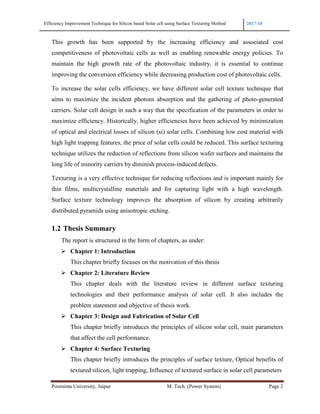
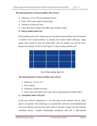
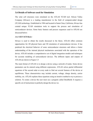
The dissertation presents a technique for improving the efficiency of silicon-based solar cells through surface texturing methods, which enhance light absorption. The research reviews prior studies to identify gaps, simulates solar cell performance using Silvaco Atlas, and finds that texturing significantly reduces reflection and increases internal reflection for better energy absorption. The work aims to contribute to the development of more efficient photovoltaic technologies, addressing the growing demand for renewable energy alternatives.

![Efficiency Improvement Technique for Silicon based Solar cell using Surface Texturing Method 2017-18
Poornima University, Jaipur M. Tech. (Power System) Page 5
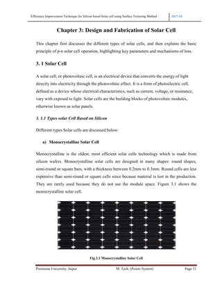
Table 2.1: Issue of Efficiency Improvement Technique for Silicon based Solar cell using Surface
Texturing Method
S. No Name of Issues
Number of Paper Reviewed
Total paper
Conference Journal
1 Design and Modeling of Solar
Cell 3 4 7
2 Efficiency and Parametric
Variation on Solar Cells 4 9 13
3 Manufacturing Cost Consumption
and Time Saving 1 4 5
2.1.1 Issue 1: Design and Modeling of Solar Cell
[Xiaorang Tian et-al, 2015] studied morphological pyramids and etching quantities during
texturing formation processes. They found that the pyramid had a linear association with
the amount of shaping at the transition points of the (100) to (111) planes. 200µm thickness
of phosphor-doped n-type Si wafers 5inch with 3Ωcm resistivity was used. Initially, a
solution of NaOH was used to remove the saw blades. The platelets are formed using
alkaline solutions of chemical etching and after that analyzed for pyramidal morphology
and the quantities of samples forming at certain significant points in the texturing process,
by scanning electron microscopy (SEM), light microscopy and an electronic scale. Cleaning
the wafer by using RCA cleaning procedures, followed by the deposition of a-Si:H film,
using a parallel plate RF PECVD reactor operating at a frequency (13.56MHz). They
observed a surface passivation inherent to a-Si:H layers with a thickness of about 40nm,
which were deposited using precursors SiH4 and H2 to symmetrically form a-Si:H/c-Si/a-
Si:H MCLT test structure. Solar cells were made using texture wafer of different sizes of
pyramids. They indicate that the size of the pyramids can be controlled by observing and
varying the amount of shaping at the point of transition. Mean dimensions of pyramidal
were 0.5µm to 12µm. When the size of the pyramid was less than 1µm or greater than
12µm, it affects the light reflection, life expectancy and productivity of heterojunction](https://image.slidesharecdn.com/divyashikha-210715045210/85/Efficiency-Improvement-Technique-for-silicon-based-Solar-cell-using-Surface-texturing-Method-18-320.jpg)
![Efficiency Improvement Technique for Silicon based Solar cell using Surface Texturing Method 2017-18
Poornima University, Jaipur M. Tech. (Power System) Page 6
silicon solar cells. The result showed that the impact directly affects the density of photo
generated charge carriers, reversing the tendency of JSC to increase first and decrease
considerably increasing the size of the pyramid [2].
[Matthew B.Edwards et-al, 1997] had demonstrated the property of anisotropic
structuring on the existence and cell performance of the structures of the hetero-junction
layer of i-Si layer. Isotropic etching processes are included for remove metal contamination
preceding to deposition of Si and annealing of deposited i-layer. They showed the
preparation of embossed surfaces with sodium hydroxide before the deposition of an
amorphous silica inner layer. N-type wafer having the (100) orientation was subjected to a
random pyramid form using a 2 percent NaOH solution with 2-propanol, put in as wetting
agent NaOH, were submitted to RCA2 own, engraving, or together. The RCA2 solution
consists of 1:6:1 HCL: H2O:H2O2, the mixture was heated to near 80°C for 5 minutes. CP
etching consisted of random pyramidal shaping using a 2% NaOH solution with 2 percent
propanol mixed as a wetting agent. The CP columns are composed of 300mL of HNO3,
10mL of CH3COOH and 40mL of HF and range from 0 to 60s. The surface of the wafer
was cleaned in H2O2/ H2SO4, followed by a decrease in HF. The samples were instantly
transferred to the deposition system and Si deposited on both sides of the plate to a
thickness of 10nm. The deposition was conceded by a plasma enhanced chemical vapour
deposition (PECVD) method and a ratio of dissolved hydrogen to silane. The application of
the layer I is annealed at ~ 300 ° C. in the air for a time ranging from 0 to 70 minutes. Then,
again the wafer was transferred into the PECVD system for the deposition of a layer of a-
Si, deposited by a p-type, face and n-type dosed a-Si back layer. Finally, the contacts were
added, consisting of Al/Ni grids and transparent conductive oxide at the front and an
aluminum back cover. They suggested that a chemical polishing engraving of NaOH
texturing or at low temperatures, which were annealed after texturing with the accurate
deposition parameters, can achieved effective wafer existence which exhibits excellent
passivation of the area. They also suggest that correct wafer surface preparation can lead to
excellent solar cell performance [3].](https://image.slidesharecdn.com/divyashikha-210715045210/85/Efficiency-Improvement-Technique-for-silicon-based-Solar-cell-using-Surface-texturing-Method-19-320.jpg)
![Efficiency Improvement Technique for Silicon based Solar cell using Surface Texturing Method 2017-18
Poornima University, Jaipur M. Tech. (Power System) Page 7
[Su Zhou et al, 2013] proposed acid texturing multi crystalline silicon slices, to improve
trapping incident light and enhance the efficiency of solar cells. Acid texturizing solution
had been considered to reduce grain boundaries and imperfections that can occur in the
texturizing method. For texturing a mc-Si p type, as a base 156 x156mm2
wafer thickness of
200µm using with a resistivity 1 to 3Ω-cm. This process takes place on RENA through the
texture. Firstly, the wafer was formed using acid mixtures including various ratios of HF,
H2O and HNO3 to optimize the solution that was formed. Wafer of different depths of
etching were then obtained by controlling the formation time. Then, the emitter was
dissipated by phosphorus with a POC13 at 835° C in an open furnace. After removing glass
phosphor film, Si3N4 films and the edges deposited by PECVD in a conservative plasma
reactor operating at 13.56MHz, by a mixture of ammonia and SiH4 and the temperature
was put at 450°C. Finally, the diffuse wafer of mc-Si was carried out using the paste of A1
and Ar standard protective metallization, by baking in a furnace at a temperature of 930°C.
The reflective surface was passivated at 300-1200nm range and surface morphologies of the
textured samples were measured using spectrophotometer and SEM. Weighted reflection
(Rw) was calculated by integrating the AM1.5 reflection losses at 300-1200nm. Finally,
they concluded that the solar cells efficiency was improved by optimizing the
multicrystalline silicon texturing process [14].
[In-Ji Lee, et al., 2013] proposed a pyramidal texture surface device for solar cells, which
had been filled with silicon nanowires. P-type silicon wafer with a resistivity of 1 to 3Ωcm
and the thickness of 200µm was etched using 2% by weight a solution of KOH, to generate
square pyramids dispersed randomly on the surface of silicon. Pyramid-shaped silicon
wafers were immersed in a mixed solution of AgNO3 (0.068g), deionized water (160ml)
and HF (46ml) for 30s, in order to place nanoparticle Ag masks on the silicon texture of the
pyramid. Then, the pyramid-shaped silicon wafer masks Ag etched nanoparticles with a
solution of FeNO3 (8.16 g), HF(46ml) and deionized water (160ml) for 0, 1, 2, 3, 4, 5, 7, 10
and 15 min, electro-less etching, to produce silicon nanowires on the wafer surface.
Photovoltaic efficiency was evaluated by a solar simulator under the spectrum of solar light
(AM) 1.5. Finally, they came to the conclusion that n-type silicon photovoltaic cell with
nano-silicon coating on the silicon texture pyramid is increased by 10% in PCE compared](https://image.slidesharecdn.com/divyashikha-210715045210/85/Efficiency-Improvement-Technique-for-silicon-based-Solar-cell-using-Surface-texturing-Method-20-320.jpg)
![Efficiency Improvement Technique for Silicon based Solar cell using Surface Texturing Method 2017-18
Poornima University, Jaipur M. Tech. (Power System) Page 8
to a conventional p-type silicon photo-voltaic cell that skipped anti-reflective coating
process.[15]
[K. A. Kavadias, et al, 2013] provided nanocrystalline surface textured with
nanocrystalline columnar structures of 50 to 100nm diameters and 500nm depth, formed by
RIE in multi hollow cathode system. The light that shines on the etched silicon surface RIE
was reflected in both directions between the spikes so that most of them never came back.
The release of the radio frequency from the hollow cathode allowed the amplitude density
of the plasma to be improved relative to the standard parallel RF scattering parameters. The
process of plasma etched had been developed using O2/SF6 mixture to produce a random
silicon textured surface that appears black to the bare eye. The result of texturing was
obtained while using the RF power of 20W of a cathode reactor with their multi hollow
cathode glow. The frequency of RF was 13.56MHz. The partial pressure coefficient of
O2/SF6 was 2.5 and the etching pressure was 50mTorr for the plasma glowing conditions.
The texturing time is 20 minutes. After textured etching using a plasma system with multi
hollow cathodes, the textured surface resembles a black surface. They had effectively
achieved 11.7% efficiency of textured crystalline silicon solar cell using low-cost spin-on
coating doping [16].
[Qiang Wang, et al, 2017] proposed work in which a crystalline silicon quasi-single-cell
solar cell with a combination of mc-Si grains and sc-MCCE nano-texture process. Initially,
all QSC-Si wafers of p-type with resistivity 1-3Ωcm were treated with an etching of
hydrofluoric acid/nitric acid from the texture of the surface. Then the QSC-Si pre-textured
wafers were applied to the MCCE. Then micron-textured wafers were put down with Ag
nanoparticles and etched with a solution of HF/H2O2/H2O, to form the surface of some
nano-pores. The wafers were etched in HF/HNO3 solution to render the nano-pores in the
final nano-texture which was immediately immersed in a 69% HNO3 solution to remove the
remaining Ag nanoparticles. Finally, all QSC-Si nano-texture wafers were accumulated into
cells using a conventional method involving diffusion of phosphorus removal from the back
edge and p-n junction, chemical evaporation delayed plasma SiNx anti reflection layer and
metallization front and back contacts. The efficiency of the nano-textured cells increases
from 18.4 to 18.9%, due to the different qualities of the wafers from the bottom to the top](https://image.slidesharecdn.com/divyashikha-210715045210/85/Efficiency-Improvement-Technique-for-silicon-based-Solar-cell-using-Surface-texturing-Method-21-320.jpg)
![Efficiency Improvement Technique for Silicon based Solar cell using Surface Texturing Method 2017-18
Poornima University, Jaipur M. Tech. (Power System) Page 9
of a Qsc-Si, and the color difference in the Qsc-Si cells was depressed. Parallel model used
subcell, which explains the characteristics of the QSC-Si cell, which is mainly limited by
the worst subcell. The results show that the efficiency of QSC-Si solar cells is 18 % more
than that of mc-Si solar cells [24].
[Fenqin Hu, et al., 2017] had been developed alkaline etching two-step process for
forming a flat surface on the wafer, which can be rapidly and almost isotropically etched by
immersion in a hydroxide solution. This etching process leads to the formation of a uniform
nanostructure. In order to use the basic process of forming a combination of isotropic
production process and MCCE mc-Si solar cells, the characteristics of these photovoltaic
devices have been studied in detail. There is a p-type mc-Si wafer with a resistivity of 1 to 3
Ωcm, a size of 156 × 156 mm 2 and a thickness of 180 mm. Any raw mc-Si wafers before
etching in the same production batch was immersed in a 4% HF solution for 5 minutes to
remove the native oxides and then rinsed in deionized water. In step 1, the two types of mc-
Si platelets are Damage Elimination Engraving (DRE). The etching solution in an HNO3/
HF wafers mixture labeled H-DRE, and the first etching in a NaOH solution, then etched in
the slice of a NaOH/NaCl solution is identified as the N- DRE. In step 2, the same MCCE
process is performed on both layers of H-ERD and N-ERD. In this process, first, with the
coating layer of Ag nanoparticles, then etching in a solution of mixing HF/H2O/ H2O to
form a nano-porous surface. After the NaOH/H2O etching solution in the nanopores of the
pretend pyramid, and finally all the platelets were immersed in 69% HNO3 to remove the
remaining Ag nanoparticle. The manufacturing process, the wafer is designated as H-DRE
mc-Si, H-DRE Bmc-Si, and N-DRE Bmc-Si. In step 3, the plates are assembled in the cells
(20 samples each) and the formation of a phosphor diffusion n + emitter, the removal of the
edge and back p+
junctions, chemical vapour phase antireflection activated by SiNx plasma
and the passivation layer having a thickness of 80 nm, and screen printing, to form the
sample Ag and Al+ contact in the back surface. The etching process results in the formation
of a homogenous nanostructure improve repeatability and performance of the cell, while
increasing the short circuit current and the open circuit voltage. [25]](https://image.slidesharecdn.com/divyashikha-210715045210/85/Efficiency-Improvement-Technique-for-silicon-based-Solar-cell-using-Surface-texturing-Method-22-320.jpg)
![Efficiency Improvement Technique for Silicon based Solar cell using Surface Texturing Method 2017-18
Poornima University, Jaipur M. Tech. (Power System) Page 10
[Rahul Dewan, et al., 2011] investigated the propagation of optical waves in
microcrystalline thin-film silicon solar cells with pyramidal surface structures and
compared to the theoretical limitations of light capture. The effect of texture duration,
texture height and microcrystalline silicon diode thickness on short-circuit current and
quantum efficiency was also studied. The short-circuit current was maximized for
pyramidal periods of 700 to 1200nm and a height of 400 to 500nm. A comparison of the
simulated quantum efficiency and the short-circuit current with the theoretical limits of
light capture shows that as the thickness of the solar cell increases, the structure reaches its
limit. The comparison of simulated quantum efficiency and short-circuit currents with the
theoretical limit of light capture showed that the structures reached the limits with
increasing solar cell thickness. In order to improve the absorption in the silicon layer i, the
parasitic losses in the solar cell must be minimized. Optically improved short-circuit current
the thinner solar cells have the highest relative gain. For a solar cell with an absorber
thickness of 500nm, the simulated solar cell has a gain of 106%. At an absorber thickness
of 3500nm, the relative gain is reduced to 27%. The main mechanism of cell loss is
reflection, not loss of absorption. As solar cells become thinner, effective light harvesting
techniques can guide the absorption of light into the cell to become more important.
2.1.2 Issue 2: Efficiency and Parametric Variation on Solar Cells
[G.Kumaravelu et al., 2002] had developed a reactive ion etching process for surface
texturing. The monocrystalline silicon had a thickness of 500µm, was cut into a p-type of
20x20mm and a resistivity of 1Ωcm was used as a substrate. Photolithography was
performed using a conventional mercury beam alignment mask characterized by broadband
illumination with a dominant wavelength between 313 and 600nm to define the pattern. In
all experiments, the exposure time was 35seconds. In the lithographic substrate, a
chromium mask on the glass was used. A commercially available g-line photoresist is used
to define the template. All samples were developed with Shipley MF320 developer in
deionized water at a 3:1 dilution for 10seconds.The etching technique is used to create hole-
type structures and the pickup technique to create column type models. NiCr 40nm was
evaporated on the substrate.For the surface texture, three structures were compared: the
structure of the column. It can be seen that on three types of textured surfaces, the reflection
decreases at a wavelength of 250 to 2500nanometers. In particular, at a wavelength of 250](https://image.slidesharecdn.com/divyashikha-210715045210/85/Efficiency-Improvement-Technique-for-silicon-based-Solar-cell-using-Surface-texturing-Method-23-320.jpg)
![Efficiency Improvement Technique for Silicon based Solar cell using Surface Texturing Method 2017-18
Poornima University, Jaipur M. Tech. (Power System) Page 11
nm to 1000nm including the visible region, as expected, the reflection greatly decreases
relative to the polished silicon surface. Conical surface of the reflective structure at a
wavelength less than 400nm at 1000nm is 0.4%, with a minimum of 0.29% at 1000nm,
which is much smaller than the reflection factor obtained in the opening. The untreated
silicon wafer had a reflectance of about 40% at a wavelength of 400nm to 1000nm and at
least 32% at 1000nm. By way of comparison, the reflection of the pore structure was about
8.8% at a wavelength of 400nm to 1000nm, and the minimum value at 1000nm was 4.8%.
The pore structure has a higher reflectance than the column structure at a wavelength of 400
nm to 1000nm. At wavelengths greater than 1000nm, it shows about 8% less reflection than
the column structure, but this may be due to the support layer used in the measurement. The
reflectance of the surface without the etched surface is less than 1.4% at a wavelength of
400 nm to 1000 nm and a minimum of 0.8% at 1000nm.column, pore and black silicon of
Different texturing structures were examined and compared in wavelength and it was found
that the reflection of the textured columnar structures was less than 0.4% at wavelengths of
500nm at 1000nm and shows a minimum of 0.29% 1000nm, while the reflection of black
silicon was about 1% and the hole structure is about 6.8% in the same wavelength range
[1].
[E. Manea, et al., 2007] had proposed an experimental study on increasing the efficiency
of silicon solar cells using texture techniques on the front surface. The texturing processes
of the surface of the high efficiency solar cells were used monocrystalline silicon wafers
doping with boron having resistivity 1-2Ωcm and thickness 380um. They were considered
three types of surface texture these are regular pyramids structure, honeycomb structure and
electrochemical porosification of the silica. First two textures are prepared by the processes
of the integrated circuit technology planar i) increase the surface of the silicon wafer the
with silicon dioxide layer of 800nm thickness as mask of etching (ii) the process of
photolithography on the basis of positive photo resist, which are carried out the windows
scratched in silicon dioxide. In the case of a honeycomb, the windows are 4µm,
respectively 6µm in diameter and were also spaced above an equilateral triangle with 20µm
side on entire surface of silicon wafer. Silicon was isotropically etched with two types of
acid solution HNO3:NH4F:HF:H2O-(280:6:3:140) and CH3COOH:HNO3:HF-(10:25:1). The
shaping deepness was 7µm and 5µm respectively. For the solution of HNO3:](https://image.slidesharecdn.com/divyashikha-210715045210/85/Efficiency-Improvement-Technique-for-silicon-based-Solar-cell-using-Surface-texturing-Method-24-320.jpg)
![Efficiency Improvement Technique for Silicon based Solar cell using Surface Texturing Method 2017-18
Poornima University, Jaipur M. Tech. (Power System) Page 12
NH4F:HF:H20-(280:6:3:140) during etching was 10 times smaller compared to
CH3COOH:HNO3: HF- (10:1:25) uniform on the entire surface of silicon wafers and good
etching time management. The application of texture processes with small masks leads to
reflections of less than 10%. Photolithography was used to produce samples through the
SO2 layer first developed on silicon wafers. The holes were equally spread all over the
surface and the find the distance between the centers of holes was defined as 20µm. The
Semispherical walls were placed in holes with isotropic etching until the walls of the
adjacent walls meet. For the pyramidal walls formation a photolithographic technique and
etching were used in a 40% KOH solution. The texture of an antireflection layer obtained
by oxidation of silicon leads to a reflection reduction of less than 5%. The antireflection
technique applied to the solar cells leads to a significant increase in the trapping of light in
the structure, which make it possible to achieve conversion efficiency greater than 20% [7].
[Hayoung Park, et al., 2009] used mixture of aqueous acidic acid for the saw-damage
etching process. The etching of silicon is isotropic in nature. The aim of the author is to
improve the final texture of the surface by using an acid etching of the saws to produce
small pyramids of regular shape. SEM and spectrophotometer was used to estimate the
surface of textured. Mono-crystalline silicon wafers with resistivity’s 6–12Ωcm and
thickness of 270m. Wafers surfaces were first cleaned to remove all organic and metallic
impurities. For this cleaning process, sulphuric acid mixed with a solution of hydrogen
peroxide (SPM) and hydrochloric acid mixed with a solution of hydrogen peroxide (HPM)
was used on the basis of a standard RCA cleaning. After soaking thoroughly with de-
ionized water (DIW) between every cleaning stage, the wafers were soaked in a buffed
oxide etching (BOE) to remove the natural oxide layer. In comparison, the wafers were
prepared with three different surface morphologies. Section 1 was not saw-damage-etched
wafer and section 2 was saw-damage etched with KOH solution. At last Sample 3 wafers
were saw damage etched with an aqueous acid mixture. All wafers were then
anisotropically formed etched using solution mixture of KOH and IPA. It showed that acid
etching saw damage had the potential to get better cell efficiency. Compared to the alkali
saw-damage-etched solar cell, JSC for acidic saw-damage-etched solar cell increases almost
10% indicating effective capture of photons due to the textured surface [8].](https://image.slidesharecdn.com/divyashikha-210715045210/85/Efficiency-Improvement-Technique-for-silicon-based-Solar-cell-using-Surface-texturing-Method-25-320.jpg)
![Efficiency Improvement Technique for Silicon based Solar cell using Surface Texturing Method 2017-18
Poornima University, Jaipur M. Tech. (Power System) Page 13
[yuang-tung cheng, et al, 2011] proposed an acid texturizing method for multicrystalline
silicon solar cells (mc-Si) to improve their efficiency. The acidic texture is cheap, fast, very
simple, inexpensive and suitable for mass production. P-type Mc-Si wafer was used with
resistivity of 0.1-0.5Ωcm and a thickness of 300µm with 125mm×125mm. The isotropic
acid test for the mc-Si wafers was carried out with a mixture solution HNO3 and HF.
surface texturing and removal of the saw damage layer can be accomplished in one step for
an acidic etching solution. The substrate of the mc-Si solar cell was initially etched with the
HNO3, HF and H2O acid mixture in a 1:2.5:2.5mixture for 20s, 15s, and 25s. The etching
time for the four different set was taken as 120s, 60s, 30s and 25s. All etching was
performed at room temperature. All the samples of textured were measured with a
spectrophotometer and the surface of the samples was examined under a SEM. In order to
compute the PV effect, the I-V curves were represented on a curve tracer. The IQE curve
with an acidic solution (HNO3:HF:H2O =1:15:2.5) is higher than that of the alkaline texture
and non-etching on mc-Si [11].
[Ali Assi et al., 2012] presented the fabrication, characterization, and analysis of mc-Si
solar cells. Authors used an acidic texture method that increases parasitic resistance losses,
provides a grain boundary defect, and degrades electrical characteristics. By varying the
composition of the solution of texture, the defective etching was minimized, but leads to a
polished texture and thus lowers the absorption of incident. In order to improve the incident
light absorption isotropic texture was extensively used with nitric acid (HNO3),
hydrofluoric acid (HF) and demineralized water (DI H2O). The diffusion of phosphorus
temperature, phosphorus concentration, refractive index (RI) of anti reflection coating
(ARC), coating thickness (CT), and the sintering rate of metal electrodes were studied. A
batch of 156mm2
was produced with 16.54% average cell efficiency, which was 0.42%
absolute and the shunt resistance (Rsh) was increased twice compared to the standard
method. They can be analyzed and compared to surface morphology of open circuit voltage
(Voc), short-circuit current (Isc), fill factor (FF), efficiency the cell (η) reflection factor
(RF) [12].
[Yuxin Xia, et-al, 2013] proposed pyramid-shaped PSCs with trapping of light in the entire
360◦ directions as well as complete space utilization when assembled into device. The](https://image.slidesharecdn.com/divyashikha-210715045210/85/Efficiency-Improvement-Technique-for-silicon-based-Solar-cell-using-Surface-texturing-Method-26-320.jpg)
![Efficiency Improvement Technique for Silicon based Solar cell using Surface Texturing Method 2017-18
Poornima University, Jaipur M. Tech. (Power System) Page 14
advantage of a pyramidal PSC was that it can fully utilize the limited space. The pyramidal
device consists of four independent triangular solar cells with a fixed area of 1cm2
for each
of them. These triangular solar cells are placed on a certain pyramid-shaped support which
serves as four lateral sides of the pyramid so that the lateral surface of the pyramidal device
was a total of 4cm2
. Eight copper contact probes used to mount on the support, two for
each cell which could establish close contact with the electrodes of the solar cells. Probes
can be connected with the cells in series, parallel and in series parallel to obtain an
appropriate Voc and a suitable JSC. The absorption of light depended on the angle of two
opposite sides of the pyramids (β). The absorption throughout the entire visible range
became stronger when β decreases from 180° to 30°. Decrease in β due to the irradiated
light on the active layer per unit area may be weaker and thus the light can be absorbed
more efficiently. When β decreases, the lighting will probably be reflected more times,
which means more light absorption time in the device and it also helped the light trapping.
Thus, when β decreases, the effect of lighting of the light is more efficient which leads to an
increase in the collection of photons and Jsc [13].
[Dimitre Z., et-al, 2013] proposed random upright pyramids microtexture on
nanostructured silicon surfaces, obtained by electroless processing in Na2S2O8 solution,
followed by etching in H2O2/HF/H2O. In the KOH-IPA solution at 80°C for 45 minutes was
performed texturization with micron sized random pyramids. Textured wafers were cleaned
in a mixture of H2O2:HCl:H2O at 80°C for 10minutes and then wafer surfaces H-terminated
in diluted HF. Random nano pyramid texture was produced by a two-step method
consisting of electroless treatment in an acid aqueous solution of AgNO3 (pH <3) and
Na2S2O8 for 6minutes followed by etching in aqueous solution of H2O2 and HF and for
2min. Both treatments were performing at room temperature on a wafer of pseudo-square
with length 125cmx125cm. The details of the preparation of the electroless solution were
described in the. The normal sheet resistance after diffusion of phosphorus oxychloride
(POC13) and the removal of phosphorus-silicate glass (PSG) in dilute HF was calculated at
about 80Ω/square. After PECVD deposition of antireflection and SiNx passivation layer on
the front surface of the wafer, the contact with the silver pattern and the aluminum surface
of the back surface were formed by screen printing and co-firing in an infrared belt furnace.
The overall reflectance of texturized wafers and solar cells was measured with a Hitachi U-](https://image.slidesharecdn.com/divyashikha-210715045210/85/Efficiency-Improvement-Technique-for-silicon-based-Solar-cell-using-Surface-texturing-Method-27-320.jpg)
![Efficiency Improvement Technique for Silicon based Solar cell using Surface Texturing Method 2017-18
Poornima University, Jaipur M. Tech. (Power System) Page 15
3010 spectrophotometer equipped with an integrating sphere in the wavelength range of
300-900nm. The wafer surface morphology was examined by a SEM technique. For SEM
measurements were drawn square pieces of 20mmx20mm, using laser cutting. Finishing
performance of solar cells was analyzed by reflection, quantum efficiency and I-V
measurements. Determination of the current-voltage (I-V) parameters of the solar cell was
carried out at 25°C under AM1.5G solar spectrum using a Wacom solar simulator an output
power of 1000 W/m2
. Nanoporous structure with relatively shallow pore depth and reduced
contact emitter leads to improved blue response and increased Voc and JSC in two-
dimensional textured cells [17].
[Ayman Ahmed, et-al, 2015] proposed surface texturing techniques with an alkaline
solution for monocrystalline Si (c-Si) solar cells were usually accepted to enhance cell
performance. Multicrystalline cells (mc-Si) were complicated to form by alkaline etching
due to the grains of the substrate are randomly oriented. They considered the HF/HNO3
/H2O acid solution to texturize the mc-Si cells. The isotropic textureing of the mc-Si wafer
was performed using a mixture of HNO3 and HF. For an acidic removal of saw damage,
etching solution and surface shaping can be accomplished in one step. The rate of etching
was about 5m/min. A sequence of experiments based on acid etching was performed by
various processes. In the first part of the mc-Si solar cell prototype experiment, the
substrate was etched with the sequence of an acid solution of H2O, HF and HNO3 and in a
mixing ratio of 2.5:2.5:1 at 25s, 15s and 20s. When optimizing the shape, the HF ratios are
changed in three different recipes of 5, 15 and 30. The duration of the etching of the four
different sets is taken as 120s, 60s, 30s and 25s. Every etching was performed at room
temperature. Conversion efficiency of the mc-Si solar cells, textured with the HNO3/HF
/H2O=1:30:2.5 solution had comparatively high values. The optimal ratio of HNO3:HF:H2O
= 1:30:2.5 bind with etching time of 60s and a reduction of 41.9% compared to the R value
can increase 111.8 % of the conversion efficiency (η) of the solar cells. The acid texturing
approach is a tool for achieving high efficiency in mass production, using a comparatively
low cost mc-Si as an initial material with the appropriate optimization of the fabrication
stages [18].](https://image.slidesharecdn.com/divyashikha-210715045210/85/Efficiency-Improvement-Technique-for-silicon-based-Solar-cell-using-Surface-texturing-Method-28-320.jpg)
![Efficiency Improvement Technique for Silicon based Solar cell using Surface Texturing Method 2017-18
Poornima University, Jaipur M. Tech. (Power System) Page 16
[Min Young Kim, et-al, 2015] proposed the effect of surface texture on the efficiency of c-
Si solar cells. To examine the effect of the texture, the solar cells were produced with
different surfaces textured using conventional anisotropic etching of a combination of
isopropyl alcohol and KOH, RIE and Ag-catalyzed etching. They used p-type
monocrystalline Si wafer of a thickness of about 200µm and a resistivity of about 1.5 Ω-cm.
The abrasive wafers were etched using KOH to eliminate surface damage caused by the
saw wires. After elimination of the damage had many different texturing techniques,
including conventional anisotropic etching (CAE) with a combination of KOH, isopropyl
alcohol (IRA), Ag-catalyzed etching (ACE) and reactive ion etching (RIE). They also
realized a macro-micro textured mixing method in two steps. They used the following
procedure: The first etching was done using CAE. The textured Si plate was then etched
again using RIE or ACE. After the surface treatment, the m-Si solar cells were prepared
with a 60Ω/square n-type emitter by performing a conventional diffusion of POCL3. The
Phosphosilicate glass (PSG) glass layers on wafer surfaces were removed by immersing
them in a solution with a buffered oxide etch (BOE) for one minute. To deposit a layer of
silicon nitride (SiNx) with a thickness of about 76nm using PECVD as a passivation layer
and an antireflection layer on the front surface at 400°C. The refractive index of the SiNx
film was maintained at 1.95. The front and rear metallizations were carried away by a
screen printing technique with a standard Ag paste for the front surface and an Al paste for
the rear surface. The metal contacts were produced by rapid thermal process (RTP), which
has a maximum temperature of about 620°C. Surface morphologies of Si were analyzed
using SEM with working voltage of 10kV. Reflections of textured Si wafers were measured
using spectrophotometer in the visible range of wavelengths of 400-1000nm. The Si wafers
resistances were measured using a 4-point probe. Current voltage characteristics were
measured using a McScience Lab 50 solar simulator with AM1.5G illumination at an output
power of 100mW/cm2
. The reflection of the textured surfaces ranges from 9.11% to 1.47%
at wavelengths between 400 and 1000nm. In the case of CAE samples, the surface
reflection was 9.11%. The RIE and ACE samples respectively had a reflection of 5.41%
and 5.44% respectively. In the case of two-step etching, the surface reflections were 2.65%
(CAE + RIE) and 1.47% (CAE + ACE). The reflection of the textured Si surface at two
stages was lower, especially at shorter wavelengths. Among the five different solar cell](https://image.slidesharecdn.com/divyashikha-210715045210/85/Efficiency-Improvement-Technique-for-silicon-based-Solar-cell-using-Surface-texturing-Method-29-320.jpg)
![Efficiency Improvement Technique for Silicon based Solar cell using Surface Texturing Method 2017-18
Poornima University, Jaipur M. Tech. (Power System) Page 17
structures, the solar cell with a two-step textured CAE / RIE combined structure showed the
highest efficiency at 17.78%. It also had a JSC of 37.46mA /cm2
, a Voc of 0.614 V and a FF
of 77.34% [19].
[Ngwe Zin1, et-al, 2016] proposed pyramid rounding textured to improve the conservation
of light. Samples with round and round flat pyramidal form were used. In rounding form a
burning time of 60seconds was accepted for this evaluation. The cells consist of high-
strength FZ plates <100>. The cells with flat and rounded pyramidal structures had a final
thickness of 230µm and 170µm. The current-voltage, measured in the sun, using an internal
solar simulator. Double-sided texture including rounded rare texture, while keep a relatively
low surface recombination. Increasing the rounding time when etching makes the pyramids
with a smaller and smoother texture; resulting in enhanced passivation of the surface. The
rounded textured pyramids reduce Jo up to 65% and Jo fully textured pyramids. Ray tracing
proposed that optimum trapping of light would came from the partially rounded rear
pyramids. Jsc of rounded cells textured compared to that planar rear cell was increased by
0.25mA/cm2
[20].
[A. Hamel, 2016] presented detailed study of light transmission through the textured
surfaces of pyramids, and analyzes the optimal texture of the surface to provide the best
trapping of light to solar cells at the total internal reflection occurring in the medium with a
high index and the nominal critical angle value. The author also analyzed the impact of the
opening between the heads of the two pyramids closest to the textured surface of the solar
cells and its application on photovoltaic parameters such as quantum efficiency. The
material may have five or more consecutive absorptions of incident rays instead of three, as
they change the direction of the reflected beam by changing the angle between the two
adjacent pyramids, the angle of inclination, the incidence angle, the opening between the
heads of the two nearest pyramids and their height. Thus, the angle between the two
adjacent pyramids varies between 20° and 12° and the angle of the incidence was between
80° and 84°. For these values of the angle between the two adjacent pyramids and the angle
of inclination, the opening between the heads of the two nearest pyramids varies
respectively from 3.53 to 2.10µm in a pyramid having a height of 10µm. This led to a
significant increase in quantum efficiency, hence photovoltaic efficiency. The variation of](https://image.slidesharecdn.com/divyashikha-210715045210/85/Efficiency-Improvement-Technique-for-silicon-based-Solar-cell-using-Surface-texturing-Method-30-320.jpg)
![Efficiency Improvement Technique for Silicon based Solar cell using Surface Texturing Method 2017-18
Poornima University, Jaipur M. Tech. (Power System) Page 18
the absorption coefficient as a function of the reflectance shows different curves
representing the internal quantum efficiency as a function of the reflection coefficient of the
textured photovoltaic cell with cell thickness d = 100µm and L diffusion length =100m.
This difference was compared to the ideal case, in the case of a plane normal to that of the
texture plane was a link for different values of the internal quantum efficiency, which
showed that they were closer to the ideal values if they wanted to take advantage of ray
incidence five times, then the fourth, then three, twice as much as that. The result obtained a
good result, especially for the processed surface of the plane, where the reflection
coefficient r was close to zero and thus the internal quantum efficiency increased almost to
the ideal value [21].
[Sanjay K. Sardana, et-al, 2016] Investigated the effect of SiO2 spacer layer thickness
between the textured silicon surface and silver nanoparticles (Ag NPs) on solar cell solar
cells having a thickness of 200 ± 10 µm without antireflection layer were used. POCL3
diffusion was used for the fabrication of cell. The front and rear contacts were prepared
from Ag and Ag/Al metals, respectively, using a screen printing process. Areas of Small
cells 2.5 to 4 cm2
were used for experimental purposes after cutting large size cells of
standard size. The different thicknesses of SiO2 100, 70, 50, 40 and 300nm layers were
deposited on these cells by RF magnetron sputtering. The refractive indices of the
powdered SiO2 films were evaluated using an ellipsometry of 1.45. SiO2 was applied at an
operating pressure of 4x10⁻²
mbar in an argon gas atmosphere at a flow rate of 20sccm with
an RF power of 200W. Thin solid films having a thickness of 10nm, was also deposited on
the solar cell with and without the SiO2 layer using the same RF sputtering system, but with
a power of 20W. Finally the cells were annealed at 300°C in nitrogen gas environment for
1h to convert Ag ultra-thin film into NPs. A SEM was used to study the surface
morphology of Ag NPs. spectra quantum efficiency measurement system, equipped with a
solution integration sphere RERA, The Netherlands, was used to record the spectra of
external quantum efficiency (EQE) and total reflection. These measurements were
performed under AM1.5G lighting conditions with an incident light power of 100mW/cm2
.
The EQE and Total Reflection spectra were used to calculate the internal quantum
efficiency (IQE) of the cells. AAA class solar simulator by Oriel Newport Corporation,
USA, and the Keithley 2440 output meter was used to measure current density and voltage](https://image.slidesharecdn.com/divyashikha-210715045210/85/Efficiency-Improvement-Technique-for-silicon-based-Solar-cell-using-Surface-texturing-Method-31-320.jpg)
![Efficiency Improvement Technique for Silicon based Solar cell using Surface Texturing Method 2017-18
Poornima University, Jaipur M. Tech. (Power System) Page 19
(J-V) by illuminating the front of the cell. In order to calibrate the xenon light source, a
certified solar cell from NREL, USA had been certified. The EQE and J-V measurements
were performed on the same cells before and after the deposition of Ag NPs on layers of
SiO2 of different thickness to avoid variations in the electronic properties of the cell. All
these measurements were performed at room temperature. Photovoltaic parameters such as
current density (Jsc), series resistance (Rs), fill factor (FF) and efficiency (η) were affected
due to the cell configuration modified with Ag NP on the layer Optimized SiO2 spacing.
Due to the increased light scattering of NPs Ag in silicon, Jsc increases from 22.23 to
23.81mA/cm2
, increasing efficiency of cell efficiency from 8.7 to 10.0%. They found that
the optimized spacing SiO2 layer was between 30 and 40nm for for enhancing the
photocurrent in the off-resonance (longer) wavelength region and maintenance nearly same
in the SPR region of the Ag NPs. A high thickness of SiO2(≥ 70 nm) has reduced quantum
efficiency clearly demonstrated that to maximize cell efficiency, the spacer dielectric layer
must provide electronic isolation without self-absorption and the optimal coupling
generated close to Ag NPs fields in the silicon base material after the interaction of light
[22].
[Khaldun A. Salman, 2017] had been proposed two texturing methods using porous
silicon (PS) and pyramids to study the improvement of the efficiency of crystalline silicon
solar cells (c-Si). He also showed the representation of c-Si solar cells with different
texturing processes. N-type c-Si substrate orientation (100), 283µm thickness and resistance
0.75Ωcm were used as a substrate for surface texturing using PS and pyramid processes.
Before the texturization process, the c-Si plates were cleaned in H2SO4:H2O2 (2:1) solution.
To perform PS, place the plate in an electrolytic solution (HF: ethanol, 1: 5) with a current
density of 40mA/cm2
and 25min. etching time using a photo-electrochemical cell (PECE)
that was made of teflon and has a circular aperture at the bottom that was sealed by the c-Si
sample. The cell has a two-electrode system connected to the c-Si sample as anode and
platinum (Pt) as the cathode. The morphology of the topography of the surface was
characterized by SEM and AFM, with a high density of nano-pores with high porosity were
produced in the PS layer compared to the lower density nano-pyramids with low porosity
were apparently distributed randomly on the surface of N-type c-Si (100). The high degree
of roughness was confirmed by the higher mean square, which was 330.64 nm for the PS](https://image.slidesharecdn.com/divyashikha-210715045210/85/Efficiency-Improvement-Technique-for-silicon-based-Solar-cell-using-Surface-texturing-Method-32-320.jpg)
![Efficiency Improvement Technique for Silicon based Solar cell using Surface Texturing Method 2017-18
Poornima University, Jaipur M. Tech. (Power System) Page 20
layers compared to 110.30nm and 2.65nm of Si grown and the texturing of the pyramids.
The light characteristic traps in the PS layer was no longer possible because of the increase,
it significantly reduces the reflection of light with a wavelength in the range of 350-1050nm
compared to the texturing of the pyramids and growing Si. Results showed that the high
conversion efficiency of 13.23% for the PS layer compared to 11.36% and 37% efficiency
for solar cell devices with a pyramidal and Si-grown texture, respectively. The PS texture
showed an excellent reduction of the reflection of the incident light with respect to the
pyramidal process, with a good light-trapping of wide wavelength spectrum which could
produce high efficiency solar cells. [23]
2.1.3 Issue 3: Manufacturing Cost Consumption and Time Saving
[D.H. Macdonald, et-al, 2004] proposed three texturizing methods: wet acidic texturing,
masked and maskless Reactive Ion Etching (RIE) for commercial multicrystalline silicon
solar cells, based on the measurement of reflectance. They found that the three texturing
methods significantly reduced reflection losses in solar cells. They also studied as as-cut
wafers that remain in a damaged state after cutting the wafer. An acidic textured wafer was
made with a HF / HNO3 solution. A wetting agent is added to obtain a more even structure.
Approximately 5-10µm of silicon was removed from each surface. Surface damage was
removed, but its initial presence was critical because it acts as a seeding layer for texturing.
The wafers were placed at random, but the deep features with steep walls that offer very
little reflection. The RIE light plates were much smaller than those of the acid textured
sample. The RIEs were very regular and steep, with a distance of 7µm between the
pyramids. The pyramids were about the same as those of the wet acid texture wafer.
Textured RIE slices create an even greater increase in current compared to the predicted
controls, from 28.25 to 30.63mAcm2
. So, finally, they suggested that the reduction of
impact was most noticeable for masked RIE pyramids, attracted by masked RIE, and then
acid texturing. As a result, the relative distinction between strategies was greatly reduced
after antireflection coverage and encapsulation. In addition, they mentioned that the
implementation costs were much less acidic texturing than RIE processes, especially the
masked RIE. [4]](https://image.slidesharecdn.com/divyashikha-210715045210/85/Efficiency-Improvement-Technique-for-silicon-based-Solar-cell-using-Surface-texturing-Method-33-320.jpg)
![Efficiency Improvement Technique for Silicon based Solar cell using Surface Texturing Method 2017-18
Poornima University, Jaipur M. Tech. (Power System) Page 21
[Saifuddin M. lalil, et al.2008] had investigated various models of GaAs solar cells with
different texturizing surfaces to improve the spectral sensitivity of photovoltaics by
reducing light reflection and improving light trapping. Four surface texture models were
used: simple structure, four-sided structure, semisphere structure and V-shaped structure of
photovoltaic device. An <100> orientation of a GaAs buffer was selected with a 10
substrate thickness and a concentration of boron was 1×10¹⁷
cm. The p-n branch was
developed by phosphorus doping implantation with 1x10¹⁷
cm-3
and 5eV energy. The anneal
time 300minutes and the anneal temperature 900°C were constant. By changing four
variables of the surface texture, the solar cell with the single p-n can be simulated. By
plotting the characteristic I-V graph, a single-surface solar cell with a three-patterned
textured surface was compared. For the surface treatment technique of solar cells, the
ATHENA software was used as a method of shaping the surface structure. The lowest
efficiency was 20.95%, derived from the normal structure of the solar cell. The V trench
structure was the optimal textured surface for GaAs solar cells compared to the others and
Jsc was 3.5752mA, Voc was 0.800V and efficiency of 23.07% was obtained. They suggest
that the V-trench structure was the best surface texture that has optimal efficiency and
short-circuit current density for the GaAs solar cell than others [5].
[M. Moreno, et-al, 2010] presented a study of the texture of c-Si plates using SF6/O2
plasma in a reactive ion etching (RIE) system. They also determine the combined effect of
RF plasma power and SF6/O2 ratio. They found that by changing the RF power with an
optimized SF6/O2 ratio, it was possible to produce normal or inverted pyramidal structures
with very low reflection values of only 6%. The c-Si texture was realized in a 13.56MHz
RF projection system. Substrates of the p-Si type (100) were used and the resistance was
between 14 and 22Ωcm. Different texturing processes had been systematically studied and
optimized by changing the SF6/O2 ratio from 2 to 10 combined with a wide range of RF
powers (from 25to150 W). For a reliable texture of c-Si, it was found that the ratio of gas
should fall to 3(SF6/O2=99sccm/33sccm). All processes were performed for 15min at a
fixed pressure of 100mTorr. Before each texturing process, they applied oxygen plasma for
5 minutes. A SEM was used to analyze textured c-Si surfaces. The reflection of the textured
samples in the wavelength range of 300 to 1000nm was measured. They used an atomic
force microscope to analyze the roughness of the surface and the profile of the structures](https://image.slidesharecdn.com/divyashikha-210715045210/85/Efficiency-Improvement-Technique-for-silicon-based-Solar-cell-using-Surface-texturing-Method-34-320.jpg)
![Efficiency Improvement Technique for Silicon based Solar cell using Surface Texturing Method 2017-18
Poornima University, Jaipur M. Tech. (Power System) Page 22
produced on the surface of the c-Si plasma. Finally, Raman measurements were made to
analyze the effect of the plasma process on the surface crystallinity of c-Si. They can
observe the formation of SiOx micro-masks. At 50W, at the same time as the plasma
formation, there was an increase in the structure and a decrease in SiOx micro-masks
thickness, the size of which also decreases due to SF6/O2 plasma etching. It was possible
that at low RF power the texture was controlled by an anisotropic chemical process, more
than an isotropic ion assisted etching process. At 100 and 150W there were no more micro-
masks. These results represented a potential alternative for the production of low cost c-Si
solar cells because the process was completely dry, no DI water, wet chemicals or
photolithography was needed. Pyramid-like normal structures in the c-Si surface resulted in
an average reflection of about 18%, whereas pyramid-reversed structures resulted in
average reflection up to 6% without anti-reflective coating [6].
[Jeehwan Kim, et-al, 2010] proposed surface texturing method to reduce the loss of
surface reflection. The author used a layer of low density SiO2 to allow etching in localized
areas such as the etch mask, forming inverted pyramids. The oxide can be deferred by
plasma enhanced chemical vapour deposition using low deposition temperatures. Density of
PECVD oxide films can be controlled by changing the PECVD deposition conditions, as
deposition temperature, plasma power and gas pressure. The deposition temperature was
one of the strong factors that determine the density of the film. They varied the deposition
temperature to deposit SiO2 with different densities. SiO2 film 25nm thick was deposited on
single crystalline. The thermal oxide was also grown at 800°C with the same comparison
thickness. Silicon substrates with various oxides were dipped in a TMAH solution at 90°C
for 5 minutes. This process can be categorized in four steps; Step 1: Formation of inverted
pyramids, step 2: coalescence of inverted pyramids, step 3: removal of masks and
extinction of inverted pyramids, and Step 4: Formation of upright pyramids. Semi-
dimensional reflection of the samples at each step, measured using an integrating and
monochromatic sphere. About 40% of the impact reduction had to form step 1 which had
partially coated the surface of the inverted pyramid. 14% hemispheric reflectivity was
observed for the sample from step 2, which was as good as the effect obtained by the
classical upright pyramidal patterns [9].](https://image.slidesharecdn.com/divyashikha-210715045210/85/Efficiency-Improvement-Technique-for-silicon-based-Solar-cell-using-Surface-texturing-Method-35-320.jpg)
![Efficiency Improvement Technique for Silicon based Solar cell using Surface Texturing Method 2017-18
Poornima University, Jaipur M. Tech. (Power System) Page 23
[Nirag Kadakia, et-al, 2010] proposed a method based on ion implantation and thermal
annealing to produce silicon surface textures for antireflection purposes. The crystalline Si
surface modification by implantation of hydrogen ions was a well-known phenomenon, but
the surface structures generated by the implantation of H, usually low density packing, and
a small proportional amount, were not effective in the suppression of the light reflection of
Si. A critical step towards increasing the efficiency of sunlight to transform electricity
through photovoltaic action was to minimize the impact of sunlight on the surface of solar
devices. Implantation of ionic hydrogen was useful for surface texturing due to the
exfoliation phenomena of Si crystals. Evolution of surface morphologies with quenching of
n-type crystal temperature Si (100), 10-20Ω cm, implanted with 20 kV H ions at the flow of
8.7x10¹⁶
/cm2
. Samples implanted with H, micron sized blisters appeared on the Si surface,
followed by annealing above 500°C for 75minutes, and many of them even inside the
craters. At 1100°C, a noticeable exfoliation of Si, leading to the formation of micron-sized
hillock-shaped structures, poorly distributed on the surface of the sample implanted with H.
Atomic force microscopy indicates that the height of these structures was near 200nm,
suggests that Si delamination occurs at a depth deeper than the maximum concentration of
H at 270nm below the surface. H implantation samples were implanted with 90kV Ar ions,
designed in the 100nm range at room temperature to a fluence of 5.5 x 10¹⁵
/cm2
. Surface
blisters appear at 400°C and they did not evaporate until the annealing temperature does not
exceed 800°C. At 1100°C quite different surface morphology was characterized by
interconnected structures, such as that the depth of 1µm and 1 to 2µm the width, density and
aspect ratio was much higher than those surface textures generated from a single implant H.
The concentration of Ar peaks implanted around 100nm from the surface, Ar implantation
gives amorphous layer starting from the surface at the 300nm depth, close to the maximum
ionic ion implanted distribution, determined by diffusion analysis Rutherford reaction,
respectively. A-Si layer in the formation of surface textures with high density and high-
aspect-ratio of appearance necessary to effectively suppress the reflection of light. The
effect of the interference becomes more pronounced than the thickness of the a-Si layer
greatly decreased after heat treatment at 900°C. They also found that the diffuse reflection
loss of this sample remained below 5%, only slightly higher than that of the polished virgin
1% Si. By changing the energy and the fluence for the Ar ions, they produced different](https://image.slidesharecdn.com/divyashikha-210715045210/85/Efficiency-Improvement-Technique-for-silicon-based-Solar-cell-using-Surface-texturing-Method-36-320.jpg)
![Efficiency Improvement Technique for Silicon based Solar cell using Surface Texturing Method 2017-18
Poornima University, Jaipur M. Tech. (Power System) Page 24
layers of a-Si with a thickness much smaller or greater than 300nm, but these Ar implants
did not give the desired surface texture. In conclusion, the construction of surface texture
based on co-implantation of H and Ar combined with thermal annealing and oxidation was
suitable for Si antireflection. The lowest reflection obtained with respect to the AM1.5 solar
spectrum is 1% for a wide range of the incident [10].
2.2 Common findings under the issues “Efficiency Improvement
Technique for Silicon based Solar cell using Surface Texturing
Method”
I have reviewed 25 research papers which are related to Efficiency Improvement Technique
for Silicon based Solar cell using Surface Texturing Method. To enhance the efficiency of
solar cell authors proposed difference structure modification, different materials and
techniques. Some common findings that are used by the researchers are listed below along
with their brief introduction:
• CP etching or low temperature anneal after texturing with the correct deposition
parameters, can achieve the effective lifetimes of the wafers greater than 1ms, which
exhibits excellent surface passivation[3].
• Alkaline etching to eliminate saw damage and do not create texture produces high
reflectivity. In fact, for samples with this thickness (about 275 mm) perfectly
polished surface will also lead to a reflection of about 34% [14].
• The optimal ratio of etching acid HF: HNO3:H2O=15:1:2.5 with the etching time of
60seconds and the lowering of 42.7% of the reflection improves 112.4% of the
conversion efficiency of the solar cell developed [11].
• The solution HNO3/HF/DI H2O was used for mc-Si solar cells, which considerably
reduces the reflection factor, but also creates a significant number of dark lines in
the grain boundaries known under grain boundary attack GBT. To reduce GBT, they
studied the use of sulphuric acid (H2SO4), acetic acid (CH3COOH) phosphoric acid
(H3PO4) [12].
• Recipe solution for Group A texturing is HF: HNO3: H2O=1: 2: 1.5, and the depth
of shaping is 3.6µm, and that of group B is HF: HNO3: H2O=1: 4: 2 and 4.1µm. The
parameters of the cell, such as open circuit voltage, short circuit current and](https://image.slidesharecdn.com/divyashikha-210715045210/85/Efficiency-Improvement-Technique-for-silicon-based-Solar-cell-using-Surface-texturing-Method-37-320.jpg)
![Efficiency Improvement Technique for Silicon based Solar cell using Surface Texturing Method 2017-18
Poornima University, Jaipur M. Tech. (Power System) Page 25
efficiency, have been improved. This showed that the ratio HF: HNO3: H2O changes
from 1: 2: 1.5 to 1: 4: 2. It was possible to observe the deep grain boundaries and
openings, which can lead to the shunt [14].
• Production process of silicon nanowire using the Ag nanoparticle mask and
electroless etching, should be a key engineering technique that maximizes the
photovoltaic efficiency of silicon solar cells [15].
• P-type silicon photovoltaic cell with nano-silicon coating on a silicon surface with
textured pyramid increased by 10% at PCE, in comparison with the conventional
photovoltaic cell of p-type silicon, where the coating of anti-reflective process
skipped [15].
• Antireflection textured surface property ARNAB was examined and compared with
silicon samples coated with a wet texture and PECVD. A solar cell was used using
low-cost spin-on coating technology. Solar cell using low-cost spin-on coating
technique has been verified. They have successfully achieved 11.7% efficient large
area (98cm2
) ARNAB textured crystalline silicon solar cell using low-cost spin-on
coating doping [16].
• Na2S2O8 treatment, activated by AgNO3 electroless solution and etching in
HF/H2O2/H2O, gave the nanostructure directly onto the pyramids covered silicon
surface was achieved [17].
• Reflectivity values for acid etching and alkali etching were improved by 39.21%
and 2.21% of the value of non-etching [18].
• Textured surface reflections ranged from 9.11 percent to 1.47 percent wavelengths
between 400 and 1000nm, and cell efficiency ranged from 15.83 percent to 17.78
percent [19].
• Samples with a double-sided texture with rounded rare pyramids have a higher light
capture to sample with a flat back surface. Highly potential rounded pyramids in
silicon solar cells results in efficient solar cell production of 24% of the back-
contact [20].
• Evaporation of Silver (Ag) was used on the front (n-type) side of the sample to
structure a metallisation grid pattern and aluminum (Al) evaporation was used on
the rear (p-type) side to form a reflector contact [23].](https://image.slidesharecdn.com/divyashikha-210715045210/85/Efficiency-Improvement-Technique-for-silicon-based-Solar-cell-using-Surface-texturing-Method-38-320.jpg)
![Efficiency Improvement Technique for Silicon based Solar cell using Surface Texturing Method 2017-18
Poornima University, Jaipur M. Tech. (Power System) Page 26
• QSC-Si solar cells with a mixture of SC- and mc-Si grains showed 18.4% efficiency
to 18.9% using their well established nanotexture process and showed that QSC-Si
can be competitive with both CZ sc-Si and cast mc-Si [24].
2.3 Comparative Analysis of Research Work Reviewed
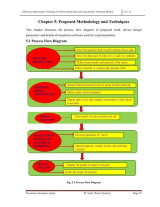
The conceptual explanation of various experiment and algorithms used has been already
covered in previous sections. Here simulation parameters are material, size, doping
concentration and work function. The performance evaluation parameters taken by different
authors are short circuit current, open circuit voltage, and power conversion efficiency and
fill factor. This section includes the various methodology used by research along with result
obtained. Advantages and limitation of a particular method also has been discussed in
following given comparison table:](https://image.slidesharecdn.com/divyashikha-210715045210/85/Efficiency-Improvement-Technique-for-silicon-based-Solar-cell-using-Surface-texturing-Method-39-320.jpg)
![Efficiency Improvement Technique for Silicon based Solar cell using Surface Texturing Method 2017-18
Poornima University, Jaipur M. Tech. (Power System) Page 28
2.4 Strengths and Weaknesses of Research Works Reviewed
After, the review of 26 research papers in the field of Efficiency Improvement Technique
for Silicon based Solar cell using Surface Texturing Method. Then there were a strengths
and weaknesses of different approaches to solve the issues discussed in previous chapters.
This chapter will enlist the strengths and weaknesses of the different methods used.
2.4.1 Strengths
Reactive ion etching process for three structures of the surface texture, i.e. structures
with column, hole structures and without mask texturing, having a measured
reflection of less than 0.4, 6.8% and 1.4% at wavelengths of 400 nm to 1000 nm [1].
Surface texture structure of GaAs photovoltaic V-trench has improved the
efficiency of 2.12%, and the quality of the device performance is about 9% [5].
Front surface texturing anti-reflective layer obtained by oxidation of silicon, which
leads to the reduction of reflection less than 5% [7].
The acidic etched surface of the plane (111) which has a higher density relative to
that of the plane (100) was exposed and leads to an increase in the number of small
pyramids per unit area of the surface of the wafer. The pyramids of alkaline and
acid surfaces have dimensions of 7-10 and 3-4 mm. As a result, pyramids in the acid
etch surface are larger than 50% smaller [8].
Acid etched surface capable of absorbing 0.87% of incident light from the surface
etched with an alkali, the average incident light of 300 to 1100 nm [8].
Optimum HF acid etching ratio: HNO3: H2O = 15: 1: 2.5 with etching time of 60
seconds and lowering 42.7% of reflectance value improves 112.4% of conversion
efficiency of the solar cell developed [11].
HF/HNO3/H2O acid solution for texturing mc-Si cells. The conversion efficiency of
the mc-Si solar cells, textured with the solution (HF/HNO3/H2O=30:1:2.5) has a
relatively high [18].
The solar cell with a CAE/RIE combined two-step textured structure showed the
highest efficiency at 17.78%. It also had a Jsc of 37.46mA/cm2
, Voc of 0.614 V, and
FF of 77.34% [19].](https://image.slidesharecdn.com/divyashikha-210715045210/85/Efficiency-Improvement-Technique-for-silicon-based-Solar-cell-using-Surface-texturing-Method-41-320.jpg)
![Efficiency Improvement Technique for Silicon based Solar cell using Surface Texturing Method 2017-18
Poornima University, Jaipur M. Tech. (Power System) Page 29
The forward light scattering enhanced scattering light in a forward direction was
enhanced by the AgNPs in the silicon and also improves the Jsc from 22.23 to
23.81mA/cm2
, which leads to the improvement of the cells efficiency from 8.7 to
10. 0% of [22].
The efficiency of the nano-textured cells improves in the range of 18.4 to 18.9%
because of the different wafers qualities from the bottom to the top of the Qsc-Si bar
and the difference between the colors of the Qsc-Si cells were depressed [24].
2.4.2 Weaknesses
The size of the surface texture pyramid decreases by less than 1µm or greater than
12µm, adversely affecting the light reflection, operating time and productivity of
heterojunction solar cells [2].
Implantation of hydrogen ions to produce only the textures of the silicon surface,
generally low density packaging, and a small proportional amount, are not effective
in suppressing the reflection of light Si [10].
Si has a high refractive index that reflects more than 35% of the infrared to
ultraviolet light of a polished Si surface [10].
Alkaline etchant cannot produce a uniform textured surface to generate sufficient
open circuit voltage (VOC) and high efficiency of mc-Si due to the unavoidable grain
randomly oriented with higher steps formed during the etching process [11].
In order to improve the absorption of incident light, is extensively used isotropic
texture, using nitric acid (HNO3), hydrofluoric acid (HF) and demineralized water
(DI H2O), but leads to an engraving of the pit of the grain boundary, [12]
Multicrystalline silicon solar cells can hardly be formed by alkaline etching because
the grains of the substrates are oriented randomly [18].
The solar cell with a CAE/ACE combined two-step textured structure showed
lowest surface reflectance, it also had the lowest efficiency at 15.83% [19].
2.5 Gaps in the Published Research
After reading 26 research papers some gaps have been identified in this research work are
listed below:](https://image.slidesharecdn.com/divyashikha-210715045210/85/Efficiency-Improvement-Technique-for-silicon-based-Solar-cell-using-Surface-texturing-Method-42-320.jpg)
![Efficiency Improvement Technique for Silicon based Solar cell using Surface Texturing Method 2017-18
Poornima University, Jaipur M. Tech. (Power System) Page 48
surfaces with changes in corrosion time. It can be seen that pyramids formation with time
of corrosion. For example, after 5 minutes, the pyramid began to show; after 15 minutes,
the surface of silicon is covered with small pyramids, and several have begun to grow; after
30 minutes, the silicon surface covered with pyramids. The reflectivity of mono-crystalline
silicon wafer after different corrosion time in the visible (450-1000nm), the reflection
decreases with rising corrosion time and the lowest reflectivity is 11%. For the corrosion
time, it is of the order of 25-45minutes, the corresponding reflectance is 11-15%. If the
etching time increases again, there is no large change in reflectivity.
4.1.2 Surface Textured for Polycrystalline Silicon
For monocrystalline silicon with a <100> orientation, the ideal pyramidal structure can be
etched with NaOH solution. However, for polysilicon, only a very small portion of the
surface is covered with an orientation (100), so that the use of anisotropic etching for a
textured surface is not feasible. Since the orientations of the polysilicon grains are arbitrary
and the alkaline solutions such as KOH or NaOH are anisotropic etchings, these can easily
lead to uneven texture, this alkaline etching method is not suitable for polysilicon texturing.
In terms of optics, the acid solution (the mixture of HF, H2O and HNO3) and the RIE
(reactive ion etching) method are isotropic surface texture methods for a textured
polysilicon surface. The acid etch solution for polysilicon is a mixture of HNO3,HF and
deionized water mixed by certain percentages, where HNO3 is used as a strong oxidizer, so
that the silicon becomes SiO2 after oxidation. The entire silicon surface is covered with a
dense SiO2 film after oxidation and this SiO2 film will protect the silicon from further
reaction. The HF solution is used as a complexing agent and this solution can dissolve the
SiO2 sheet, the resulting H2 [SiF6] complexes are soluble in water. H2 [SiF6] is a strong acid
stronger than sulfuric acid and easily dissociable in solution.
This reaction is therefore a positive feedback reaction, with the generation of H2 [SiF6] and
the dissociation of the increasing H+
concentration, then the rate of corrosion is also
increased. If the rate of corrosion is too fast, the reaction process is difficult to control,
resulting in poor corrosion. In order to reduce the corrosion reaction, by the law of mass
activity, the decrease in the HF concentration can slow down the reaction rate. The reaction
mechanism is as follows:](https://image.slidesharecdn.com/divyashikha-210715045210/85/Efficiency-Improvement-Technique-for-silicon-based-Solar-cell-using-Surface-texturing-Method-61-320.jpg)
![Efficiency Improvement Technique for Silicon based Solar cell using Surface Texturing Method 2017-18
Poornima University, Jaipur M. Tech. (Power System) Page 49
4HNO3+3Si =3SiO2+4NO ↑+2H2O+
6HF +SiO2= 2H2O+ H2[SiF6]
[SiF6]H2↔ [SiF6]2-
+2H+
Isotropic corrosion method of etching has nothing to do with the orientation of the grains,
because it will form a uniform textured surface on the surface of the polysilicon. The acid
etching process of polysilicon has several benefits: firstly, it can reduce the surface damage
layer and the surface of the texture for a very small period of time, which will save time for
manufacture; Second, after etching the surface is relatively flat and thin, which facilitates
the manufacture of a thin battery; Third, no NaOH solution is used to prevent
contamination by the Na ion; and the wafer after the acidic corrosion is flat, which
facilitates the formation of a relatively flat pn bond, thus contributing to improving the solar
cells stability; Finally, the flat surface is appropriate for the screen printing process and the
contact of the electrode is unlikely to break.
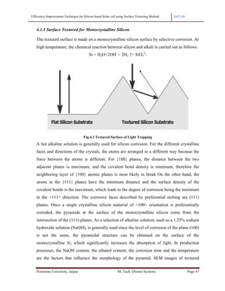
4.2 Optical Benefits of Textured Silicon
4.2.1 Front Reflectance Reduction
As a function of the wavelength, the reflection of normal light on the silicon surface is
determined by the complex refractive index nc = (n - ik) silicon and air:
R
n-a − n-1
?
n-a + n-1
?
4.1
In this case the subscript 0 and 1 for silicon and air respectively, where n is the real and k
is an imaginary part of the refractive index, depending on the wavelength. For air, as
convention n and k take the fix values of 1 and 0 respectively, thus:
R
na − 1 ?
+ ka
?
na + 1 ? + ka
?
4.2
There are two main solutions to reduce these front reflection losses in the solar cell: by an
anti-reflective coating (ARC) or by texturing the silicon surface, which will in most cases
be covered with ARC to further reduce the reflection on the front. In case of texture,](https://image.slidesharecdn.com/divyashikha-210715045210/85/Efficiency-Improvement-Technique-for-silicon-based-Solar-cell-using-Surface-texturing-Method-62-320.jpg)