SlideShare a Scribd company logo
1 of 3
Download to read offline
Nanoconstriction microscopy of the giant magnetoresistance
in cobalt/copper spin valves
S. J. C. H. Theeuwen, J. Caro, K. P. Wellock, and S. Radelaar
Delft Institute of Microelectronics and Submicron Technology (DIMES), Delft University
of Technology, Lorentzweg 1, 2628 CJ Delft, The Netherlands
C. H. Marrows and B. J. Hickey
Department of Physics and Astronomy, University of Leeds, Leeds LS2 9JT, United Kingdom
V. I. Kozub
A. F. Ioffe Physico-Technical Institute, St. Petersburg 194021, Russian Federation
͑Received 10 August 1999; accepted for publication 8 October 1999͒
We use nanometer-sized point contacts to a Co/Cu spin valve to study the giant magnetoresistance
͑GMR͒ of only a few Co domains. The measured data show strong device-to-device differences of
the GMR curve, which we attribute to the absence of averaging over many domains. The GMR ratio
decreases with increasing bias current. For one particular device, this is accompanied by the
development of two distinct GMR plateaus, the plateau level depending on bias polarity and sweep
direction of the magnetic field. We attribute the observed behavior to current-induced changes of the
magnetization, involving spin transfer due to incoherent emission of magnons and self-field effects.
© 1999 American Institute of Physics. ͓S0003-6951͑99͒01049-9͔
Currently, applications of the giant magnetoresistance
͑GMR͒ are realized, particularly in read heads for hard disks1
and magnetoresistive random access memories ͑MRAMs͒.2
These applications are based on the spin valve. This is a
trilayer structure, with a normal metal ͑NM͒ layer sand-
wiched between two ferromagnetic metal ͑FM͒ layers.3
The
spin-valve resistance depends strongly on the magnetic-field-
induced relative orientation of the magnetizations of the FM
layers. This GMR arises predominantly from spin-dependent
scattering of the electrons at the interfaces between the NM
and FM layers.1
So far, most spin-valve studies were performed on large
structures, up to millimeters wide. Since the domain size of a
FM film ranges from hundreds of nanometers to several mi-
crometers, the GMR arises from averaging over many do-
mains. Currently, emphasis shifts to spin valves patterned
into micrometer and submicrometer structures, entering the
regime of only a few domains. This has led, for example, to
the direct observation4
of the correlation of domain structure
and GMR and to very small memory elements for MRAMs.2
A very attractive way to enter the few-domain regime is
to use a point contact to a macroscopic spin valve. Such a
contact is a nanoconstriction between a metallic electrode
and the spin valve. When a current flows through the device,
the current density peaks strongly in the constriction ͑diam-
eter dϭ10–50 nm͒. As a result, in a resistance measurement
a hemispherical region of the spin valve is probed, in size
comparable to the constriction diameter ͓Fig. 1͑a͔͒. In this
region, only two domains are expected to contribute to the
GMR, one from each FM layer. Due to the minute layer
thickness ͑typically, several nanometers͒, the current flows
almost perpendicularly through the layers ͑CPP geometry͒,
as in the multilayer pillars of Gijs, Lenczowski, and
Giesbers5
and in the spin valves sandwiched between super-
conducting electrodes of Pratt et al.6
In this letter, we report
GMR measurements on Co/Cu spin-valve point contacts.
These devices work as a microscope, revealing effects of
only a few domains at the constriction. Further, the point-
contact geometry is very suitable to search for effects of
electron-spin transfer to the FM layers,7
either as predicted
by Slonczewski8
or by Kozub et al.9
We fabricate the spin valves on silicon membranes.10
On
the lower membrane face, a Cu͑2 nm͒/Co͑3 nm͒/Cu͑3.5 nm͒/
Co͑300 nm͒/Cu͑300 nm͒ structure is sputtered ͓Fig. 1͑a͔͒.
FIG. 1. Schematic cross-section of a spin-valve point contact ͑a͒ and GMR
of a 0.38 ⍀ contact, measured at Tϭ4.2 K with an in-plane field, for Iac
ϭ100 ␮A ͑b͒ and Ibiasϭ10 mA ͑c͒.
APPLIED PHYSICS LETTERS VOLUME 75, NUMBER 23 6 DECEMBER 1999
36770003-6951/99/75(23)/3677/3/$15.00 © 1999 American Institute of Physics
Downloaded 06 Jan 2004 to 145.94.80.165. Redistribution subject to AIP license or copyright, see http://ojps.aip.org/aplo/aplcr.jsp
The 2 nm Cu layer is a buffer and the 300 nm Cu cap shunts
any current-in-plane ͑CIP͒ series GMR of the trilayer film.11
The device is completed by etching a nanohole in the mem-
brane and deposition of Cu on the upper face, to fill the hole
and form the counter electrode. The different Co thicknesses
cause magnetization reversal of the layers at different fields.
We make identical layered films ͑but with a 3 nm cap͒ for
CIP control measurements. The point-contact resistances,
measured in a four-wire geometry, are in the range of
0.3–8 ⍀.
These spin valves exhibit a clear GMR. We observe sub-
stantial device-to-device differences in the GMR curve, at-
taining a maximum GMR ratio of 2% (ratioϭ⌬R/Rsat ; ⌬R
ϭR0ϪRsat , R0ϭmaximum resistance, Rsatϭsaturated resis-
tance͒. Step-like transitions in the GMR often occur. These
observations agree with the absence of averaging, as ex-
pected when only a few domains are probed. In general, the
GMR ratio decreases with increasing bias current. Contrary
to the point contacts, the CIP films do not exhibit a GMR.
This indicates that 300 nm Co is thick enough to shunt the
CIP GMR and that, consequently, the point-contact GMR
arises from the constriction region, where the current must
traverse the Co/Cu interfaces. The CIP films do show the
anisotropic magnetoresistance ͑AMR͒.12
The AMR of the
point contacts is negligible (AMRϽ0.1%). Its dependence
on the field orientation correlates in an AMR fashion with
the average current direction through the constriction ͑which
is along the constriction axis͒, from which it thus must origi-
nate. The point-contact spectra d2
I/dV2
(V) of the devices,
i.e., the voltage dependence of the second derivative of the
I–V curve, are featureless. This is unlike spectra of ballistic
contacts,13
which show phonon peaks, and unlike spectra of
multilayer contacts of Tsoi et al.,14
which show spin-wave
excitations. We conclude that electron transport in our con-
tacts is diffusive or between ballistic and diffusive.
This letter concentrates on one specific contact which
nicely illustrates the absence of averaging over the properties
of many domains. This contact has Rϭ0.38 ⍀, which corre-
sponds to a diameter of 50 nm,15
and a 1.2% GMR ratio at
4.2 K. This ratio is dominated by the contribution of the
thick Co layer to Rsat . After correction, an upper bound of
the intrinsic ratio is estimated at 5%. Figure 1͑b͒ shows the
GMR curve for the in-plane field geometry, measured at T
ϭ4.2 K and with low-level ac excitation (Iacϭ100 ␮A).
This curve is much narrower than the perpendicular-field
curve ͑not shown͒, in agreement with the shape anisotropy of
the layers. Coming from high field, the in-plane curve shows
a gradual increase before Hϭ0, a hysteretic maximum close
to Hϭ0, and a steep decrease to saturation at ␮0͉H͉
ϭ6 mT. This differs from the GMR of a multi-domain area
of a spin valve, which yields a maximum after Hϭ0 due to
hysteresis of the multi-domain system. The curve of Fig. 1͑b͒
reflects specific magnetization properties of just a few or
even two domains. The curve suggests a gradual change of
the magnetization of one domain to a preferential direction
when approaching Hϭ0 and an abrupt switching of the mag-
netization to a completely aligned state at ␮0͉H͉ϭ6 mT, in-
volving the other domain. The GMR in Fig. 1͑b͒ occurs at a
much lower field than those of Myers et al. for a very similar
device,7
fabricated with a pre-etched nanohole. This method,
contrary to ours, for hole sizes comparable to or larger than a
layer thickness, leads to strong topography at the hole after
deposition of the Cu electrode. Thus, the layers are distorted,
affecting the field scale.
At elevated bias currents the picture becomes more rich,
as illustrated in Fig. 1͑c͒ for Ibiasϭϩ10 mA ͑positive cur-
rent: electrons flow from the thin Co layer to the thick one͒.
Two pronounced resistance plateaus develop, their height de-
pending on the field-sweep direction and current polarity.
The upper plateau occurs when coming from positive H and
biasing with positive Ibias or from negative H and applying
negative Ibias . The lower plateau appears for a reversed-
sweep direction or opposite current polarity. Thus, one can
choose the relative magnetization direction of the domains
with the magnetic history and the current polarity. The gap
between the upper and lower plateau first opens and then
closes when the bias current is increased from 100 ␮A to 100
mA, reducing the GMR ratio by a factor of 6. This behavior
is plotted in Fig. 2, where R0 is the plateau level. The plotted
bias range corresponds to current densities up to 5
ϫ109
A/cm2
, i.e., 100 times higher than values in GMR read
heads.3
When converted to the GMR ratio, the lower branch
of R0 in Fig. 2 reaches its final level of 0.2% at 20 mA, while
the upper branch decreases approximately linearly across the
whole bias range. The plateaus are stable for many hours.
We never observed a spontaneous transition between them.
Further, the side of the gradual change of the GMR peak
broadens with increasing current, while the steep side is un-
affected. In Fig. 3 this is illustrated for one biasing and
sweeping combination.
Joule heating might be responsible for the above behav-
ior, in particular, the decrease of the GMR peak with increas-
FIG. 2. Dependences of R0 and Rsat on bias current, for the combinations of
sweep direction and current polarity, for the in-plane field geometry and T
ϭ4.2 K. The opening and closing of a gap between plateaus can be seen.
Lines guide the eye.
FIG. 3. GMR for different positive currents. Tϭ4.2 K. The arrow indicates
the sweep direction. For high currents, the GMR is reduced and broadened
on one side. The inset shows the temperature dependence of the GMR ratio.
3678 Appl. Phys. Lett., Vol. 75, No. 23, 6 December 1999 Theeuwen et al.
Downloaded 06 Jan 2004 to 145.94.80.165. Redistribution subject to AIP license or copyright, see http://ojps.aip.org/aplo/aplcr.jsp
ing current and its broadening. To check this, we measure
the temperature dependence ͑1.5–293 K͒ of the zero-bias
(Iacϭ100 ␮A) GMR curve, yielding a constant GMR ratio
up to 100 K and a decrease to 0.6% at 293 K ͑inset, Fig. 3͒.
Further, with increasing temperature the gradual side of the
GMR curve is hardly affected, while the steep side shifts
towards Hϭ0. This is contrary to the bias dependence, so
that Joule heating is clearly excluded. The zero-field resis-
tance R0(Tϭ4.2 K, Ibias) decreases in the range 0–50 mA,
whereafter it increases ͑Fig. 2͒. Again, this differs from the
measured R0(T,Iacϭ100 ␮A), which increases monoto-
nously. The measured bias dependence Rsat(Tϭ4.2 K, Ibias)
also shows a monotonic increase. We attribute the latter in-
crease to extra scattering due to phonon and magnon creation
enabled by a bias-induced nonequilibrium electron-
distribution function. The resulting resistance increase also
contributes to R0(Tϭ4.2 K, Ibias). However, we argue that
below 50 mA R0(Tϭ4.2 K,Ibias) is dominated by another
effect, viz. current-induced magnetization changes. These
arise from the self-field ͑i.e., the field generated by the cur-
rent according to Ampe`re’s law͒ or from spin transfer to the
FM layers. Spin transfer leads to coherent rotation of the
magnetization,8
resulting in switching of the resistance,7
or
to incoherent emission of magnons,9
as discussed below.
We estimate the self-field by approximating the point
contact by a hyperboloid of revolution.16
For Iϭ5 mA, the
maximum of ␮0Hself in the thin ͑thick͒ Co layer is 24 ͑12͒
mT. This is comparable to the field scale of the zero-bias
GMR. Thus, the self-field should affect the GMR for most of
the bias range. For example, it should broaden the GMR
peak. Broadening is indeed observed for the gradual side of
the peak, but the steep side is unaffected. Apparently, other
and stronger driving forces dominate certain features of the
GMR, for example, a uniaxial anisotropy induced by
fabrication-related effects. This, combined with the self-field,
which depending on the bias polarity, can guide the magne-
tization in either direction of the anisotropy axis and can give
rise to plateaus. With increasing bias, the self-field will tend
to impose a vortex character upon the magnetization of both
Co layers, eventually leading to almost congruent vortices in
the Co layers, and consequently, a reduction of the GMR,
which is what we observe.
Spin transfer influences the thin Co layer much more
than the thick Co layer, since the latter is strongly exchange
coupled to its surroundings.8
According to the coherent rota-
tion model,8
the magnetization of the thin layer, and thus the
magnetoresistance, should switch abruptly at a threshold cur-
rent. Our contacts do not show switching, apparently exclud-
ing this mechanism. Rather, the GMR evolves gradually with
bias. This can be explained9
by incoherent emission of non-
equilibrium magnons, giving rise to a magnon ‘‘hot spot’’ in
the thin Co layer, characterized by an effective magnon tem-
perature Tm . Since the probability of electron–magnon cre-
ation ͑a spin-flip process͒ is proportional to the density of
final electron states, which in turn is spin dependent, Tm
depends on the current polarity and the relative orientation of
the magnetizations of the layers, angles close to 0° or 180°
favoring high Tm . Further, Tm is proportional to the bias.
Deviations of the magnetization of the thin layer from a pref-
erential direction are assumed to be thermally activated by
Tm . Apart from a gradual decrease of the GMR with current,
this model also gives a current-direction-dependent GMR
plateau. However, the plateau level does not depend on the
sweep direction, contrary to the measurements. This indi-
cates that the model in its present form does not catch all
magnetic ingredients of the spin valve. In addition, a com-
plete treatment should include the interplay of spin transfer
and the self-field effect. Similar to the Slonczewski’s spin
transfer, also the spin-transfer effect put forward here can be
used to set the bits of a MRAM, but with the additional
advantage of write capability for parallel and antiparallel ori-
entations of the magnetizations.
In conclusion, using Co/Cu spin-valve point contacts, we
have studied the CPP GMR of only a few domains. Due to
the absence of averaging over many domains, the GMR
curve shows strong device-to-device differences, the maxi-
mum GMR ratio being 2%. For one device we studied in
detail the dependence of the GMR curve on the bias current
up to 100 mA and at a temperature up to 293 K. The GMR
ratio decreases with increasing bias, while two distinct GMR
plateaus develop around Hϭ0. We attribute this behavior to
current-induced changes of the magnetization, involving spin
transfer due to incoherent emission of magnons and self-field
effects, while we exclude Joule heating.
The authors gratefully acknowledge G. E. W. Bauer, R.
P. van Gorkom, and T. M. Klapwijk for stimulating discus-
sions and N. N. Gribov for expert support in preparing Si
membranes.
1
See the collection of articles in IBM J. Res. Dev. 42, ͑1998͒.
2
S. Tehrani, E. Chen, M. Durlam, M. DeHerrera, J. M. Slaughter, J. Shi,
and G. Kerszykowski, J. Appl. Phys. 85, 5822 ͑1999͒.
3
For a review on spin valves, see B. Dieny, J. Magn. Magn. Mater. 136,
335 ͑1994͒.
4
X. Portier, E. Yu. Tsymbal, A. K. Petford-Long, T. C. Anthony, and J. A.
Brug, Phys. Rev. B 58, R591 ͑1998͒.
5
M. A. M. Gijs, S. K. J. Lenczowski, and J. B. Giesbers, Phys. Rev. Lett.
70, 3343 ͑1993͒.
6
W. P. Pratt Jr., S. D. Steenwyk, S. Y. Hsu, W.-C. Chiang, A. C. Schaefer,
R. Loloee, and J. Bass, IEEE Trans. Magn. MAG-33, 3505 ͑1997͒.
7
E. B. Myers, D. C. Ralph, J. A. Katine, R. N. Louie, and R. A. Buhrman,
Science 285, 867 ͑1999͒.
8
J. C. Slonczewski, J. Magn. Magn. Mater. 159, L1 ͑1996͒; 195, L261
͑1999͒.
9
V. I. Kozub et al. ͑unpublished͒.
10
N. N. Gribov, S. J. C. H. Theeuwen, J. Caro, E. van der Drift, F. D.
Tichelaar, T. R. de Kruijff, and B. J. Hickey, J. Vac. Sci. Technol. B 16,
3943 ͑1998͒.
11
K. P. Wellock, S. J. C. H. Theeuwen, J. Caro, N. N. Gribov, R. P. van
Gorkom, S. Radelaar, F. D. Tichelaar, B. J. Hickey, and C. H. Marrows,
Phys. Rev. B 60, 10291 ͑1999͒.
12
T. R. McGuire and R. I. Potter, IEEE Trans. Magn. MAG-11, 1018
͑1975͒.
13
P. A. M. Holweg, J. Caro, A. H. Verbruggen, and S. Radelaar, Phys. Rev.
B 45, 9311 ͑1992͒.
14
M. Tsoi, A. G. M. Jansen, J. Bass, W.-C. Chiang, M. Seck, V. Tsoi, and
P. Wyder, Phys. Rev. Lett. 80, 4281 ͑1998͒.
15
For our layers ␳Co /␳CuϷ8. Thus, neglecting interface resistances, the Co
layers dominate the resistance, so that to a good approximation the resis-
tance is the Maxwell resistance: RϷ␳Co/4a. The value ␳Ca(4.2 K)
ϭ40 n⍀m then gives 2aϷ50 nm, in agreement with the lithographic size.
16
We apply Ampe`re’s law to the hyperboloid geometry ͓L. K. J. Van-
damme, Appl. Phys. 11, 89 ͑1976͔͒, using the oblate spherical coordinates
␩ and ␰. This yields the ͑by nature inhomogeneous͒ self-field ␮0Hself
ϭF(␩,␰)(␮0Ibias/2␲a). The maximum value of the spatial function
F(␩,␰) in the thin ͑thick͒ Co layers at the constriction is 0.6 ͑0.3͒.
3679Appl. Phys. Lett., Vol. 75, No. 23, 6 December 1999 Theeuwen et al.
Downloaded 06 Jan 2004 to 145.94.80.165. Redistribution subject to AIP license or copyright, see http://ojps.aip.org/aplo/aplcr.jsp

More Related Content

What's hot

Dam Health assessment using geophysics.
Dam Health assessment using geophysics.Dam Health assessment using geophysics.
Dam Health assessment using geophysics.shubham shukla
 
Application of vertical electrical sounding and horizontal profiling methods ...
Application of vertical electrical sounding and horizontal profiling methods ...Application of vertical electrical sounding and horizontal profiling methods ...
Application of vertical electrical sounding and horizontal profiling methods ...Alexander Decker
 
Quartz Crystal Microbalance QCM - Theory and Modeling
Quartz Crystal Microbalance QCM - Theory and ModelingQuartz Crystal Microbalance QCM - Theory and Modeling
Quartz Crystal Microbalance QCM - Theory and ModelingMarco Mauro
 
Electrical Resistivity Survey Forground Water At Eye Zheba Village, Off Bida ...
Electrical Resistivity Survey Forground Water At Eye Zheba Village, Off Bida ...Electrical Resistivity Survey Forground Water At Eye Zheba Village, Off Bida ...
Electrical Resistivity Survey Forground Water At Eye Zheba Village, Off Bida ...iosrjce
 
Electrical resistivity and electromagnetic method for detection of water bear...
Electrical resistivity and electromagnetic method for detection of water bear...Electrical resistivity and electromagnetic method for detection of water bear...
Electrical resistivity and electromagnetic method for detection of water bear...shubham shukla
 
AME441AL_Final_Report
AME441AL_Final_ReportAME441AL_Final_Report
AME441AL_Final_ReportMatt Tonokawa
 
Geprags strain controlled magnetic science_direct_2014
Geprags strain controlled magnetic science_direct_2014Geprags strain controlled magnetic science_direct_2014
Geprags strain controlled magnetic science_direct_2014Phạm Công
 

What's hot (15)

Resistivity Survey
Resistivity SurveyResistivity Survey
Resistivity Survey
 
sheet resistivity
sheet resistivitysheet resistivity
sheet resistivity
 
Report on diffusion
Report on diffusionReport on diffusion
Report on diffusion
 
Laterologs
LaterologsLaterologs
Laterologs
 
Dam Health assessment using geophysics.
Dam Health assessment using geophysics.Dam Health assessment using geophysics.
Dam Health assessment using geophysics.
 
Resistivity method
Resistivity method Resistivity method
Resistivity method
 
sheet-resistance-measurement
sheet-resistance-measurementsheet-resistance-measurement
sheet-resistance-measurement
 
Los Alamos Paper
Los Alamos PaperLos Alamos Paper
Los Alamos Paper
 
Application of vertical electrical sounding and horizontal profiling methods ...
Application of vertical electrical sounding and horizontal profiling methods ...Application of vertical electrical sounding and horizontal profiling methods ...
Application of vertical electrical sounding and horizontal profiling methods ...
 
Quartz Crystal Microbalance QCM - Theory and Modeling
Quartz Crystal Microbalance QCM - Theory and ModelingQuartz Crystal Microbalance QCM - Theory and Modeling
Quartz Crystal Microbalance QCM - Theory and Modeling
 
Electrical Resistivity Survey Forground Water At Eye Zheba Village, Off Bida ...
Electrical Resistivity Survey Forground Water At Eye Zheba Village, Off Bida ...Electrical Resistivity Survey Forground Water At Eye Zheba Village, Off Bida ...
Electrical Resistivity Survey Forground Water At Eye Zheba Village, Off Bida ...
 
Electrical resistivity and electromagnetic method for detection of water bear...
Electrical resistivity and electromagnetic method for detection of water bear...Electrical resistivity and electromagnetic method for detection of water bear...
Electrical resistivity and electromagnetic method for detection of water bear...
 
AME441AL_Final_Report
AME441AL_Final_ReportAME441AL_Final_Report
AME441AL_Final_Report
 
conventional resistivity logs
conventional resistivity logsconventional resistivity logs
conventional resistivity logs
 
Geprags strain controlled magnetic science_direct_2014
Geprags strain controlled magnetic science_direct_2014Geprags strain controlled magnetic science_direct_2014
Geprags strain controlled magnetic science_direct_2014
 

Similar to APL

Effect of ac driving current on magnetoimpedance effect aragoneses 2000
Effect of ac driving current on magnetoimpedance effect aragoneses 2000Effect of ac driving current on magnetoimpedance effect aragoneses 2000
Effect of ac driving current on magnetoimpedance effect aragoneses 2000Smith Arauco Canchumuni
 
Enhanced Exchange Pinning Field For Fe Mn Spin Valves
Enhanced Exchange Pinning Field For Fe Mn Spin ValvesEnhanced Exchange Pinning Field For Fe Mn Spin Valves
Enhanced Exchange Pinning Field For Fe Mn Spin Valvesguestc57e7ed
 
Enhanced Exchange Pinning Field For Fe Mn Spin Valves
Enhanced Exchange Pinning Field For Fe Mn Spin ValvesEnhanced Exchange Pinning Field For Fe Mn Spin Valves
Enhanced Exchange Pinning Field For Fe Mn Spin Valvesguestc57e7ed
 
HFSS ANTENNA FOR KU BAND WITH DEFECTED GROUND STRUCTURES
HFSS ANTENNA FOR KU BAND WITH DEFECTED GROUND STRUCTURESHFSS ANTENNA FOR KU BAND WITH DEFECTED GROUND STRUCTURES
HFSS ANTENNA FOR KU BAND WITH DEFECTED GROUND STRUCTURESAKSHAT GANGWAR
 
2001 field based scanning tunneling microscope manipulation of antimony dimer...
2001 field based scanning tunneling microscope manipulation of antimony dimer...2001 field based scanning tunneling microscope manipulation of antimony dimer...
2001 field based scanning tunneling microscope manipulation of antimony dimer...pmloscholte
 
1998 epitaxial film growth of the charge density-wave conductor rb0.30 moo3 o...
1998 epitaxial film growth of the charge density-wave conductor rb0.30 moo3 o...1998 epitaxial film growth of the charge density-wave conductor rb0.30 moo3 o...
1998 epitaxial film growth of the charge density-wave conductor rb0.30 moo3 o...pmloscholte
 
Giant magnetoresistance ppt
Giant magnetoresistance pptGiant magnetoresistance ppt
Giant magnetoresistance ppttedoado
 
Exploration Geophysics III semester.pdf
Exploration Geophysics III semester.pdfExploration Geophysics III semester.pdf
Exploration Geophysics III semester.pdfSHAHEENAKBAR3
 
Al gan ultraviolet photodetectors grown by molecular beam epitaxy on si(111) ...
Al gan ultraviolet photodetectors grown by molecular beam epitaxy on si(111) ...Al gan ultraviolet photodetectors grown by molecular beam epitaxy on si(111) ...
Al gan ultraviolet photodetectors grown by molecular beam epitaxy on si(111) ...Kal Tar
 
MPC 1 exam june 2022 marking key.pdf
MPC 1 exam june 2022 marking key.pdfMPC 1 exam june 2022 marking key.pdf
MPC 1 exam june 2022 marking key.pdfDavy40
 

Similar to APL (20)

PRB_wellock_1999
PRB_wellock_1999PRB_wellock_1999
PRB_wellock_1999
 
Giant magnetoresistance
Giant magnetoresistanceGiant magnetoresistance
Giant magnetoresistance
 
Effect of ac driving current on magnetoimpedance effect aragoneses 2000
Effect of ac driving current on magnetoimpedance effect aragoneses 2000Effect of ac driving current on magnetoimpedance effect aragoneses 2000
Effect of ac driving current on magnetoimpedance effect aragoneses 2000
 
666.full
666.full666.full
666.full
 
Enhanced Exchange Pinning Field For Fe Mn Spin Valves
Enhanced Exchange Pinning Field For Fe Mn Spin ValvesEnhanced Exchange Pinning Field For Fe Mn Spin Valves
Enhanced Exchange Pinning Field For Fe Mn Spin Valves
 
Enhanced Exchange Pinning Field For Fe Mn Spin Valves
Enhanced Exchange Pinning Field For Fe Mn Spin ValvesEnhanced Exchange Pinning Field For Fe Mn Spin Valves
Enhanced Exchange Pinning Field For Fe Mn Spin Valves
 
Oil gas seabed logging
Oil gas seabed loggingOil gas seabed logging
Oil gas seabed logging
 
HFSS ANTENNA FOR KU BAND WITH DEFECTED GROUND STRUCTURES
HFSS ANTENNA FOR KU BAND WITH DEFECTED GROUND STRUCTURESHFSS ANTENNA FOR KU BAND WITH DEFECTED GROUND STRUCTURES
HFSS ANTENNA FOR KU BAND WITH DEFECTED GROUND STRUCTURES
 
Eg35750753
Eg35750753Eg35750753
Eg35750753
 
2001 field based scanning tunneling microscope manipulation of antimony dimer...
2001 field based scanning tunneling microscope manipulation of antimony dimer...2001 field based scanning tunneling microscope manipulation of antimony dimer...
2001 field based scanning tunneling microscope manipulation of antimony dimer...
 
JAP-Avril02_SALAHUN
JAP-Avril02_SALAHUNJAP-Avril02_SALAHUN
JAP-Avril02_SALAHUN
 
1998 epitaxial film growth of the charge density-wave conductor rb0.30 moo3 o...
1998 epitaxial film growth of the charge density-wave conductor rb0.30 moo3 o...1998 epitaxial film growth of the charge density-wave conductor rb0.30 moo3 o...
1998 epitaxial film growth of the charge density-wave conductor rb0.30 moo3 o...
 
Giant magnetoresistance ppt
Giant magnetoresistance pptGiant magnetoresistance ppt
Giant magnetoresistance ppt
 
Oe3424742482
Oe3424742482Oe3424742482
Oe3424742482
 
Exploration Geophysics III semester.pdf
Exploration Geophysics III semester.pdfExploration Geophysics III semester.pdf
Exploration Geophysics III semester.pdf
 
Electrical method
Electrical methodElectrical method
Electrical method
 
Al gan ultraviolet photodetectors grown by molecular beam epitaxy on si(111) ...
Al gan ultraviolet photodetectors grown by molecular beam epitaxy on si(111) ...Al gan ultraviolet photodetectors grown by molecular beam epitaxy on si(111) ...
Al gan ultraviolet photodetectors grown by molecular beam epitaxy on si(111) ...
 
Line width
Line widthLine width
Line width
 
MPC 1 exam june 2022 marking key.pdf
MPC 1 exam june 2022 marking key.pdfMPC 1 exam june 2022 marking key.pdf
MPC 1 exam june 2022 marking key.pdf
 
AFMC Physics 2006
AFMC Physics  2006AFMC Physics  2006
AFMC Physics 2006
 

More from Steven Theeuwen

EDL2003_RF power silicon-on-glass VDMOSFET
EDL2003_RF power silicon-on-glass VDMOSFETEDL2003_RF power silicon-on-glass VDMOSFET
EDL2003_RF power silicon-on-glass VDMOSFETSteven Theeuwen
 
High Efficiency LDMOS Technology for UMTS base stations_journal
High Efficiency LDMOS Technology for UMTS base stations_journalHigh Efficiency LDMOS Technology for UMTS base stations_journal
High Efficiency LDMOS Technology for UMTS base stations_journalSteven Theeuwen
 
A 72% PAE, 10-Watt, CMOS-LDMOS Switch-Mode Power Amplifier for Sub-1GHz Appli...
A 72% PAE, 10-Watt, CMOS-LDMOS Switch-Mode Power Amplifier for Sub-1GHz Appli...A 72% PAE, 10-Watt, CMOS-LDMOS Switch-Mode Power Amplifier for Sub-1GHz Appli...
A 72% PAE, 10-Watt, CMOS-LDMOS Switch-Mode Power Amplifier for Sub-1GHz Appli...Steven Theeuwen
 
LDMOS Ruggedness Reliability Microwave Journal
LDMOS Ruggedness Reliability Microwave JournalLDMOS Ruggedness Reliability Microwave Journal
LDMOS Ruggedness Reliability Microwave JournalSteven Theeuwen
 
IEDM2006_Efficiency improvement
IEDM2006_Efficiency improvementIEDM2006_Efficiency improvement
IEDM2006_Efficiency improvementSteven Theeuwen
 
S-Band Radar LDMOS Transistors EuMW2009
S-Band Radar LDMOS Transistors EuMW2009S-Band Radar LDMOS Transistors EuMW2009
S-Band Radar LDMOS Transistors EuMW2009Steven Theeuwen
 
High_Voltage_RF_LDMOS_Technology_for_Broadcast_Applications_pub
High_Voltage_RF_LDMOS_Technology_for_Broadcast_Applications_pubHigh_Voltage_RF_LDMOS_Technology_for_Broadcast_Applications_pub
High_Voltage_RF_LDMOS_Technology_for_Broadcast_Applications_pubSteven Theeuwen
 
LDMOS technology for RF power amplifiers
LDMOS technology for RF power amplifiersLDMOS technology for RF power amplifiers
LDMOS technology for RF power amplifiersSteven Theeuwen
 

More from Steven Theeuwen (10)

EDL2003_RF power silicon-on-glass VDMOSFET
EDL2003_RF power silicon-on-glass VDMOSFETEDL2003_RF power silicon-on-glass VDMOSFET
EDL2003_RF power silicon-on-glass VDMOSFET
 
High Efficiency LDMOS Technology for UMTS base stations_journal
High Efficiency LDMOS Technology for UMTS base stations_journalHigh Efficiency LDMOS Technology for UMTS base stations_journal
High Efficiency LDMOS Technology for UMTS base stations_journal
 
SJCH_Theeuwen_Thesis
SJCH_Theeuwen_ThesisSJCH_Theeuwen_Thesis
SJCH_Theeuwen_Thesis
 
A 72% PAE, 10-Watt, CMOS-LDMOS Switch-Mode Power Amplifier for Sub-1GHz Appli...
A 72% PAE, 10-Watt, CMOS-LDMOS Switch-Mode Power Amplifier for Sub-1GHz Appli...A 72% PAE, 10-Watt, CMOS-LDMOS Switch-Mode Power Amplifier for Sub-1GHz Appli...
A 72% PAE, 10-Watt, CMOS-LDMOS Switch-Mode Power Amplifier for Sub-1GHz Appli...
 
mwj201012-RF Lighting
mwj201012-RF Lightingmwj201012-RF Lighting
mwj201012-RF Lighting
 
LDMOS Ruggedness Reliability Microwave Journal
LDMOS Ruggedness Reliability Microwave JournalLDMOS Ruggedness Reliability Microwave Journal
LDMOS Ruggedness Reliability Microwave Journal
 
IEDM2006_Efficiency improvement
IEDM2006_Efficiency improvementIEDM2006_Efficiency improvement
IEDM2006_Efficiency improvement
 
S-Band Radar LDMOS Transistors EuMW2009
S-Band Radar LDMOS Transistors EuMW2009S-Band Radar LDMOS Transistors EuMW2009
S-Band Radar LDMOS Transistors EuMW2009
 
High_Voltage_RF_LDMOS_Technology_for_Broadcast_Applications_pub
High_Voltage_RF_LDMOS_Technology_for_Broadcast_Applications_pubHigh_Voltage_RF_LDMOS_Technology_for_Broadcast_Applications_pub
High_Voltage_RF_LDMOS_Technology_for_Broadcast_Applications_pub
 
LDMOS technology for RF power amplifiers
LDMOS technology for RF power amplifiersLDMOS technology for RF power amplifiers
LDMOS technology for RF power amplifiers
 

APL

  • 1. Nanoconstriction microscopy of the giant magnetoresistance in cobalt/copper spin valves S. J. C. H. Theeuwen, J. Caro, K. P. Wellock, and S. Radelaar Delft Institute of Microelectronics and Submicron Technology (DIMES), Delft University of Technology, Lorentzweg 1, 2628 CJ Delft, The Netherlands C. H. Marrows and B. J. Hickey Department of Physics and Astronomy, University of Leeds, Leeds LS2 9JT, United Kingdom V. I. Kozub A. F. Ioffe Physico-Technical Institute, St. Petersburg 194021, Russian Federation ͑Received 10 August 1999; accepted for publication 8 October 1999͒ We use nanometer-sized point contacts to a Co/Cu spin valve to study the giant magnetoresistance ͑GMR͒ of only a few Co domains. The measured data show strong device-to-device differences of the GMR curve, which we attribute to the absence of averaging over many domains. The GMR ratio decreases with increasing bias current. For one particular device, this is accompanied by the development of two distinct GMR plateaus, the plateau level depending on bias polarity and sweep direction of the magnetic field. We attribute the observed behavior to current-induced changes of the magnetization, involving spin transfer due to incoherent emission of magnons and self-field effects. © 1999 American Institute of Physics. ͓S0003-6951͑99͒01049-9͔ Currently, applications of the giant magnetoresistance ͑GMR͒ are realized, particularly in read heads for hard disks1 and magnetoresistive random access memories ͑MRAMs͒.2 These applications are based on the spin valve. This is a trilayer structure, with a normal metal ͑NM͒ layer sand- wiched between two ferromagnetic metal ͑FM͒ layers.3 The spin-valve resistance depends strongly on the magnetic-field- induced relative orientation of the magnetizations of the FM layers. This GMR arises predominantly from spin-dependent scattering of the electrons at the interfaces between the NM and FM layers.1 So far, most spin-valve studies were performed on large structures, up to millimeters wide. Since the domain size of a FM film ranges from hundreds of nanometers to several mi- crometers, the GMR arises from averaging over many do- mains. Currently, emphasis shifts to spin valves patterned into micrometer and submicrometer structures, entering the regime of only a few domains. This has led, for example, to the direct observation4 of the correlation of domain structure and GMR and to very small memory elements for MRAMs.2 A very attractive way to enter the few-domain regime is to use a point contact to a macroscopic spin valve. Such a contact is a nanoconstriction between a metallic electrode and the spin valve. When a current flows through the device, the current density peaks strongly in the constriction ͑diam- eter dϭ10–50 nm͒. As a result, in a resistance measurement a hemispherical region of the spin valve is probed, in size comparable to the constriction diameter ͓Fig. 1͑a͔͒. In this region, only two domains are expected to contribute to the GMR, one from each FM layer. Due to the minute layer thickness ͑typically, several nanometers͒, the current flows almost perpendicularly through the layers ͑CPP geometry͒, as in the multilayer pillars of Gijs, Lenczowski, and Giesbers5 and in the spin valves sandwiched between super- conducting electrodes of Pratt et al.6 In this letter, we report GMR measurements on Co/Cu spin-valve point contacts. These devices work as a microscope, revealing effects of only a few domains at the constriction. Further, the point- contact geometry is very suitable to search for effects of electron-spin transfer to the FM layers,7 either as predicted by Slonczewski8 or by Kozub et al.9 We fabricate the spin valves on silicon membranes.10 On the lower membrane face, a Cu͑2 nm͒/Co͑3 nm͒/Cu͑3.5 nm͒/ Co͑300 nm͒/Cu͑300 nm͒ structure is sputtered ͓Fig. 1͑a͔͒. FIG. 1. Schematic cross-section of a spin-valve point contact ͑a͒ and GMR of a 0.38 ⍀ contact, measured at Tϭ4.2 K with an in-plane field, for Iac ϭ100 ␮A ͑b͒ and Ibiasϭ10 mA ͑c͒. APPLIED PHYSICS LETTERS VOLUME 75, NUMBER 23 6 DECEMBER 1999 36770003-6951/99/75(23)/3677/3/$15.00 © 1999 American Institute of Physics Downloaded 06 Jan 2004 to 145.94.80.165. Redistribution subject to AIP license or copyright, see http://ojps.aip.org/aplo/aplcr.jsp
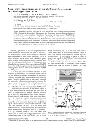
  • 2. The 2 nm Cu layer is a buffer and the 300 nm Cu cap shunts any current-in-plane ͑CIP͒ series GMR of the trilayer film.11 The device is completed by etching a nanohole in the mem- brane and deposition of Cu on the upper face, to fill the hole and form the counter electrode. The different Co thicknesses cause magnetization reversal of the layers at different fields. We make identical layered films ͑but with a 3 nm cap͒ for CIP control measurements. The point-contact resistances, measured in a four-wire geometry, are in the range of 0.3–8 ⍀. These spin valves exhibit a clear GMR. We observe sub- stantial device-to-device differences in the GMR curve, at- taining a maximum GMR ratio of 2% (ratioϭ⌬R/Rsat ; ⌬R ϭR0ϪRsat , R0ϭmaximum resistance, Rsatϭsaturated resis- tance͒. Step-like transitions in the GMR often occur. These observations agree with the absence of averaging, as ex- pected when only a few domains are probed. In general, the GMR ratio decreases with increasing bias current. Contrary to the point contacts, the CIP films do not exhibit a GMR. This indicates that 300 nm Co is thick enough to shunt the CIP GMR and that, consequently, the point-contact GMR arises from the constriction region, where the current must traverse the Co/Cu interfaces. The CIP films do show the anisotropic magnetoresistance ͑AMR͒.12 The AMR of the point contacts is negligible (AMRϽ0.1%). Its dependence on the field orientation correlates in an AMR fashion with the average current direction through the constriction ͑which is along the constriction axis͒, from which it thus must origi- nate. The point-contact spectra d2 I/dV2 (V) of the devices, i.e., the voltage dependence of the second derivative of the I–V curve, are featureless. This is unlike spectra of ballistic contacts,13 which show phonon peaks, and unlike spectra of multilayer contacts of Tsoi et al.,14 which show spin-wave excitations. We conclude that electron transport in our con- tacts is diffusive or between ballistic and diffusive. This letter concentrates on one specific contact which nicely illustrates the absence of averaging over the properties of many domains. This contact has Rϭ0.38 ⍀, which corre- sponds to a diameter of 50 nm,15 and a 1.2% GMR ratio at 4.2 K. This ratio is dominated by the contribution of the thick Co layer to Rsat . After correction, an upper bound of the intrinsic ratio is estimated at 5%. Figure 1͑b͒ shows the GMR curve for the in-plane field geometry, measured at T ϭ4.2 K and with low-level ac excitation (Iacϭ100 ␮A). This curve is much narrower than the perpendicular-field curve ͑not shown͒, in agreement with the shape anisotropy of the layers. Coming from high field, the in-plane curve shows a gradual increase before Hϭ0, a hysteretic maximum close to Hϭ0, and a steep decrease to saturation at ␮0͉H͉ ϭ6 mT. This differs from the GMR of a multi-domain area of a spin valve, which yields a maximum after Hϭ0 due to hysteresis of the multi-domain system. The curve of Fig. 1͑b͒ reflects specific magnetization properties of just a few or even two domains. The curve suggests a gradual change of the magnetization of one domain to a preferential direction when approaching Hϭ0 and an abrupt switching of the mag- netization to a completely aligned state at ␮0͉H͉ϭ6 mT, in- volving the other domain. The GMR in Fig. 1͑b͒ occurs at a much lower field than those of Myers et al. for a very similar device,7 fabricated with a pre-etched nanohole. This method, contrary to ours, for hole sizes comparable to or larger than a layer thickness, leads to strong topography at the hole after deposition of the Cu electrode. Thus, the layers are distorted, affecting the field scale. At elevated bias currents the picture becomes more rich, as illustrated in Fig. 1͑c͒ for Ibiasϭϩ10 mA ͑positive cur- rent: electrons flow from the thin Co layer to the thick one͒. Two pronounced resistance plateaus develop, their height de- pending on the field-sweep direction and current polarity. The upper plateau occurs when coming from positive H and biasing with positive Ibias or from negative H and applying negative Ibias . The lower plateau appears for a reversed- sweep direction or opposite current polarity. Thus, one can choose the relative magnetization direction of the domains with the magnetic history and the current polarity. The gap between the upper and lower plateau first opens and then closes when the bias current is increased from 100 ␮A to 100 mA, reducing the GMR ratio by a factor of 6. This behavior is plotted in Fig. 2, where R0 is the plateau level. The plotted bias range corresponds to current densities up to 5 ϫ109 A/cm2 , i.e., 100 times higher than values in GMR read heads.3 When converted to the GMR ratio, the lower branch of R0 in Fig. 2 reaches its final level of 0.2% at 20 mA, while the upper branch decreases approximately linearly across the whole bias range. The plateaus are stable for many hours. We never observed a spontaneous transition between them. Further, the side of the gradual change of the GMR peak broadens with increasing current, while the steep side is un- affected. In Fig. 3 this is illustrated for one biasing and sweeping combination. Joule heating might be responsible for the above behav- ior, in particular, the decrease of the GMR peak with increas- FIG. 2. Dependences of R0 and Rsat on bias current, for the combinations of sweep direction and current polarity, for the in-plane field geometry and T ϭ4.2 K. The opening and closing of a gap between plateaus can be seen. Lines guide the eye. FIG. 3. GMR for different positive currents. Tϭ4.2 K. The arrow indicates the sweep direction. For high currents, the GMR is reduced and broadened on one side. The inset shows the temperature dependence of the GMR ratio. 3678 Appl. Phys. Lett., Vol. 75, No. 23, 6 December 1999 Theeuwen et al. Downloaded 06 Jan 2004 to 145.94.80.165. Redistribution subject to AIP license or copyright, see http://ojps.aip.org/aplo/aplcr.jsp
  • 3. ing current and its broadening. To check this, we measure the temperature dependence ͑1.5–293 K͒ of the zero-bias (Iacϭ100 ␮A) GMR curve, yielding a constant GMR ratio up to 100 K and a decrease to 0.6% at 293 K ͑inset, Fig. 3͒. Further, with increasing temperature the gradual side of the GMR curve is hardly affected, while the steep side shifts towards Hϭ0. This is contrary to the bias dependence, so that Joule heating is clearly excluded. The zero-field resis- tance R0(Tϭ4.2 K, Ibias) decreases in the range 0–50 mA, whereafter it increases ͑Fig. 2͒. Again, this differs from the measured R0(T,Iacϭ100 ␮A), which increases monoto- nously. The measured bias dependence Rsat(Tϭ4.2 K, Ibias) also shows a monotonic increase. We attribute the latter in- crease to extra scattering due to phonon and magnon creation enabled by a bias-induced nonequilibrium electron- distribution function. The resulting resistance increase also contributes to R0(Tϭ4.2 K, Ibias). However, we argue that below 50 mA R0(Tϭ4.2 K,Ibias) is dominated by another effect, viz. current-induced magnetization changes. These arise from the self-field ͑i.e., the field generated by the cur- rent according to Ampe`re’s law͒ or from spin transfer to the FM layers. Spin transfer leads to coherent rotation of the magnetization,8 resulting in switching of the resistance,7 or to incoherent emission of magnons,9 as discussed below. We estimate the self-field by approximating the point contact by a hyperboloid of revolution.16 For Iϭ5 mA, the maximum of ␮0Hself in the thin ͑thick͒ Co layer is 24 ͑12͒ mT. This is comparable to the field scale of the zero-bias GMR. Thus, the self-field should affect the GMR for most of the bias range. For example, it should broaden the GMR peak. Broadening is indeed observed for the gradual side of the peak, but the steep side is unaffected. Apparently, other and stronger driving forces dominate certain features of the GMR, for example, a uniaxial anisotropy induced by fabrication-related effects. This, combined with the self-field, which depending on the bias polarity, can guide the magne- tization in either direction of the anisotropy axis and can give rise to plateaus. With increasing bias, the self-field will tend to impose a vortex character upon the magnetization of both Co layers, eventually leading to almost congruent vortices in the Co layers, and consequently, a reduction of the GMR, which is what we observe. Spin transfer influences the thin Co layer much more than the thick Co layer, since the latter is strongly exchange coupled to its surroundings.8 According to the coherent rota- tion model,8 the magnetization of the thin layer, and thus the magnetoresistance, should switch abruptly at a threshold cur- rent. Our contacts do not show switching, apparently exclud- ing this mechanism. Rather, the GMR evolves gradually with bias. This can be explained9 by incoherent emission of non- equilibrium magnons, giving rise to a magnon ‘‘hot spot’’ in the thin Co layer, characterized by an effective magnon tem- perature Tm . Since the probability of electron–magnon cre- ation ͑a spin-flip process͒ is proportional to the density of final electron states, which in turn is spin dependent, Tm depends on the current polarity and the relative orientation of the magnetizations of the layers, angles close to 0° or 180° favoring high Tm . Further, Tm is proportional to the bias. Deviations of the magnetization of the thin layer from a pref- erential direction are assumed to be thermally activated by Tm . Apart from a gradual decrease of the GMR with current, this model also gives a current-direction-dependent GMR plateau. However, the plateau level does not depend on the sweep direction, contrary to the measurements. This indi- cates that the model in its present form does not catch all magnetic ingredients of the spin valve. In addition, a com- plete treatment should include the interplay of spin transfer and the self-field effect. Similar to the Slonczewski’s spin transfer, also the spin-transfer effect put forward here can be used to set the bits of a MRAM, but with the additional advantage of write capability for parallel and antiparallel ori- entations of the magnetizations. In conclusion, using Co/Cu spin-valve point contacts, we have studied the CPP GMR of only a few domains. Due to the absence of averaging over many domains, the GMR curve shows strong device-to-device differences, the maxi- mum GMR ratio being 2%. For one device we studied in detail the dependence of the GMR curve on the bias current up to 100 mA and at a temperature up to 293 K. The GMR ratio decreases with increasing bias, while two distinct GMR plateaus develop around Hϭ0. We attribute this behavior to current-induced changes of the magnetization, involving spin transfer due to incoherent emission of magnons and self-field effects, while we exclude Joule heating. The authors gratefully acknowledge G. E. W. Bauer, R. P. van Gorkom, and T. M. Klapwijk for stimulating discus- sions and N. N. Gribov for expert support in preparing Si membranes. 1 See the collection of articles in IBM J. Res. Dev. 42, ͑1998͒. 2 S. Tehrani, E. Chen, M. Durlam, M. DeHerrera, J. M. Slaughter, J. Shi, and G. Kerszykowski, J. Appl. Phys. 85, 5822 ͑1999͒. 3 For a review on spin valves, see B. Dieny, J. Magn. Magn. Mater. 136, 335 ͑1994͒. 4 X. Portier, E. Yu. Tsymbal, A. K. Petford-Long, T. C. Anthony, and J. A. Brug, Phys. Rev. B 58, R591 ͑1998͒. 5 M. A. M. Gijs, S. K. J. Lenczowski, and J. B. Giesbers, Phys. Rev. Lett. 70, 3343 ͑1993͒. 6 W. P. Pratt Jr., S. D. Steenwyk, S. Y. Hsu, W.-C. Chiang, A. C. Schaefer, R. Loloee, and J. Bass, IEEE Trans. Magn. MAG-33, 3505 ͑1997͒. 7 E. B. Myers, D. C. Ralph, J. A. Katine, R. N. Louie, and R. A. Buhrman, Science 285, 867 ͑1999͒. 8 J. C. Slonczewski, J. Magn. Magn. Mater. 159, L1 ͑1996͒; 195, L261 ͑1999͒. 9 V. I. Kozub et al. ͑unpublished͒. 10 N. N. Gribov, S. J. C. H. Theeuwen, J. Caro, E. van der Drift, F. D. Tichelaar, T. R. de Kruijff, and B. J. Hickey, J. Vac. Sci. Technol. B 16, 3943 ͑1998͒. 11 K. P. Wellock, S. J. C. H. Theeuwen, J. Caro, N. N. Gribov, R. P. van Gorkom, S. Radelaar, F. D. Tichelaar, B. J. Hickey, and C. H. Marrows, Phys. Rev. B 60, 10291 ͑1999͒. 12 T. R. McGuire and R. I. Potter, IEEE Trans. Magn. MAG-11, 1018 ͑1975͒. 13 P. A. M. Holweg, J. Caro, A. H. Verbruggen, and S. Radelaar, Phys. Rev. B 45, 9311 ͑1992͒. 14 M. Tsoi, A. G. M. Jansen, J. Bass, W.-C. Chiang, M. Seck, V. Tsoi, and P. Wyder, Phys. Rev. Lett. 80, 4281 ͑1998͒. 15 For our layers ␳Co /␳CuϷ8. Thus, neglecting interface resistances, the Co layers dominate the resistance, so that to a good approximation the resis- tance is the Maxwell resistance: RϷ␳Co/4a. The value ␳Ca(4.2 K) ϭ40 n⍀m then gives 2aϷ50 nm, in agreement with the lithographic size. 16 We apply Ampe`re’s law to the hyperboloid geometry ͓L. K. J. Van- damme, Appl. Phys. 11, 89 ͑1976͔͒, using the oblate spherical coordinates ␩ and ␰. This yields the ͑by nature inhomogeneous͒ self-field ␮0Hself ϭF(␩,␰)(␮0Ibias/2␲a). The maximum value of the spatial function F(␩,␰) in the thin ͑thick͒ Co layers at the constriction is 0.6 ͑0.3͒. 3679Appl. Phys. Lett., Vol. 75, No. 23, 6 December 1999 Theeuwen et al. Downloaded 06 Jan 2004 to 145.94.80.165. Redistribution subject to AIP license or copyright, see http://ojps.aip.org/aplo/aplcr.jsp