2. resistance at one spot by moving the tip with the z-piezo,
resulting in what we call a sequence of resistances. Often the
contact MR is flat, in spite of careful contacting. Neverthe-
less, enough contacts yield a MR with characteristics of a
GMR. The MR ratio is typically in the range 1%–80% for
resistances below 80 ⍀, reaching for this type of ML unprec-
edented values of several hundred percent for resistances
above 80 ⍀. These high values are reminiscent of the re-
cently reported very large MR of atomic size Ni–Ni
contacts,7
which is attributed to an abrupt domain wall. The
behavior of the MR ratio versus contact resistance shows a
stronger scatter for MRs taken from different spots than for a
sequence of MRs from a single spot. We relate part of this
scatter to the variation of the ML quality, e.g., spread in layer
thickness, interface roughness, and relative alignment of the
magnetization of the Co layers at Hϭ0. The variation is
resolved due to the small contact size and limited probing
depth, implying absence of averaging over a large area and
many bilayers.
MRs coming from two sequences of contacts to a
second-peak ML are shown in Figs. 1͑a͒ and ͑b͒ ͑dashed
lines͒, for the in-plane and perpendicular orientation. The
field scale and hysteresis of the MRs are consistent with
those of the CIP control GMR. The MR ratios are 80% for
Fig. 1͑a͒ and 200% for Fig. 1͑b͒, both larger than the CIP
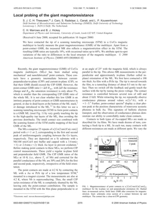
GMR ratio. In Fig. 2, we plot for second-peak contacts the
in-plane MR ratio versus the resistance in saturation, which
is the better defined magnetic state. The open symbols are
points for as-measured curves. The square and triangular
symbols represent two sequences, the point at 57 ⍀ corre-
sponding to the curves of Fig. 1͑a͒. Circular symbols ͑below
25 ⍀͒ represent contacts at different spots. As can be seen,
for RϽ25 ⍀ (diameterϾ10 nm) the ratios are small ͑Ϸ5%͒,
which we attribute to damage in the ML, due to the inden-
tation of the tip. In this range, the coercive field increases
strongly with decreasing resistance, as shown in Fig. 2 ͑left-
hand side axis͒. In the range of 40–80 ⍀, the coercive field
saturates close to the film value ͑45 mT͒. This means that
small indentations by the tip affect the ML only weakly. In
this range, the MR ratios varying between 10%–80% ͑inset
Fig. 2͒. Above 80 ⍀ ͑diameter Ͻ3 nm͒ a strong increase of
the MR ratio sets in, reaching a huge value of 530%.
Globally, contacts to first-peak MLs behave similarly.
They also show a strong increase of the MR ratio above an
onset resistance, even up to values above the maximum
second-peak MR ratio. Among the sequences, the onset re-
sistance varies in the range of 5–60 ⍀. Further, the MR of
these contacts has a saturation field of 200 mT instead of 2 T
for the CIP-control GMR. This may arise from the weaker
coupling of the top Co layer, which is only exchange coupled
to one Co layer, giving a smaller saturation field. However,
we believe that the deviating field scale and the turn up to
large MR ratios with increasing contacts resistance have an
origin extrinsic to the ML, involving the effect of a magnetic
field on the STM.
These contacts are very sensitive to a small displacement
of the tip relative to the film, so that a field-dependent dis-
placement intrinsic to the STM may play a role. To check
this, we measure the MR of contacts to a Au film, which
should be much weaker8
than the effect in Fig. 2. The result-
ing MRs are negative, parabola-like, and, most importantly,
large ͑up to 200%͒. This is exemplified in Fig. 3͑a͒. We
interpret this resistance change as a field-dependent deforma-
tion of parts of the STM, resulting in increasing indentation
of the film by the tip with increasing field, and thus a lower
resistance. This agrees with the increasing tunnel current
with increasing magnetic field measured in tunneling mode
of the STM. We attribute the deformation to magnetostric-
tion of the STM, which is a length change when it becomes
magnetized.9
The STM apparently has parts with residual
magnetism, although its materials are qualified as nonmag-
netic. The Au contact senses the magnetostriction, so that the
ordinate of Figs. 3͑a͒, ͑b͒, and ͑c͒ actually represents mag-
netostriction. Thus, part of the ML contact MR arises from
this displacement effect. The magnetostriction effect due to
the ML itself is negligible.9
The field scale of the overall displacement effect in Fig.
3͑a͒ is comparable to that of the MR of Fig. 1͑b͒ and much
larger than the MR of Fig. 1͑a͒. Thus, the overall displace-
FIG. 2. ͑G͒MR ratio ͑right-hand side axis͒ of ͓Co͑2 nm͒/Cu͑2 nm͔͒25 con-
tacts vs saturation resistance for in-plane field orientation. Open symbols:
measured. Solid symbols: corrected GMR. Corresponding coercive fields
͑left-hand side axis, hour-glass symbols͒ vs saturation resistance. Dashed
line at 45 mT: coercive field of the CIP control GMR. Other lines guide the
eye. Inset: expanded ͑G͒MR for intermediate resistances.
FIG. 3. ͑a͒ MR of a Au contact. ͑b͒ Fine structure in the MR of panel ͑a͒
together with ͑G͒MRs, with scaled resistance values, representative of first-
and second-peak contacts and of the second-peak film. ͑c͒ ␦R/R(HϭHsat)
ϭ͓R(Hϭ0)ϪR(HϭHsat)͔/R(HϭHsat) for Au contacts between 0–3 T
͑parabolic͒ and 0–0.1 T ͑fine structure͒ as a function of R(HϭHsat). Solid
lines: worst-case estimate, used as correction. Dashed lines guide the eye.
2371Appl. Phys. Lett., Vol. 77, No. 15, 9 October 2000 Theeuwen et al.
3. ment can strongly affect the perpendicular GMR, but can
hardly alter the in-plane GMR. More serious for the latter,
however, is the fine-structure present in the curve of Fig. 3͑a͒
close to Hϭ0. This fine structure, plotted in Fig. 3͑b͒ on an
expanded scale, together with scaled MRs representative of
first- and second-peak contacts of intermediate resistance
(40 ⍀ϽRϽ80 ⍀), has a hysteretic maximum at about 55
mT, independent of the contact resistance. The fine structure
corresponds to a displacement of about 0.4 nm, as deduced
from the piezo-voltage change of its tunneling-mode coun-
terpart. Quite incidentally, the field position and shape of the
fine structure are very similar to those of the MR of the
first-peak contacts ͓Fig. 3͑b͔͒. This indicates that the MR of
the first-peak contacts mainly originates from the displace-
ment. However, such a strong similarity does not hold for the
fine structure and the MR of the second-peak contacts, which
are clearly separated ͓Fig. 3͑b͔͒. Rather, the field position of
the second-peak contact is very close to the peak of the CIP
GMR, while its shape is clearly narrower. The latter property
agrees with absence of averaging over many domains in a
point-contact MR. Under the reasonable assumption of a
unique field scale of the displacement effect, part of the
second-peak-contact MR thus is GMR. Apparently, the
second-peak contacts are less sensitive to the displacement,
which is probably related to the different few top layers ͑2
nm Cu/2.4 nm Au instead of 1 nm Cu/3.4 nm Au͒. The
conclusion that part of the MR is GMR agrees with the peak-
position ͑coercivity͒ increase for RϽ25 ⍀ in Fig. 2, which is
absent for Au contacts. The coercivity increase is caused by
destruction of the exchange coupling between neighboring
Co layers due to indentation-induced damage in the ML. For
the two resistances above 80 ⍀, the MR maximum has
shifted to the fine structure of the Au contacts. This means
that the MR is increasingly caused by the displacement ef-
fect.
To correct the MR of the second-peak contacts for the
displacement, a calibration of this effect specific for a
second-peak ML with a 2.4 nm Au cap is needed. Such a
calibration being inaccessible, we use the MR of the Au
contacts for this purpose. Their parabola-like MR and fine
structure, ␦R/R(HϭHsat)ϭ͓R(Hϭ0)ϪR(HϭHsat)͔/R(H
ϭHsat) are plotted as a function of R(HϭHsat) in Fig. 3͑c͒.
Here, Hsat is the saturation field of the ML-contact MR for
the in-plane (0Hsatϭ0.1 T) or perpendicular (0Hsat
ϭ3 T) geometry. ␦R/R(HϭHsat) increases strongly with in-
creasing resistance, which agrees with the intuitively ex-
pected stronger relative change of the contact area per unit
tip displacement for smaller contact areas. This behavior is
similar to that of the MR in Fig. 2, emphasizing the role of
the displacement. To correct the MR ratios of Fig. 2 we use
the worst-case line through the error bars of ␦R/R(H
ϭHsat) ͓Fig. 3͑c͔͒. We add the interpolated ␦R to the satu-
ration resistance of the ML point-contact MR to obtain the
GMR ratio. This correction overestimates the displacement,
since for the same resistance the diameter of a Au contact is
smaller than that of a ML contact.10
GMR curves are ob-
tained by subtracting a Au-contact MR curve with a scaled
amplitude equal to the corresponding ␦R of the worst-case
estimate.
In Fig. 2, the filled symbols denote the GMR ratios. The
ratio is р5% for RϽ25 ⍀, where the signal is mainly GMR.
For the other extreme, RϾ80 ⍀, we find strongly enhanced
ratios of over 200%. Large GMR ratios are very well pos-
sible for the mixed CIP/CPP geometry of the contacts in
combination with a good local magnetic structure. However,
this does not explain the enhancement. Although the en-
hancement may be due to a size effect, e.g., collimation,11
it
is more likely to arise from inadequacy of the correction
procedure for RϾ80 ⍀. In this range, which is somewhat
limited in Fig. 3͑c͒, the resistance is most sensitive to dis-
placement, and the field position of the ML contacts MR has
shifted towards the fine structure of the displacement. For
intermediate resistances 40 ⍀ϽRϽ80 ⍀, on the contrary, a
GMR must remain after correction because of the field-scale
arguments discussed in the context of Fig. 3͑b͒. The two
sequences studied in detail in this range behave differently
͑see inset Fig. 2͒. For one sequence, the GMR ratio takes
values up to 10%, while for the other, it increases with re-
sistance up to 60%. The in-plane GMR curve corresponding
to the 60% point is the solid line in Fig. 1͑a͒, while the solid
line in Fig. 1͑b͒ is the corrected perpendicular GMR with
ratio 90%. The resulting GMR ratio in the intermediate re-
sistance range have to be rather accurate, since the GMR
after correction saturates, as illustrated in Fig. 1.
In conclusion, we have measured the MR of point con-
tacts made by contacting the tip of an STM to a Co/Cu
multilayer. Part of the MR is a magnetostriction effect in the
STM, which dominates for contacts to first-peak MLs, but
leaves a clear GMR for contacts to second-peak MLs. For
the latter, restricting ourselves to sequences of resistances
measured at a spot, we obtain GMR ratios up to 60%, de-
pending on the local quality of the ML.
1
M. V. Tsoi, A. G. M. Jansen, and J. Bass, J. Appl. Phys. 81, 5530 ͑1997͒.
2
K. P. Wellock, S. J. C. H. Theeuwen, J. Caro, N. N. Gribov, R. P. van
Gorkom, S. Radelaar, F. D. Tichelaar, B. J. Hickey, and C. H. Marrows,
Phys. Rev. B 60, 10291 ͑1999͒.
3
C. H. Marrows, N. Wiser, B. J. Hickey, T. P. A. Hase, and B. K. Tanner,
J. Phys.: Condens. Matter 11, 81 ͑1999͒.
4
J. Wildoe¨r, thesis, TU Delft, 1996.
5
A. I. Yanson, G. R. Bollinger, H. E. van den Brom, N. Agrait, and J. M.
van Ruitenbeek, Nature ͑London͒ 395, 783 ͑1998͒.
6
P. A. M. Holweg, J. Caro, A. H. Verbruggen, and S. Radelaar, Phys. Rev.
B 45, 9311 ͑1992͒.
7
N. Garcı´a, M. Mun˜oz, and Y.-W. Zhao, Phys. Rev. Lett. 82, 2923 ͑1999͒.
8
P. A. M. Holweg, J. A. Kokkedee, J. Caro, A. H. Verbruggen, S. Radelaar,
A. G. M. Jansen, and P. Wyder, Phys. Rev. Lett. 67, 2549 ͑1991͒.
9
See e.g., R. M. Bozorth in Ferromagnetism ͑Van Nostrand, Toronto,
1951͒, who also reports that the magnetostriction of Co is Ϸ10Ϫ5
. For the
50 nm thick Co in the ML the thickness change thus is 0.5ϫ10Ϫ3
nm.
10
We estimate the contact diameter from the resistance R using Wexler’s
formula ͓G. Wexler, Proc. Phys. Soc. 89, 927 ͑1966͔͒ dϭ(tipϩx)/4R
ϩ1/R•ͱ(tipϩx)2
/2ϩ16/3R(l)x with tip the resistivity of the tip and
x that of the Au or ML film and l the mean free path. lϷ1 f⍀m2
͓J.
Bass, Landolt Bo¨rnstein New Series, ͑Springer, Berlin, 1982͒, vol. III/
15a͔, and ML /AuϷ20, so that dML /dAuϭ1–20.
11
Collimation is a narrowing of the angular injection distribution, a known
effect in ballistic constrictions in GaAs ͓C. W. J. Beenakker and H. van
Houten, Solid State Phys. 44, 1 ͑1991͔͒. For neck-shaped ML constric-
tions collimation not only leads to a stronger CPP-like current, but also to
a higher probability of backscattering through the orifice for specular scat-
tering at the interfaces. A collimated current along specific crystallo-
graphic directions leads to enhanced reflection probabilities, and thus, an
enhanced GMR.
2372 Appl. Phys. Lett., Vol. 77, No. 15, 9 October 2000 Theeuwen et al.