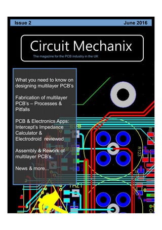
1. Circuit Mechanix
What you need to know on
designing multilayer PCB’s
Fabrication of multilayer
PCB’s – Processes &
Pitfalls
PCB & Electronics Apps:
Intercept’s Impedance
Calculator &
Electrodroid reviewed
Assembly & Rework of
multilayer PCB’s.
News & more...
Issue 2 June 2016
The magazine for the PCB industry in the UK
2. Circuit Mechanix
Contents
Article:
Multilayer PCB’s - What you need to know P. 3
Review:
Electronics Apps - Electrodroid P.6
Intercepts Impedance Calculator Tool P. 10
Industry News P. 12
Article:
Processes and pitfalls of Multilayer
fabrication every designer needs to know. P.8
Article:
Assembly and re-work of multilayer PCB’s P. 13
Page 1 Circuit Mechanix – June 2016
Circuit Mechanix
June 2016 – Issue 1
The PCB magazine for
the UK printed circuit
industry. Contents:
3. Mechanix Musings
If you’re reading this then we made it to the second issue of Circuit Mechanix. What you
the reader may also notice is that this issue isn’t focussing on flex as stated in the first
issue but on multilayer boards, this is also true – I changed my mind. As the great Captain
Picard might say “That’s Captain’s prerogative”. I felt that dealing with many of the
issues facing us with multilayer boards was a place to start that applies to more engineer –
it’s also maybe a nice surprise!
Multilayer boards are a fact of life in electronics now and when designing them there are
many facts and possibilities to consider, sometimes with more than one answer. Knowing
what all these are and the consequences is key to getting it right. I hope this issue goes
some way to helping with this.
As the reader base for Circuit Mechanix increases I would like to hear from you, the
issues you have, the problems you can or can’t solve as this will give me the feedback I
need on the real problems you as engineers face so I can direct the content at these areas
and who knows – maybe we can all learn something? If you’re interested use the email to
get in contact.
Circuit Mechanix is aimed at being a useful, practical source of information for engineers
and technicians working in the PCB industry. If you want more information, feel like you
can contribute in some way or if you’re a company that wants to see your name in Circuit
Mechanix then send an email to: circuitmechanix@gmail.com.
Page 2 Circuit Mechanix – June 2016
Circuit Mechanix
4. Todays world of high speed, high pin
count high power density electronics
means designing multilayer PCB’s is
almost essential for any design.
Multilayer boards enable a designer to
be able to integrate controlled
impedances for high speed and RF
circuits with power circuits easily and
efficiently without taking up large
amounts of space and eliminating the
need to use jumper links to make
connections.
But as engineer’s knowing how our
multilayer boards are built is key to
ensuring design success. Knowing the
materials that will be used at the
fabricator, so the right cores and pre-
pregs are used is are particularly
important for impedance control.
Allowing enough time and effort to work
out the number of layers required and
their stackup will be time well spent.
While this can be changed during the
design, it may mean that other design
elements will be affected and time
wasted in re- design to account for this.
So it needs to be planned well.
So, how does a PCB Designer work all
of this out?
Layers – Deciding on grounding and
power strategies will give us the best
guide on the layers we need. Ask these
questions:
1) How many ground planes needed?
Are there different ground on
different planes or are they split?
2) How many power rails are there? Is
a layer being allowed for each
power rail or are we splitting them?
Will they be split into area above
each other to stop ground bounce?
3) What and how many signals are
there to route? Will there need to be
signals routed on inner layers and
will these need to be protected from
the power layers?
4) Just a plain through hole board or
are blind / buried vias being
employed?
Page 3 Circuit Mechanix – June 2016
Designing Multilayer PCB’s – What you need to know
5. Page 4 Circuit Mechanix – June 2016
Designing Multilayer PCB’s – What you need to know
Stackups:
The stackup shown on the left is typical of a
simple 4 layer PCB. The signal layers are
indicated with broken conductors, the ground
or power planes are shown as solid
conductors. The thicker PCB core is
sandwiched between the thinner prepregs.
4 Layer PCB Stackup:
Plane Arrangement:
The plane arrangement shown here depicts a
number of planes one on top of the other on
different layers. They will be a mix of power
and ground nets. This is an acceptable way to
arrange power and ground planes.
However in order to minimise ground bounce in
a circuit, the power and ground planes could
follow the same shaped profile on each layer,
this reduces the coupling between power and
ground. An example profile of this is shown – it
could be any shape, but would follow the same
profile on each layer for power and ground.
Note:
For ground planes it’s generally accepted that
splitting planes creates signal integrity ‘gaps’.
While sometimes it’s unavoidable to split a
plane, if possible it’s best avoided.
7. When I got my first Android phone it
was suggested I look up an app called
Electrodroid. After installing it, I was
instantly impressed. Electrodroid is only
available on Android and is the app to
have for any and every kind of
electronics engineer and technician. As
shown above there are four tabs to
choose a vast array of useful
information that’s available on the go
from your device.
Calculators - has a range of different
calculators to help with everything from
resistor codes to filters and PCB trace
width calculation. All of this in one
place.
The next tab has a whole list of
Pin-Outs – think of a connector used in
everyday electronics – it’s probably
here. On top of this are pin outs for
Raspberry Pi, Arduino’s and
Beaglebone boards also.
The next tab is a Resource table for
component selection, wiring size tables
and chip databases.
The amount information available to the
Electrodroid user is massive and it’s
accurate, quality information that can be
relied on.
Electrodroid is also expandable, with a
number of Plugins that are designed to
work with it.
.
Page 6 Circuit Mechanix – June 2016
Review: Electronics Apps - Electrodroid
9. Multilayer PCB’s are layers of copper
area’s etched to their patters to form a
single circuit that all connects together,
just like in the design. Easy eh?
We wish! When we scratch away at the
process behind the design we lean that
maybe all is not what we might think.
Defining the stackup before routing
even starts is essential. This is because
the stackup will define where the
designer can route, where ground and
power planes are located and where
any controlled impedances will be
routed too. Time spent at this stage isn’t
wasted, it’s well spent as this can save
time later in tearing up chunks of design
work and starting again.
Being realistic about the number of
layers will also be beneficial at this
stage, this means balancing (as always)
cost against technical performance.
Discussing the requirements with the
fabricator at this stage means that this
stage of the build is designed and we
don’t have to mess with it later.
Copper balance is a factor to be
considered that few outside PCB design
and fabrication know about – yet with
multilayer boards it can have a
profound effect. The effect of bad
copper balance is a warped board and
is caused if a board is designed with
some areas of highly dense copper
features where on other parts it’s less
dense.
Planes which over lap across the layers
is often enough to cure this, either that
or filling in between routed areas with
ground pour. If doing this, make sure
that no creepage distances, or other
circuit features are compromised.
Drill holes and vias seem like a simple
affair – on the whole they are. But when
a plated hole is defined in your design –
is this the size of the hole drilled or after
plating? Normally this isn’t an issue, but
if using custom assemblies with fine
wires, problems can arise where the
wire doesn’t fit in the hole as expected.
Continued4
Page 8 Circuit Mechanix – June 2016
Featured Article: Processes and pitfalls of
multilayer fabrication every designer needs to
know
11. It’s not greatly known that Intercept,
the company behind the Pantheon
PCB / Hybrid design software had
released a controlled impedance
calculator for mobile and tablet.
The app is available for either
Android or Apple platforms and the
first impression is a clean,
uncluttered look. There are seven
basic options and each one brings up
the required variables. The power of
this app is in it’s ease of use, the
user prompted for the required
values.
Where there is a calculator next to a
value is where the user can leave the
value blank. Input the other
variables, press on the one
remaining (which is shown in red)
and there you go – your required
value appears.
After diving into the other functions in
the app the operation is much the
same, the amount of variables
change depending on what’s being
calculated, but the user only needs
to have a basic understanding to
operate this and get a sensible
answer.
Review: Intercept Impedance Calculator
Page 10 Circuit Mechanix – June 2016
13. Options are now availabl
Circuit Mechanix
Page 12 Circuit Mechanix – June 2016
Industry News:
Anglia Circuits have recently invested in a
Bacher auto alignment printing machine.
Improving their registration capability
significantly.
www.angliacircuits.com
Sionics
Improved feedback options are now
available on library parts.
www.snapeda.com
Sionics are working with to achieve
ISO13485 approval over the next few
months with plans to expand their service
offering around this later.
www.sionics.co.uk
14. Multilayer PCB’s are being used in
almost every electronic device that can
be thought of. This is especially true in
higher density electronic devices where
components are crammed into the
smallest space possible. The reason for
this? It enables the engineer to track
out the circuit in a tight area while
providing functionality like impedance
control.
Multilayer PCB’s also provide excellent
thermal conductivity to be able to get
heat away from components without the
need of heat sinks.
This kind of approach is bound to have
an effect on the way PCB’s are
assembled and re-worked. Soldering
parts down to a board can be hard
enough, but getting them off again
without damaging the board can be
much harder.
Assembly and Reflow:
Applying the paste and placing
components onto a multilayer PCB
happens in the same way as a single
sided PCB. The problems come during
reflow.
Imagine the PCB that’s being worked
on now going through a big heater and
being warmed up to a thermal profile
like this one:
The area’s of copper that are larger are
going to sap the heat away faster and
will therefore take longer to heat up
than the area’s where there is little
excess copper. So all the different parts
of the circuit are warming up at different
rates. This could potentially lead to
solder re-flow taking place at different
times. This could lead to components
tombstoning, reflow not taking place
underneath IC’s with power pads and
dry joints. Basically – a PCB engineer’s
nightmare.
Continued on next page4
Page 13 Circuit Mechanix – June 2016
Article: Assembly and Rework of Multilayer PCB’s
15. Assembly and Rework of Multilayer
PCB’s continued4
Compensating for this is usually done
by increasing the dwell time (referred to
as the soaking zone in the chart) the
board is subjected to. This ensures that
every part of the PCB is at the right
temperature for the fluxes to start
working and will reach the desired peak
temperature, with all the solder joints
forming as they should.
Another reflow process used is the
vapour phase reflow process, where
heat transfer liquid gasses are used to
heat every part of the PCB and the
components uniformly. The issue with
the vapour phase process is that it’s not
a mass production process and is often
slower than using IR reflow ovens. The
vapour phase process can damage
some sensitive components, so make
sure evert component is suitable.
So now the components are down on
the board – what about re-work and
repair?
Rework & Repair:
In order to carry our PCB repairs, two
things are needed:
1) The right tools
2) A well trained / experienced operator
A good soldering iron like a Metcal
system with interchangeable tips and a
talon system are essential to carry out
good re-work. The heat is used
efficiently and the tips transfer the heat
well. A good rule of thumb is to use the
largest tip possible, particularly in the
removal process. A talon system allows
the operator to use different sized tips
to ‘pinch’ the component on each side
and remove very easily with no PCB
damage incurred.
PCB damage during component
removal is common, but with modern
small pad sizes, not as easy to repair
as ten or more years ago.
Continued on next page4
Page 14 Circuit Mechanix – June 2016
Interested in seeing your company name in here, or
doing something you want to tell everyone about?
Email circuitmechanix@gmail.com for more
information.
17. Circuit Mechanix
Next issue out in September 2016 - What’s
going to be in it?
Articles:
Miniaturisation – The swings and roundabouts
of how to shrink your circuits – and how to deal
with them.
Review:
Choosing your PCB design tool
And more4
Page 16 Circuit Mechanix – June 2016
Next Issue: