The document is the first issue of Circuit Mechanix magazine focusing on the printed circuit board industry in the UK. It includes articles on the assembly process, what designers should provide to fabricators after design, and what fabricators do with design data. It also reviews the ZofzPCB gerber verification tool and provides industry news briefs.
Pcb designing and working explanation and full theory
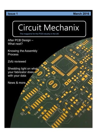
Circuit Mechanix Mar 2016
1. Circuit Mechanix
After PCB Design –
What next?
Knowing the Assembly
Process
Zofz reviewed
Shedding light on what
your fabricator does
with your data
News & more...
Issue 1 March 2016
The magazine for the PCB industry in the UK
2. Circuit Mechanix
Contents
Article:
What should happen after PCB Design? P. 3
Review:
ZofzPCB P. 4
Industry News P. 6
Article:
Knowing your PCB Assembly
Process P. 7
Article:
Shining the what your
PCB Fabricator with your data. P. 9
Page 1 Circuit Mechanix – March 2016
Circuit Mechanix
March 2016 – Issue 1
The PCB magazine for
the UK printed circuit
industry. Contents:
3. Mechanix Musings
Welcome to Circuit Mechanix, the first issue of a magazine focussing on the Printed
Circuit industry in the UK. This project has been rattling around in my brain for some
time and it was at the beginning of this year that I decided to just go for it and make it
happen.
Circuit Mechanix is aimed at being a useful, practical source of information for engineers
and technicians working in the PCB industry. There will hopefully be an issue every
quarter, which will hopefully generate interest from other individuals and companies. If
you want more information, feel like you can contribute in some way or if you’re a
company that wants to see your name in Circuit Mechanix then send an email to:
circuitmechanix@gmail.com.
Now that the introductions are out of the way, let’s get down to business. What’s the first
issue about? This first issue is about that tedious but key part of the process between
design and manufacture. It’s an area that’s rarely covered and yet can be the source of so
much pain. The articles in this first issue of Circuit Mechanix are should help guide the
reader the obstacles by pointing out what can go wrong and how to overcome .
On a more light hearted note, there’s the introduction of Numptyz – a cartoon strip
looking at the ironic and satirical side of the workplace. It’s an old format, but with new
characters with twist of contorted ‘common’ sense.
Page 2 Circuit Mechanix – March 2016
Circuit Mechanix
5. PCB’s are becoming more complex and
a critical part of almost all modern
systems. Design tools have a huge
array of features to get the design how
the designer wants it. Verifying
manufacturing information against the
design is critical as mistakes can occur
in the translation on rare occasions. It’s
surprising that EDA vendors haven’t
addressed this gap in the process.
Recently I was introduced to ZofzPCB –
a gerber viewing and verification tool
that I hadn’t heard of before.
Unlike other 2D gerber viewers,
ZofzPCB lets the designer see the
PCB’s manufacturing data in a 3D
format, it enables the designer to split
the board apart and view the inner
layers and how they’re connected.
More importantly, by importing an IPC-
D-356A netlist from the design into
ZofzPCB an error check of the gerber
files can be carried out. While gerber
errors from design systems are rare,
they do happen and the cost in lost time
and materials is expensive to say the
least.
Page 4 Circuit Mechanix – March 2016
Review: ZofzPCB – Enhancing the design Process
7. Circuit Mechanix
Page 6 Circuit Mechanix – March 2016
Industry News:
Anglia Circuits have recently invested in a
Bacher auto alignment printing machine.
Improving their registration capability
significantly.
Epoxy filling of via is now available for PCB’s
in prototype quantities.
www.angliacircuits.com
Sionics
SnapEDA have just launched an
experimental plugin for Eagle users, allowing
easy access to SnapEDA from within the
Eagle PCB design tool
www.snapeda.com
Sionics are working towards the ISO13485
approval for Medical Devices. A positive
outcome is expected within a few months.
www.sionics.co.uk
8. It’s always a time of mixed emotions
when a new batch of PCB’s arrives on
your desk, fresh from the subcontractor.
Excitement of testing the design that’s
had time, blood, sweat and tears put
into it. Hoping they work after all the
time and money that’s been spent on
them. Knowing the assembly process
can give a designer or engineer greater
confidence in the finished boards.
Different aspects that can be
considered are:
Paste Screens – How the paste
apertures are defined in a design can
be important to the assembler. Find out
how the paste apertures are used in the
solder screens. What often happens is
the paste aperture in the gerber files for
a PCB will be a 1:1 representation of
the pad and this is used by a separate
stencil fabricator to make the paste
screens. Check what a subcontractor
does though, an incorrect assumption
could lead to the incorrect quantity of
paste being applied.
Handling – How well setup is your
subcontractor to handle ESD (Electro
Static Discharge) and moisture
sensitive components? Are there
equipment and controls in place to
handle them? Controlling static is often
regarded as unnecessary, however it is
a real risk to components. The same
applies to moisture sensitivity, which
components are rated as moisture
sensitive in the design? What impact
will this have?
Reflow – What reflow process does
your subcontractor use as standard?
Normally this doesn’t matter, however
some components can be damaged by
vapour phase reflow processes. Not
only is a good knowledge of the
assembly process required but an
intimate search of component
datasheets is sometimes necessary.
Checking individual assembly
requirements of the components is
often hard as the information that’s
important is buried deep in the
datasheet on page 12 in small text
which isn’t highlighted.
Continued…
Page 7 Circuit Mechanix – March 2016
Article: Knowing your PCB assembly process
10. After the design process is complete
and the fabrication data, is generated
and checked (I’m sure everyone
reading this checks their data before
giving it to the fabricator) it’s sent to the
fabricator and after a few days some
PCB’s arrive back, just like the PCB’s
that were designed. It’s simple right?
But what has the fabricator done to /
with your data?
Have you asked for your fabricator to
check the gerbers against a netlist?
Is the panel data reviewed before
production commences?
Why is it even important? Like all these
things, it’s impossible to know until the
question is asked!
The next time PCB data is sent to your
fabrication company why not ask them
a few things:
Ask them to make a list of the changes
they make. With the best will in the
world the design rules the design is
checked against are often not set up to
the manufacturers constraints. This kind
of information will help you understand
what they need better.
Most of the time PCB’s are supplied in
panels, how they are aligned can cause
issues with your product (where the
breakouts are for example) or possibly
the manufacturing process. Having a
review on the panel data and possibly
having the assembler look at it, (if the
design complexity demands it) can help
smooth out the assembly process.
If you’ve provided your fabricator with a
netlist to check the gerbers against,
have you checked to make sure they
can read it?
Is your fabricator carrying out this
check?
Continued on next page…
Page 9 Circuit Mechanix – March 2016
Article: Shining the light on what your PCB Fabricator
does with your data
12. Circuit Mechanix
Next issue out in June 2016 - What’s going to be
in it?
Articles:
Designing flex and flex rigid PCB’s - The
practical point of view.
Presenting data to your fabricator.
Review:
Mobile apps for engineers and technicians.
And more…
Page 11 Circuit Mechanix – March 2016
Next Issue: