What are The key considerations in The Design of Probe Cards For Semiconductor Testing in California's technology industry
•
0 likes•3 views

What are The key considerations in The Design of Probe Cards For Semiconductor Testing in California's technology industry

Recommended
Recommended
More Related Content
Similar to What are The key considerations in The Design of Probe Cards For Semiconductor Testing in California's technology industry
Similar to What are The key considerations in The Design of Probe Cards For Semiconductor Testing in California's technology industry (20)
More from Semi Probes Inc
More from Semi Probes Inc (20)
Recently uploaded
Recently uploaded (20)
What are The key considerations in The Design of Probe Cards For Semiconductor Testing in California's technology industry
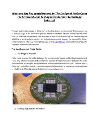
- 1. What are The key considerations in The Design of Probe Cards For Semiconductor Testing in California's technology industry? The ever-evolving landscape of California's technology sector, semiconductor testing stands out as a crucial stage in the production process. At the heart of this intricate process lies the probe card – a small yet indispensable tool that plays a pivotal role in ensuring the functionality and reliability of semiconductor devices. As technology advances, so does the demand for higher performance and efficiency, making the design of Probe Card Design an area of intense focus for engineers and manufacturers alike. The Significance of Probe Cards: 1. The Bridge to Precision Probe cards serve as the bridge between the semiconductor device and the testing equipment. These tiny, often underestimated components facilitate the communication between the tester and the device, allowing for a comprehensive evaluation of the semiconductor's functionality. As California's technology industry continues to push the boundaries of innovation, the importance of reliable and efficient probe cards becomes increasingly evident. 2. Enabling High-Volume Production
- 2. In the fast-paced world of semiconductor manufacturing, efficiency is key. Probes and cards are essential for enabling high-volume production by rapidly testing multiple devices simultaneously. This not only reduces manufacturing time but also ensures that only fully functional semiconductors move forward in the production pipeline. This emphasis on efficiency aligns with California's tech ethos, where speed and precision are paramount. Key Considerations in Probe Card Design: • Contact Technology The heart of any probe card is its contact technology. This involves the design of the microscopic needles or pins that make contact with the semiconductor device for testing. In California's tech industry, where advancements are rapid, the choice of contact material is crucial. High-quality materials with excellent conductivity are preferred to ensure reliable and accurate testing. Additionally, considerations for wear resistance and durability become vital to withstand the rigors of high-volume testing. • Pitch and Density As semiconductor devices become smaller and more complex, the pitch – the distance between individual probes – becomes a critical factor. California's technology industry, known for pushing the limits of miniaturization, demands probe cards with high pitch and density capabilities. Engineers must strike a delicate balance between compact designs to accommodate smaller devices and the need for a sufficient number of probes to ensure comprehensive testing. • Temperature Management Semiconductor testing often involves exposing devices to varying temperatures. Probe cards must be designed to handle these temperature fluctuations without compromising performance. In the temperate climate of California, where temperature differentials can be significant, ensuring that probe cards remain reliable across a range of conditions is paramount. Thermal management solutions, such as efficient heat dissipation mechanisms, are integral to the design process. • Signal Integrity In the quest for higher performance, maintaining signal integrity is a critical consideration. Probes and cards must be designed to minimize signal loss and distortion during testing. California's tech industry, known for its cutting-edge applications in fields like artificial intelligence and autonomous vehicles, requires probe cards that can handle high-frequency signals without compromising accuracy. Advanced signal processing technologies are employed to ensure optimal performance.
- 3. • Adaptability and Customization The diverse landscape of California's tech industry means that semiconductor devices come in various shapes, sizes, and configurations. Probes and cards must be adaptable and customizable to accommodate this diversity. Modular designs that allow for easy configuration changes and adjustments to different semiconductor layouts are essential. The ability to quickly adapt to evolving technological requirements is a hallmark of the state's tech ecosystem. • Reliability and Lifecycle Considerations Reliability is non-negotiable in the semiconductor testing realm. Probes and cards must undergo rigorous testing to ensure they can withstand the demands of high-volume production. California's tech industry, characterized by its commitment to sustainability, also emphasizes the importance of extending the lifecycle of components. Probe card designs that incorporate robust materials and construction contribute to reducing electronic waste and align with the state's environmental goals. Challenges and Innovations in Probe Card Design: • Overcoming Miniaturization Challenges As semiconductor devices continue to shrink in size, probe card design faces the challenge of miniaturization. Engineers in California's tech industry are at the forefront of developing innovative solutions to overcome this challenge. Advanced manufacturing techniques, such as microfabrication and precision machining, are employed to create probes and cards with smaller form factors without compromising performance. • Integration of Advanced Technologies The integration of advanced technologies, such as artificial intelligence and machine learning, is another frontier in probe card design. These technologies enhance the efficiency of semiconductor testing by optimizing test patterns, predicting potential failures, and improving overall testing accuracy. California's tech industry, renowned for its emphasis on innovation, is driving the adoption of these technologies in probe card design to stay ahead in the global semiconductor market. Future Trends in Probe Card Design: • 5G and Beyond The rollout of 5G technology is transforming the landscape of connectivity, and probes and cards play a crucial role in ensuring the reliability of 5G semiconductor devices. As California's tech
- 4. industry continues to lead the way in 5G innovation, probe card designs will evolve to meet the unique testing requirements of high-frequency and high-speed communication technologies. • AI-Driven Testing The integration of artificial intelligence into semiconductor testing is set to become more pervasive. AI-driven testing not only improves testing accuracy but also enables real-time adjustments based on dynamic testing conditions. California's tech industry, with its focus on AI applications, is expected to drive the adoption of AI-driven probe card designs. • Sustainability Initiatives In alignment with California's commitment to sustainability, future probe card designs are likely to incorporate eco-friendly materials and manufacturing processes. Reducing the environmental impact of electronic waste is a priority, and probe card manufacturers will strive to create designs that are both high-performing and environmentally responsible. Conclusion: The design of Probe Card Manufacturers for semiconductor testing in California's technology industry is a fascinating intersection of precision engineering, innovation, and adaptability. As the state continues to be a global technology powerhouse, the evolution of probe card designs will undoubtedly play a crucial role in shaping the future of semiconductor manufacturing. With a focus on contact technology, pitch and density, temperature management, signal integrity, adaptability, and reliability, California's engineers are poised to lead the way in developing probe cards that meet the ever-growing demands of the tech industry. As we look to the future, the integration of advanced technologies and a commitment to sustainability will further define the landscape of probe card design, ensuring that California remains at the forefront of semiconductor testing innovation.