What are The Latest Trends and Innovations in Probe Card Design Being Developed in California
•
0 likes•3 views

What are The Latest Trends and Innovations in Probe Card Design Being Developed in California

Recommended
Recommended
More Related Content
Similar to What are The Latest Trends and Innovations in Probe Card Design Being Developed in California
Similar to What are The Latest Trends and Innovations in Probe Card Design Being Developed in California (20)
More from Semi Probes Inc
More from Semi Probes Inc (20)
Recently uploaded
Recently uploaded (20)
What are The Latest Trends and Innovations in Probe Card Design Being Developed in California
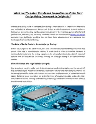
- 1. What are The Latest Trends and Innovations in Probe Card Design Being Developed in California? In the ever-evolving realm of semiconductor testing, California stands as a hotbed for innovation and technological advancements. Probe card design, a critical component in semiconductor testing, has been witnessing rapid developments, driven by the relentless pursuit of enhanced performance, efficiency, and reliability. The latest trends and innovations in Probe Card Design emerging from California, shedding light on how these advancements are reshaping the landscape of semiconductor testing. The Role of Probe Cards in Semiconductor Testing: Before we plunge into the latest trends, let's take a moment to understand the pivotal role that probe cards play in semiconductor testing. A probe card is a crucial interface between a semiconductor wafer and the testing equipment. Its primary function is to establish electrical contact with the circuitry on the wafer, allowing for thorough testing of the semiconductor devices. Miniaturization and High-Density Designs: One prominent trend in probe card design revolves around miniaturization and the pursuit of high-density designs. As semiconductor devices become smaller and more complex, there is an increasing demand for probe cards that can accommodate a higher number of probes in a limited space. California-based innovators are at the forefront of developing probe cards with ultra- compact form factors, allowing for the testing of densely packed semiconductor wafers without compromising on precision.
- 2. Advanced Materials and Manufacturing Techniques: In the quest for improved performance, probe card designers are exploring advanced materials and manufacturing techniques. Materials with superior electrical and thermal properties are being incorporated into probe card designs to enhance conductivity and dissipate heat effectively. Moreover, innovative manufacturing processes, such as 3D printing and advanced lithography, are being harnessed to create intricate and precise probe card structures, pushing the boundaries of what was once deemed possible. Multi-Die Testing Capabilities: With the rise of multi-die semiconductor devices, there is a growing need for probe cards that can efficiently test multiple dies simultaneously. California-based companies are spearheading the development of probe cards with multi-die testing capabilities, allowing semiconductor manufacturers to streamline their testing processes and improve overall efficiency. This trend is particularly significant as it addresses the challenges posed by the increasing complexity of semiconductor designs. Adoption of Artificial Intelligence in Testing Algorithms: In an era dominated by artificial intelligence (AI), it comes as no surprise that probe card designers in California are integrating AI into testing algorithms. AI-driven testing algorithms can adapt to the unique characteristics of each semiconductor device, optimizing the testing process and improving the accuracy of results. This not only enhances the efficiency of semiconductor testing but also contributes to the development of more reliable and robust electronic components. Enhanced Probing Technologies: The core functionality of a probe card lies in its ability to establish electrical contact with the semiconductor wafer. In California's tech laboratories, there is a strong focus on enhancing probing technologies. From innovative contact materials to advanced probe tip designs, these developments aim to improve signal integrity, reduce contact resistance, and ensure consistent and reliable electrical connections during testing. Integration of Sensing and Monitoring Systems: To address the dynamic nature of semiconductor testing, probe card designers are increasingly integrating sensing and monitoring systems into their designs. Real-time monitoring of temperature, contact force, and other relevant parameters allows for proactive adjustments during testing, ensuring optimal conditions and preventing potential issues that could
- 3. compromise test results. This trend reflects the commitment to precision and reliability in semiconductor testing processes. Environmental Sustainability in Probe Card Design: As the global focus on environmental sustainability intensifies, California-based innovators are incorporating eco-friendly practices into Probe Card Design. This includes the use of recyclable materials, energy-efficient manufacturing processes, and the development of probe cards with extended lifecycle durability. The push towards sustainability not only aligns with global environmental goals but also contributes to creating a more responsible and resilient semiconductor industry. Conclusion: California's status as a technological powerhouse is evident in the groundbreaking developments in probe card design. From miniaturization and high-density designs to the integration of AI and sustainability practices, the trends emerging from this tech hub are shaping the future of semiconductor testing. As we look ahead, it's clear that the synergy of innovation, expertise, and a relentless pursuit of excellence will continue to propel probe card design into new frontiers, unlocking possibilities that will redefine the capabilities of electronic devices for years to come.