The Art of Probe Card Design in California A Journey into Silicon Valley's Hidden Gems
•
0 likes•2 views

The Art of Probe Card Design in California A Journey into Silicon Valley's Hidden Gems

Recommended
Recommended
More Related Content
Similar to The Art of Probe Card Design in California A Journey into Silicon Valley's Hidden Gems
Similar to The Art of Probe Card Design in California A Journey into Silicon Valley's Hidden Gems (20)
More from Semi Probes Inc
More from Semi Probes Inc (20)
Recently uploaded
Recently uploaded (20)
The Art of Probe Card Design in California A Journey into Silicon Valley's Hidden Gems
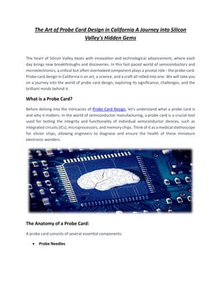
- 1. The Art of Probe Card Design in California A Journey into Silicon Valley's Hidden Gems The heart of Silicon Valley beats with innovation and technological advancement, where each day brings new breakthroughs and discoveries. In this fast-paced world of semiconductors and microelectronics, a critical but often overlooked component plays a pivotal role - the probe card. Probe card design in California is an art, a science, and a craft all rolled into one. We will take you on a journey into the world of probe card design, exploring its significance, challenges, and the brilliant minds behind it. What is a Probe Card? Before delving into the intricacies of Probe Card Design, let's understand what a probe card is and why it matters. In the world of semiconductor manufacturing, a probe card is a crucial tool used for testing the integrity and functionality of individual semiconductor devices, such as integrated circuits (ICs), microprocessors, and memory chips. Think of it as a medical stethoscope for silicon chips, allowing engineers to diagnose and ensure the health of these miniature electronic wonders. The Anatomy of a Probe Card: A probe card consists of several essential components: • Probe Needles
- 2. At the heart of every probe card are the probe needles, which make direct contact with the semiconductor device being tested. These needles must be incredibly precise, both in their size and alignment, to ensure accurate testing without damaging the delicate chips. • Ceramic Substrate The ceramic substrate serves as the foundation of the probe card, providing stability and electrical connectivity. It acts as a bridge between the probe needles and the testing equipment. • Wiring and Connectors Wiring and connectors are responsible for transmitting electrical signals between the probe needles and the testing equipment. These components must be meticulously designed to minimize signal loss and interference. • Alignment Mechanism An alignment mechanism ensures that the probe needles make accurate and consistent contact with the semiconductor device. Precision is paramount here, as even the slightest misalignment can lead to erroneous test results. The Significance of Probe Card Design: • Quality Assurance in Semiconductor Manufacturing In the semiconductor industry, where a single defective chip can lead to massive losses, the role of the probe card in quality assurance cannot be overstated. Before a semiconductor device can make its way into consumer electronics, automobiles, or industrial machinery, it must undergo rigorous testing to identify and rectify any manufacturing defects. • Time-to-Market and Cost Efficiency Time-to-market is a critical factor in the highly competitive world of electronics. Faster testing and validation of semiconductor devices can significantly accelerate product development cycles. A well-designed probe card can help streamline this process, saving both time and resources. • Ensuring Reliability Reliability is paramount in industries that rely on semiconductor devices for mission-critical applications. Probe card design plays a crucial role in ensuring that these devices meet strict reliability standards, from aerospace and defense to healthcare and telecommunications. The Art of California Probe Card Design:
- 3. • The Hub of Semiconductor Innovation When you think of California, the first thing that likely comes to mind is Silicon Valley, the epicenter of global tech innovation. Home to giants like Apple, Google, and Tesla, this region is also a breeding ground for cutting-edge semiconductor technology. It's no surprise that probe and card design in California is at the forefront of technological advancement. • The Marriage of Art and Engineering Probe card design is not merely a technical endeavor; it's an art form. In California, where creativity and innovation are prized above all else, the marriage of art and engineering is a defining feature of probe card design. Engineers and designers in the region don't just create functional probe cards; they craft them with an eye for precision and elegance. • Collaborative Ecosystem The success of California's probe card design industry can be attributed in part to the collaborative ecosystem that thrives in the region. Companies, research institutions, and startups work hand in hand to push the boundaries of what probe cards can achieve. This collaborative spirit fosters an environment where ideas are shared freely, leading to rapid innovation. The Challenges of Probe Card Design: • Miniaturization As semiconductor devices continue to shrink in size, the challenges of probe card design become more daunting. Probe needles must now make contact with microscopic features, requiring engineering feats of unparalleled precision. • Signal Integrity Maintaining signal integrity in the face of shrinking dimensions and increasing data rates is a constant battle. Designing probe cards that can reliably transmit high-frequency signals without interference is a Herculean task. • Material Selection The choice of materials for probe card components is critical. Engineers in California constantly explore new materials that offer the right balance of electrical conductivity, durability, and thermal properties. • Cost-Efficiency
- 4. While pushing the boundaries of technology is essential, it's equally important to do so cost- effectively. Probe card designers in California must strike a delicate balance between innovation and affordability. Innovations in California Probe Card Design: • 3D Printing One of the most exciting innovations in probe card and design in California is the adoption of 3D printing technology. This revolutionary approach allows for the rapid prototyping of probe card components with unmatched precision. It also enables the creation of intricate designs that were once thought impossible. • Machine Learning and AI California's tech-savvy engineers are harnessing the power of machine learning and artificial intelligence to optimize probe card design. These technologies are used to predict potential issues, improve alignment, and enhance signal processing, ultimately leading to more efficient and reliable probe cards. • Nanotechnology Nanotechnology is another area where California's probe card designers are making strides. By leveraging nanoscale materials and structures, they can achieve unprecedented levels of precision and performance in probe cards. The Future of Probe Card Design in California: • Quantum Computing As the semiconductor industry continues to push the boundaries of computing, probe card design in California is gearing up for the era of quantum computing. These revolutionary machines require probe cards that can operate at extremely low temperatures and interact with qubits, the fundamental units of quantum information. • Sustainability In California, where environmental consciousness is a way of life, there is a growing emphasis on sustainable probe cards and design. Engineers are exploring eco-friendly materials and manufacturing processes to reduce the environmental footprint of probe card production. • Global Impact
- 5. The innovations in probe card design coming out of California are not confined to the state's borders. They have a global impact, shaping the future of the Semiconductor Industry worldwide. California's probe card and designers are influencing the development of electronics that touch every aspect of modern life, from smartphones to autonomous vehicles.