Exploring The Intricacies of Probe Card Manufacturing
•
0 likes•3 views

Exploring The Intricacies of Probe Card Manufacturing

Recommended
Recommended
More Related Content
Similar to Exploring The Intricacies of Probe Card Manufacturing
Similar to Exploring The Intricacies of Probe Card Manufacturing (20)
More from Semi Probes Inc
More from Semi Probes Inc (20)
Recently uploaded
Recently uploaded (20)
Exploring The Intricacies of Probe Card Manufacturing
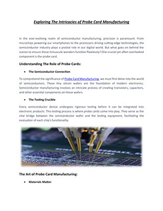
- 1. Exploring The Intricacies of Probe Card Manufacturing In the ever-evolving realm of semiconductor manufacturing, precision is paramount. From microchips powering our smartphones to the processors driving cutting-edge technologies, the semiconductor industry plays a pivotal role in our digital world. But what goes on behind the scenes to ensure these minuscule wonders function flawlessly? One crucial yet often overlooked component is the probe card. Understanding The Role of Probe Cards: • The Semiconductor Connection To comprehend the significance of Probe Card Manufacturing, we must first delve into the world of semiconductors. These tiny silicon wafers are the foundation of modern electronics. Semiconductor manufacturing involves an intricate process of creating transistors, capacitors, and other essential components on these wafers. • The Testing Crucible Every semiconductor device undergoes rigorous testing before it can be integrated into electronic products. This testing process is where probe cards come into play. They serve as the vital bridge between the semiconductor wafer and the testing equipment, facilitating the evaluation of each chip's functionality. The Art of Probe Card Manufacturing: • Materials Matter
- 2. The journey of a probe card begins with the selection of materials. To ensure optimal performance and longevity, manufacturers typically use materials like tungsten, ceramic, and various types of coatings. Each material choice carries specific advantages, contributing to the card's overall effectiveness. • Precision Crafting Manufacturing a probe card is no simple task. The process involves intricate machining and etching, typically employing advanced technologies such as photolithography and chemical vapor deposition. The end result is a highly precise card with microscopic features that can accurately probe the tiniest components on a semiconductor wafer. • Customization is Key Probe cards are not one-size-fits-all. They are customized to match the specific needs of semiconductor manufacturers. This customization extends to the size and arrangement of probes, as well as the electrical characteristics of the card. Tailoring probe cards to suit different testing requirements is a delicate art. • Quality Assurance As with any component destined for the semiconductor industry, quality control is paramount. Probe card manufacturers adhere to strict quality standards to ensure that each card meets the desired specifications. This includes thorough inspections, testing, and calibration to guarantee accuracy and reliability. The Anatomy of a Probe Card: • Probing the Probes At the heart of a probe card are its probes, which are responsible for making contact with the semiconductor wafer. These probes must be incredibly fine and precisely aligned to ensure accurate testing. They come in various shapes and sizes, depending on the specific testing requirements. • The Ceramic Substrate The ceramic substrate serves as the foundation of the probe card. It provides stability and electrical insulation, preventing any interference during the testing process. The choice of ceramic material is critical, as it must withstand harsh conditions and temperature fluctuations. • Connector Interface
- 3. Probe cards are designed to connect seamlessly with testing equipment. The connector interface is a crucial component that ensures a secure and reliable connection. It must be designed to withstand repeated use without degradation in performance. • Precision Alignment The alignment of probes is a meticulous process. Even the slightest misalignment can result in inaccurate testing. Advanced alignment techniques are employed to achieve the required precision, often involving automated systems for consistent results. The Manufacturing Process Unveiled: • Design and Prototyping The journey of a probe card commences with meticulous design and prototyping. Engineers collaborate with semiconductor manufacturers to understand their testing needs and create a custom design. Prototyping allows for testing and refining the design before moving to production. • Material Selection Once the design is finalized, the appropriate materials are selected. Tungsten is often chosen for its excellent electrical conductivity, while ceramics offer durability. These materials are prepared and shaped according to the design specifications. • Precision Machining Precision machining is the cornerstone of probe card manufacturing. Advanced machinery is used to create the intricate features of the card, including the probe tips and substrate. This process demands high levels of accuracy to ensure the card's functionality. • Etching and Coating Etching and coating processes are employed to enhance the performance of the probe card. Etching is used to refine the shape of the probes, while coatings may be applied to improve conductivity or protect against corrosion. • Assembly and Calibration With the individual components ready, the probe card is assembled. This includes attaching the probes to the ceramic substrate and integrating the connector interface. Once assembled, the card undergoes rigorous calibration to ensure precision and reliability.
- 4. • Quality Control Quality control checks are performed at various stages of manufacturing. These checks involve meticulous inspections, electrical testing, and alignment verification. Any deviations from the desired specifications are addressed promptly. • Customization Probe cards are tailored to specific semiconductor testing requirements. This customization involves configuring the number and arrangement of probes, as well as fine-tuning the electrical characteristics to match the intended application. • Packaging and Delivery Once a probe card passes all quality control checks and customization requirements, it is carefully packaged to prevent any damage during transit. These delicate instruments are then delivered to semiconductor manufacturers ready for action. The Evolution of Probe Card Technology: • Advancements in Materials Over the years, probe card manufacturers have continued to explore new materials and coatings to improve performance and longevity. This has led to the development of innovative materials that offer enhanced electrical conductivity and resistance to wear and tear. • Miniaturization and Higher Density As semiconductor technology advances, the components on wafers become smaller and denser. To keep pace, probe cards have undergone a process of miniaturization. This involves reducing the size of probes and increasing their density to accommodate the finer features of modern semiconductors. • Automation and Robotics Manufacturing probe cards demand a high degree of precision, making them an ideal candidate for automation. Robotics and advanced machinery have been integrated into the production process to ensure consistent quality and efficiency. • Enhanced Calibration Techniques
- 5. Calibrating probe cards is a critical step to guarantee accuracy. Advancements in calibration techniques, including the use of laser systems and computer-assisted algorithms, have improved the precision of probe cards. The Future of Probe Card Manufacturing: • Integration with Industry 4.0 The Fourth Industrial Revolution, often referred to as Industry 4.0, is driving automation, data exchange, and smart technology integration across industries. Probe Card Manufacturer is no exception. The integration of Industry 4.0 principles is expected to streamline production, reduce errors, and enhance overall efficiency. • AI and Machine Learning Artificial intelligence (AI) and machine learning are poised to play a significant role in probe card manufacturing. These technologies can optimize design, predict maintenance needs, and even assist in quality control by analyzing vast datasets. • Sustainability Initiatives As the world becomes increasingly environmentally conscious, Probe Card Manufacturers are exploring sustainable materials and manufacturing processes. This includes reducing waste and energy consumption, as well as recycling materials wherever possible. Conclusion: In the world of semiconductor manufacturing, where precision is the key to success, probe cards are unsung heroes. These unassuming devices play a pivotal role in ensuring the functionality and reliability of the tiny wonders that power our digital world. With advancements in materials, technology, and customization, probe card manufacturing continues to evolve, paving the way for the semiconductor industry to push the boundaries of innovation. As we move forward, the integration of smart technologies and sustainable practices promises to further enhance the efficiency and eco-friendliness of probe card manufacturing, ensuring its continued relevance in our ever-connected world.