The Art and Science of Probe Card Design in California
•
0 likes•2 views

The Art and Science of Probe Card Design in California

Recommended
Recommended
More Related Content
Similar to The Art and Science of Probe Card Design in California
Similar to The Art and Science of Probe Card Design in California (20)
More from Semi Probes Inc
More from Semi Probes Inc (20)
Recently uploaded
Recently uploaded (20)
The Art and Science of Probe Card Design in California
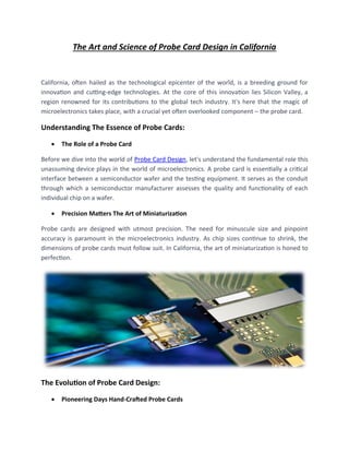
- 1. The Art and Science of Probe Card Design in California California, often hailed as the technological epicenter of the world, is a breeding ground for innovation and cutting-edge technologies. At the core of this innovation lies Silicon Valley, a region renowned for its contributions to the global tech industry. It's here that the magic of microelectronics takes place, with a crucial yet often overlooked component – the probe card. Understanding The Essence of Probe Cards: • The Role of a Probe Card Before we dive into the world of Probe Card Design, let's understand the fundamental role this unassuming device plays in the world of microelectronics. A probe card is essentially a critical interface between a semiconductor wafer and the testing equipment. It serves as the conduit through which a semiconductor manufacturer assesses the quality and functionality of each individual chip on a wafer. • Precision Matters The Art of Miniaturization Probe cards are designed with utmost precision. The need for minuscule size and pinpoint accuracy is paramount in the microelectronics industry. As chip sizes continue to shrink, the dimensions of probe cards must follow suit. In California, the art of miniaturization is honed to perfection. The Evolution of Probe Card Design: • Pioneering Days Hand-Crafted Probe Cards
- 2. In the early days of semiconductor manufacturing, probe cards were often crafted by skilled technicians who painstakingly assembled them by hand. Each probe was carefully positioned, and the card itself was customized for specific applications. These artisans played a vital role in the industry's infancy. • Automation Takes Over As demand for semiconductors skyrocketed, manual craftsmanship became insufficient. This gave rise to the automation of probe card design. In California's tech labs, engineers and scientists were at the forefront of developing automated manufacturing processes for probe cards, streamlining production and ensuring consistency. • Materials Matter The Quest for Durability Probe card designers continually seek materials that can withstand the rigors of semiconductor testing. California's tech-driven environment has driven the development of innovative materials, ensuring probe cards endure the challenges posed by high temperatures, high currents, and extreme conditions. The Precision Engineering Behind Probe Cards: • Designing for Compatibility Probe cards are tailored to specific semiconductor testing equipment, making compatibility a top priority. California-based engineers work closely with equipment manufacturers to ensure seamless integration, optimizing efficiency in the testing process. • Multi-Die Testing A Complex Challenge With the advent of multi-die semiconductor packages, the complexity of probe card design has grown exponentially. Engineers in California are constantly innovating to create probe cards capable of testing multiple dies simultaneously, further pushing the boundaries of microelectronics. • Precision Alignment The Key to Success One of the most critical aspects of probe card design is the alignment of the probes with the semiconductor wafer. Even a minuscule misalignment can lead to inaccurate test results. In California, cutting-edge technologies such as laser alignment systems have revolutionized this aspect of probe card design, ensuring unparalleled accuracy. The Crucial Role of Calibration:
- 3. • Calibrating for Perfection Calibration is the process by which a probe card's performance is fine-tuned to achieve optimal accuracy. In California, state-of-the-art calibration facilities are equipped with advanced instrumentation and highly skilled technicians who meticulously adjust the probe card's parameters to ensure it functions flawlessly. • Continuous Improvement The California Way The tech industry is relentless in its pursuit of perfection. Probe card designers in California understand that calibration is not a one-time process but an ongoing endeavor. As semiconductor technology advances, so must the precision and calibration of probe cards to keep pace. Innovations in Probe Card Technology: • The Rise of MEMS Probe Cards Micro-electro-mechanical systems (MEMS) probe cards have emerged as a revolutionary development in the field. These probe cards leverage MEMS technology to achieve unparalleled precision and flexibility in testing a wide range of semiconductor devices. California's tech companies are at the forefront of this MEMS revolution. • Advanced Materials The Future of Probe Cards Materials science continues to play a pivotal role in the evolution of probe card design. In California, researchers are exploring novel materials that offer enhanced electrical conductivity, durability, and resistance to wear and tear, ensuring that probe cards remain reliable even in the most demanding testing environments. The Human Touch Skilled Professionals in California: • The Engineer's Perspective Behind every cutting-edge probe card is a team of dedicated engineers and scientists. In California, these professionals are not just designers but visionaries who shape the future of microelectronics. Their expertise, creativity, and relentless pursuit of excellence drive the evolution of probe card technology. • The Technician's Precision
- 4. While automation has streamlined many aspects of probe card manufacturing, technicians still play a vital role in assembling and fine-tuning these critical devices. Their attention to detail and commitment to quality ensure that each probe card meets the highest standards of performance. The Future of Probe Card Design: • The Quantum Leap Quantum Computing As the tech industry sets its sights on quantum computing, the role of probe cards is poised to expand. California's research institutions and tech giants are already exploring how Probe Cards Supplies can be adapted for quantum devices, opening up new frontiers in testing and measurement. • Sustainability in Design In an era where environmental sustainability is paramount, probe card designers in California are working to develop eco-friendly materials and manufacturing processes. The aim is to reduce the environmental footprint of probe cards while maintaining their exceptional performance. Conclusion: In the heart of California's Silicon Valley, probe cards may not be the most celebrated technology, but they are undeniably the unsung heroes of the microelectronics industry. These unassuming devices, born from a rich history of innovation, continue to evolve in step with the relentless progress of technology, ensuring that the chips powering our digital world meet the highest standards of quality and performance. As California remains at the forefront of technological advancement, so too will its probe card designers, shaping the future of microelectronics one precision-engineered card at a time.