The Art of Probe Card Design in California A Journey into Precision and Innovation
•
0 likes•2 views

The Art of Probe Card Design in California A Journey into Precision and Innovation

Recommended
Recommended
More Related Content
Similar to The Art of Probe Card Design in California A Journey into Precision and Innovation
Similar to The Art of Probe Card Design in California A Journey into Precision and Innovation (20)
More from Semi Probes Inc
More from Semi Probes Inc (20)
Recently uploaded
Recently uploaded (20)
The Art of Probe Card Design in California A Journey into Precision and Innovation
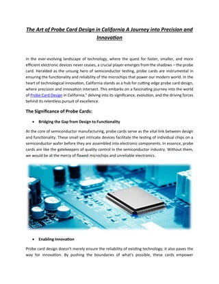
- 1. The Art of Probe Card Design in California A Journey into Precision and Innovation In the ever-evolving landscape of technology, where the quest for faster, smaller, and more efficient electronic devices never ceases, a crucial player emerges from the shadows – the probe card. Heralded as the unsung hero of semiconductor testing, probe cards are instrumental in ensuring the functionality and reliability of the microchips that power our modern world. In the heart of technological innovation, California stands as a hub for cutting-edge probe card design, where precision and innovation intersect. This embarks on a fascinating journey into the world of Probe Card Design in California," delving into its significance, evolution, and the driving forces behind its relentless pursuit of excellence. The Significance of Probe Cards: • Bridging the Gap from Design to Functionality At the core of semiconductor manufacturing, probe cards serve as the vital link between design and functionality. These small yet intricate devices facilitate the testing of individual chips on a semiconductor wafer before they are assembled into electronic components. In essence, probe cards are like the gatekeepers of quality control in the semiconductor industry. Without them, we would be at the mercy of flawed microchips and unreliable electronics. • Enabling Innovation Probe card design doesn't merely ensure the reliability of existing technology; it also paves the way for innovation. By pushing the boundaries of what's possible, these cards empower
- 2. engineers and designers to create smaller, faster, and more efficient electronic devices. In California, a hotbed of innovation, probe card designers are constantly exploring new materials, technologies, and methodologies to stay at the forefront of the industry. The Evolution of Probe Card Design: 1. From Simple Beginnings The history of probe cards can be traced back to the early days of the semiconductor industry when electronic devices were in their infancy. Initially, probe cards were rudimentary, featuring a small number of needles or probes that made contact with the semiconductor wafer's bond pads. These early designs were effective for their time but lacked the precision required for today's complex microchips. 2. The Era of Advancement As technology advanced, so did probe card design. In the mid-20th century, the introduction of integrated circuits (ICs) led to the need for more advanced testing methods. This necessitated the development of more sophisticated probe cards with a higher number of probes and greater precision. California played a pivotal role in this era of advancement, with companies in Silicon Valley leading the charge. 3. The Modern Marvels Today, probe card design has reached unprecedented levels of sophistication. These modern marvels are meticulously engineered, featuring thousands of tiny probes that can make contact with individual bond pads on a semiconductor wafer. They are capable of testing multiple chips simultaneously, dramatically increasing efficiency and throughput. The precision and reliability of these cards are paramount, as even the slightest deviation can result in faulty chips. The Anatomy of a Probe Card: • Probing the Probes At the heart of every probe card are, well, the probes. These are the tiny, needle-like structures that make contact with the bond pads on a semiconductor wafer. Probes come in various shapes and sizes, depending on the specific requirements of the testing process. The materials used for probes are carefully chosen to ensure durability, conductivity, and resistance to wear and tear. • The Substrate Surrounding the probes is the substrate, which serves as the foundation of the probe card. The substrate is typically made of a high-quality, non-conductive material, such as ceramic or epoxy
- 3. resin. Its role is to provide structural support for the probes and to distribute electrical signals from the probes to the testing equipment. • Precision Alignment One of the most critical aspects of probe card design is precision alignment. The probes must be meticulously arranged to ensure that they make accurate and consistent contact with the bond pads on the semiconductor wafer. Even the tiniest misalignment can lead to testing errors and the production of defective chips. • Temperature Control In some cases, temperature control mechanisms are integrated into probe cards. This is particularly important in applications where temperature variations can affect testing accuracy. Temperature-controlled probe cards ensure that testing conditions remain stable, even in demanding environments. Innovation in Probe Card Design: • Miniaturization One of the key trends in probe card design is miniaturization. As electronic devices continue to shrink in size, probe cards must follow suit. This requires the development of smaller and more densely packed probes that can access the bond pads on increasingly compact semiconductor wafers. • Advanced Materials California's role as an innovation hub extends to the exploration of advanced materials for probe card design. Researchers and engineers are constantly seeking materials that offer superior electrical conductivity, durability, and resistance to wear. Carbon nanotubes and advanced polymers are among the materials being investigated for their potential in probe card construction. • Automation and Robotics Automation is another area where probe card design is making significant strides. Automated probe card handling and testing systems are being developed to streamline the testing process and increase efficiency. Robotics play a crucial role in these systems, allowing for precise and repeatable testing procedures. • Artificial Intelligence Integration
- 4. Artificial intelligence (AI) is also making its presence felt in probe card design. AI algorithms can analyze vast amounts of testing data and identify patterns and anomalies that may be missed by human operators. This not only improves testing accuracy but also helps in identifying and resolving production issues more efficiently. California's Leading Role in Probe Card Design: • Silicon Valley The Epicenter of Innovation When we think of technological innovation, Silicon Valley immediately comes to mind. This region in California has long been synonymous with cutting-edge developments in the Semiconductor Industry, including probe card design. It's home to some of the world's most renowned technology companies and research institutions, making it the ideal breeding ground for innovation in this field. • Collaboration and Knowledge Sharing California's prominence in probe card design is also attributed to the spirit of collaboration and knowledge sharing that permeates the region. Companies and research organizations in Silicon Valley frequently collaborate on research projects, share expertise, and pool resources to advance probe card technology collectively. Challenges and Future Prospects: 1. The Challenge of Moore's Law One of the significant challenges facing probe card designers is keeping pace with Moore's Law. This observation, made by Gordon Moore in 1965, predicts that the number of transistors on a microchip will double approximately every two years. As semiconductor technology continues to shrink, probe cards must become even more precise and capable to test these densely packed chips effectively. 2. Sustainability Concerns In an era of increasing environmental consciousness, sustainability concerns are also impacting probe card design. There is a growing emphasis on developing probe cards that are not only efficient but also environmentally friendly. This includes using eco-friendly materials, optimizing manufacturing processes, and reducing waste. 3. Security and Cybersecurity With the increasing connectivity of electronic devices, security, and cybersecurity have become paramount concerns. Probe card designers must ensure that their products are not vulnerable
- 5. to tampering or malicious attacks. This requires the integration of security features and robust cybersecurity measures into probe card design. Conclusion: Probe card design in California stands as a testament to the indomitable spirit of innovation and precision in the semiconductor industry. From its humble beginnings to its current state of sophistication, probe cards have played a pivotal role in ensuring the reliability and functionality of the electronic devices we rely on daily. As technology continues to advance at an unprecedented pace, the future of probe card design promises to be a thrilling journey, driven by innovation