Unlocking the Potential of Vertical Probe Cards and Best Practices and Case Studies from Santa Clara
•
0 likes•2 views

Unlocking the Potential of Vertical Probe Cards and Best Practices and Case Studies from Santa Clara.

Recommended
Recommended
More Related Content
Similar to Unlocking the Potential of Vertical Probe Cards and Best Practices and Case Studies from Santa Clara
Similar to Unlocking the Potential of Vertical Probe Cards and Best Practices and Case Studies from Santa Clara (20)
More from Semi Probes Inc
More from Semi Probes Inc (20)
Recently uploaded
Recently uploaded (20)
Unlocking the Potential of Vertical Probe Cards and Best Practices and Case Studies from Santa Clara
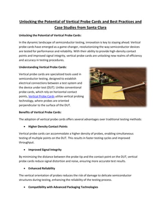
- 1. Unlocking the Potential of Vertical Probe Cards and Best Practices and Case Studies from Santa Clara Unlocking the Potential of Vertical Probe Cards: In the dynamic landscape of semiconductor testing, innovation is key to staying ahead. Vertical probe cards have emerged as a game-changer, revolutionizing the way semiconductor devices are tested for performance and reliability. With their ability to provide high-density contact points and improved signal integrity, vertical probe cards are unlocking new realms of efficiency and accuracy in testing procedures. Understanding Vertical Probe Cards: Vertical probe cards are specialized tools used in semiconductor testing, designed to establish electrical connections between a test system and the device under test (DUT). Unlike conventional probe cards, which rely on horizontal contact points, Vertical Probe Cards utilize vertical probing technology, where probes are oriented perpendicular to the surface of the DUT. Benefits of Vertical Probe Cards: The adoption of vertical probe cards offers several advantages over traditional testing methods: • Higher Density Contact Points Vertical probe cards can accommodate a higher density of probes, enabling simultaneous testing of multiple points on the DUT. This results in faster testing cycles and improved throughput. • Improved Signal Integrity By minimizing the distance between the probe tip and the contact point on the DUT, vertical probe cards reduce signal distortion and noise, ensuring more accurate test results. • Enhanced Reliability The vertical orientation of probes reduces the risk of damage to delicate semiconductor structures during testing, enhancing the reliability of the testing process. • Compatibility with Advanced Packaging Technologies
- 2. Vertical probe cards are well-suited for testing advanced packaging technologies such as 3D ICs and wafer-level packaging, enabling comprehensive testing of complex semiconductor devices. Best Practices for Vertical Probe Card Testing: To harness the full potential of vertical probe cards, semiconductor manufacturers must adhere to best practices in testing procedures: • Optimize Probe Design Customizing probe designs to match the specific requirements of the DUT can significantly improve testing accuracy and efficiency. Fine-tuning parameters such as probe material, tip geometry, and spring force is essential for achieving optimal performance. • Maintain Cleanroom Environment Contaminants such as dust particles can interfere with the electrical connections established by vertical probe cards. Maintaining a cleanroom environment and implementing appropriate cleaning protocols are crucial for minimizing the risk of probe contamination. • Implement Robust Calibration Procedures Regular calibration of vertical probe cards is essential for ensuring accurate and reliable test results. Calibration procedures should account for factors such as probe wear, temperature variations, and contact resistance to maintain the integrity of the testing system. • Monitor Probe Health Monitoring the health and performance of individual probes is essential for preventing premature failures and ensuring consistent testing quality. Implementing proactive probe health monitoring systems allows for timely identification and replacement of faulty probes. Case Studies from Santa Clara: Santa Clara, a hub of semiconductor innovation, has been at the forefront of adopting vertical probe card technology. Let's explore some real-world case studies showcasing the transformative impact of vertical probe cards in semiconductor testing: • High-Volume Production Testing A leading semiconductor manufacturer in Santa Clara deployed vertical probe cards in its high- volume production testing facility. By leveraging the high-density contact points offered by vertical probe cards, the manufacturer achieved a significant increase in testing throughput, enabling faster time-to-market for its semiconductor products.
- 3. • Testing of Advanced Packaging Technologies Another semiconductor company based in Santa Clara utilized vertical probe cards for testing advanced packaging technologies such as 3D ICs and stacked dies. The superior signal integrity and compatibility of Vertical Probe Cards with complex packaging structures allowed the company to conduct comprehensive testing of its cutting-edge semiconductor devices, ensuring robust performance and reliability. Conclusion: Vertical probe cards represent a paradigm shift in semiconductor testing, offering unparalleled efficiency, accuracy, and reliability. By adopting best practices and learning from real-world case studies, semiconductor manufacturers can unlock the full potential of vertical probe cards, driving innovation and excellence in the semiconductor industry. As Santa Clara continues to spearhead technological advancements in semiconductor testing, vertical probe cards are poised to play a pivotal role in shaping the future of semiconductor manufacturing.