Probe Card Manufacturing Unveiling The Technology Behind Semiconductor Testing
•
0 likes•5 views

Probe Card Manufacturing Unveiling The Technology Behind Semiconductor Testing

Recommended
Recommended
More Related Content
Similar to Probe Card Manufacturing Unveiling The Technology Behind Semiconductor Testing
Similar to Probe Card Manufacturing Unveiling The Technology Behind Semiconductor Testing (20)
More from Semi Probes Inc
More from Semi Probes Inc (20)
Recently uploaded
Recently uploaded (20)
Probe Card Manufacturing Unveiling The Technology Behind Semiconductor Testing
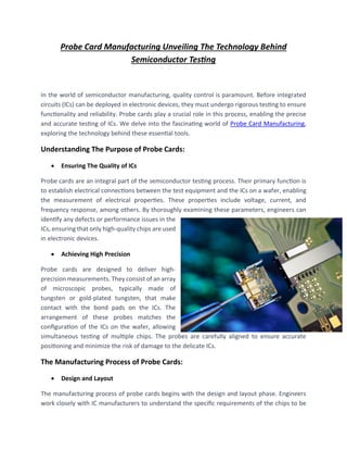
- 1. Probe Card Manufacturing Unveiling The Technology Behind Semiconductor Testing In the world of semiconductor manufacturing, quality control is paramount. Before integrated circuits (ICs) can be deployed in electronic devices, they must undergo rigorous testing to ensure functionality and reliability. Probe cards play a crucial role in this process, enabling the precise and accurate testing of ICs. We delve into the fascinating world of Probe Card Manufacturing, exploring the technology behind these essential tools. Understanding The Purpose of Probe Cards: • Ensuring The Quality of ICs Probe cards are an integral part of the semiconductor testing process. Their primary function is to establish electrical connections between the test equipment and the ICs on a wafer, enabling the measurement of electrical properties. These properties include voltage, current, and frequency response, among others. By thoroughly examining these parameters, engineers can identify any defects or performance issues in the ICs, ensuring that only high-quality chips are used in electronic devices. • Achieving High Precision Probe cards are designed to deliver high- precision measurements. They consist of an array of microscopic probes, typically made of tungsten or gold-plated tungsten, that make contact with the bond pads on the ICs. The arrangement of these probes matches the configuration of the ICs on the wafer, allowing simultaneous testing of multiple chips. The probes are carefully aligned to ensure accurate positioning and minimize the risk of damage to the delicate ICs. The Manufacturing Process of Probe Cards: • Design and Layout The manufacturing process of probe cards begins with the design and layout phase. Engineers work closely with IC manufacturers to understand the specific requirements of the chips to be
- 2. tested. This includes factors such as the number and arrangement of bond pads, pitch sizes, and overall dimensions. Using specialized design software, the probe card layout is meticulously created, taking into account factors like probe density, routing complexity, and signal integrity. • Substrate Fabrication Once the probe card design is finalized, the next step is substrate fabrication. The substrate serves as the foundation for the probe card, providing mechanical support and electrical connectivity. The most commonly used material for probe card substrates is high-quality ceramic, such as alumina or silicon nitride. These materials offer excellent electrical insulation properties and mechanical stability. The substrate fabrication process involves several steps, including substrate cutting, polishing, and metallization. First, the ceramic material is cut into the desired shape and size using precision cutting tools. Next, the substrate surface is polished to ensure a smooth and flat surface for probe attachment. Finally, a thin layer of conductive material, typically copper or gold, is deposited onto the substrate surface using techniques like sputtering or electroplating. This metallization process forms the electrical traces and vias necessary for probe connectivity. • Probe Assembly The heart of the probe card lies in its probes. To assemble the probes, specialized equipment and techniques are employed. First, a probe holder, often made of ceramic or plastic, is prepared. The holder provides the necessary support for the probes and helps maintain their alignment. Next, individual probes, typically made of tungsten wire, are attached to the holder using techniques like epoxy bonding or ultrasonic welding. The alignment of the probes is crucial at this stage to ensure proper contact with the bond pads on the ICs. • Testing and Inspection Once the probe assembly is complete, the probe card undergoes rigorous testing and inspection procedures. This ensures that the electrical connections are intact, the probes are aligned correctly, and there are no manufacturing defects. Various electrical tests are performed to measure parameters like resistance and capacitance, validating the integrity of the probe card. Additionally, visual inspection and optical microscopy are utilized to examine the probes for any physical abnormalities or damages. Advancements in Probe Card Manufacturing: • Miniaturization and High-Density Probing
- 3. As IC technology continues to advance, the demand for smaller and more densely packed chips grows. This trend has pushed the boundaries of probe card manufacturing, requiring ever-smaller probes and higher probe densities. To address this challenge, manufacturers have developed innovative techniques such as MEMS (Micro-Electro-Mechanical Systems) and advanced lithography. These advancements enable the production of ultra-miniature probes with nanometer-scale dimensions, allowing for highly precise probing of next-generation ICs. • Multi-DUT (Device Under Test) Testing Traditional probe cards typically enable the testing of a single chip at a time. However, with the increasing complexity and parallelism of modern IC designs, there is a growing need for simultaneous testing of multiple chips on a wafer. To address this demand, probe card manufacturers have introduced multi-DUT probe cards. These cards feature an array of probes that can make contact with multiple chips simultaneously, significantly reducing testing time and increasing throughput. • Advanced Material Selection To meet the evolving requirements of semiconductor testing, probe card manufacturers are constantly exploring new materials for improved performance and longevity. For instance, some manufacturers are experimenting with composite materials that offer enhanced electrical conductivity and mechanical durability. Additionally, novel coating techniques are being employed to reduce wear and tear on the probes, prolonging their lifespan and ensuring consistent contact reliability. Conclusion: Probe card manufacturing plays a critical role in the semiconductor industry, enabling comprehensive testing of ICs before their integration into electronic devices. The precise and reliable measurement capabilities of Probe Cards ensure that only high-quality chips make their way into the market, enhancing the overall reliability and performance of electronic devices. As technology continues to advance, the probe card industry will undoubtedly push the boundaries of miniaturization, density, and material advancements, further improving the efficiency and accuracy of semiconductor testing.