
Recommended
More Related Content
What's hot
What's hot (20)
Viewers also liked
Viewers also liked (12)
Similar to Transistor, fotodiode, dan diode pemencar [14]
Similar to Transistor, fotodiode, dan diode pemencar [14] (20)
Recently uploaded
Recently uploaded (20)
Transistor, fotodiode, dan diode pemencar [14]
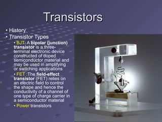
- 1. TransistorsTransistors • History • Transistor Types • BJT: A bipolar (junction) transistor is a three- terminal electronic device constructed of doped semiconductor material and may be used in amplifying or switching applications • FET :The field-effect transistor (FET) relies on an electric field to control the shape and hence the conductivity of a channel of one type of charge carrier in a semiconductor material • Power transistors
- 2. What is a Transistor? A Transistor is an electronic device composed of layers of a semiconductor material which regulates current or voltage flow and acts as a switch or gate for electronic circuit.
- 3. History of the Transistor John Pierce –supervised the BellJohn Pierce –supervised the Bell Labs team which built the firstLabs team which built the first transistor (1947)transistor (1947) First Solid State Transistor – (1951) Gordon K. Teal (left) and Morgan Sparks at Bell Laboratories, 1951 Akio Morita, who founded a newAkio Morita, who founded a new company named Sony Electronicscompany named Sony Electronics that mass-produced tinythat mass-produced tiny transistorized radios (1961)transistorized radios (1961)
- 6. Composed of N and P-type Semiconductors • N-type Semiconductor has an excess of electrons – Doped with impurity with more valence electrons than silicon P-type Semiconductor has a deficit of electrons (Holes) – Doped with impurity with less valence electrons than silicon
- 7. P-N Junction (Basic diode): - Bringing P and N Semiconductors in contact P Type N Type - Creation of a Depletion Zone
- 8. Reverse Biased => No Current Applying –Voltage to Anode increases Barrier Voltage & Inhibits Current Flow • Applying Voltage to Cathode • Barrier Voltage to Anode allows current flow Forward Biased => Current
- 9. Types Of TransistorsTypes Of Transistors NPN: transistor where the majority current carriers are electrons The majority current carriers in the PNP transistor are holes
- 11. California Test QuestionsCalifornia Test Questions A transistor circuit is used as an amplifier. When a signal is applied to the input of the transistor, the output signal is A a smaller amplitude. B an equal amplitude. C a larger amplitude. D zero amplitude. C: The collector and emitter will amplify the output signal from the Bias input.
- 12. California Test QuestionsCalifornia Test Questions A transistor is classified as a semiconductor because: A the transistor conducts electricity. B the transistor increases the amplitude. C the transistor increases the frequency. D intentionally introducing impurities into an extremely pure silicon or germanium.silicon or germanium. D intentionally introducing impurities into an extremely pure silicon or germanium.silicon or germanium.
- 13. SummarySummary Transistors are composed of three parts – aTransistors are composed of three parts – a base, a collector, and an emitter .base, a collector, and an emitter . Semi-conductive materials are what make theSemi-conductive materials are what make the transistor possible .transistor possible . There are two main types of transistors-junctionThere are two main types of transistors-junction transistors and field effect transistors.transistors and field effect transistors. Field effect transistor has only two layers ofField effect transistor has only two layers of semiconductor material, one on top of the othersemiconductor material, one on top of the other
- 14. 4/11/2006 BAE 5413 14 Application of photodiodes A brief overview
- 15. 4/11/2006 BAE 5413 15 Diode devices • Check valve behavior – Diffusion at the PN junction of P into N and N into P causes a depleted non- conductive region – Depletion is enhanced by reverse bias – Depletion is broken down by forward bias • When forward biased – High current flow junction voltage • When reverse biased – Very low current flow unless above peak inverse voltage (PIV) (damaging to rectifying diodes, OK for zeners)
- 16. 4/11/2006 BAE 5413 16 Quantum devices • Absorption of a photon of sufficient energy elevates an electron into the conduction band and leaves a hole in the valence band. • Conductivity of semi-conductor is increased. • Current flow in the semi-conductor is induced.
- 17. 4/11/2006 BAE 5413 17 Photodiode structure Absorbtion in the depletion layer causses current to flow across the photodiode and if the diode is reverse biased considerable current flow will be induced
- 18. 4/11/2006 BAE 5413 18 Photodiode fundamentals • Based on PN or PIN junction diode – photon absorption in the depletion region induces current flow – Depletion layer must be exposed optically to source light and thick enough to interact with the light • Spectral sensitivity Material Band gap (eV) Spectral sensitivity silicon (Si) 1.12 250 to 1100 nm indium arsenide (InGaAs) ~0.35 1000 to 2200 nm Germanium (Ge) .67 900 to 1600 nm
- 19. 4/11/2006 BAE 5413 19 Photodiode characteristics • Circuit model – I0 Dark current (thermal) – Ip Photon flux related current • Noise characterization – Shot noise (signal current related) – q = 1.602 x 10⁻¹⁹ coulombs – I = bias (or signal) current (A) – is = noise current (A rms) – Johnson noise (Temperature related) – k = Boltzman’s constant = 1.38 x 10⁻²³ J/K – T = temperature (°K) – B = noise bandwidth (Hz) – R = feedback resistor (W) – eOUT = noise voltage (Vrms) qiis 2= kTBReout 4=
- 20. 4/11/2006 BAE 5413 20 Photodiode current/voltage characteristics
- 21. 4/11/2006 BAE 5413 21 Trans-impedance amplifier function • Current to voltage converter (amplifier) • Does not bias the photodiode with a voltage as current flows from the photodiode (V1 = 0) • Circuit analysis sf II −= 0≈oI 01 ≈V sffff IRIRV −== sffout IRVV −== –Note: current to voltage conversion
- 22. 4/11/2006 BAE 5413 22 Diode operating modes • Photovoltaic mode – Photodiode has no bias voltage – Lower noise – Lower bandwidth – Logarithmic output with light intensity • Photoconductive mode – Higher bandwidth – Higher noise – Linear output with light intensity
- 23. 4/11/2006 BAE 5413 23 For the photovoltaic mode • I = thermal component + photon flux related current • where I = photodiode current V = photodiode voltage I0 = reverse saturation current of diode e = electron charge k = Boltzman's constant T = temperature (K) ν = frequency of light h = Plank’s constant P = optical power η = probability that hv will elevate an electron across the band gap ν η h eP eII kT eV − −= 10
- 24. 4/11/2006 BAE 5413 24 Circuit Optimization • Burr-Brown recommendations (TI) • Photodiode capacitance should be as low as possible. • Photodiode active area should be as small as possible so that CJ is small and RJ is high. • Photodiode shunt resistance (RJ ) should be as high as possible. • For highest sensitivity use the photodiode in a “photovoltaic mode”. • Use as large a feedback resistor as possible (consistent with bandwidth requirements) to minimize noise. • Shield the photodetector circuit in a metal housing. • A small capacitor across Rf is frequently required to suppress oscillation or gain peaking. • A low bias current op amp is needed to achieve highest sensitivity
- 25. THE LIGHT EMITTINGTHE LIGHT EMITTING DIODEDIODE Chapter 6Chapter 6
- 26. CB VB When the electronWhen the electron falls down fromfalls down from conduction band andconduction band and fills in a hole infills in a hole in valence band, there isvalence band, there is an obvious loss ofan obvious loss of energy.energy. The question is;The question is; where does that energy go?where does that energy go?
- 27. In order to achieve aIn order to achieve a reasonable efficiencyreasonable efficiency for photon emission,for photon emission, the semiconductorthe semiconductor must have a directmust have a direct band gap.band gap. CB VB The question is;The question is; what is the mechanismwhat is the mechanism behind photon emission in LEDs?behind photon emission in LEDs?
- 28. For example;For example; SiliconSilicon is known as anis known as an indirect band-gapindirect band-gap material.material. as an electron goes from the bottom ofas an electron goes from the bottom of the conduction band to the top of thethe conduction band to the top of the valence band;valence band; it must also undergo ait must also undergo a significantsignificant change inchange in momentum.momentum. CB VB What this means is thatWhat this means is that E k
- 29. As we all know, whenever something changesAs we all know, whenever something changes state, one must conserve not only energy, butstate, one must conserve not only energy, but also momentum.also momentum. In the case of an electron going fromIn the case of an electron going from conduction band to the valence band in silicon,conduction band to the valence band in silicon, both of these things can only be conserved:both of these things can only be conserved: The transition also creates a quantized set of lattice vibrations, called phonons, or "heat“ .
- 30. Phonons possess both energy and momentum.Phonons possess both energy and momentum. Their creation upon the recombination of anTheir creation upon the recombination of an electron and hole allows for completeelectron and hole allows for complete conservation of both energy and momentum.conservation of both energy and momentum. All of the energy which the electron gives up inAll of the energy which the electron gives up in going from the conduction band to the valencegoing from the conduction band to the valence band (1.1 eV) ends up in phonons, which isband (1.1 eV) ends up in phonons, which is another way of saying that the electron heats upanother way of saying that the electron heats up the crystal.the crystal.
- 31. In a class of materials calledIn a class of materials called direct band-gapdirect band-gap semiconductorssemiconductors;; the transition from conduction bandthe transition from conduction band to valence band involves essentiallyto valence band involves essentially no change in momentumno change in momentum.. Photons, it turns out, possess a fairPhotons, it turns out, possess a fair amount of energy ( several eV/photonamount of energy ( several eV/photon in some cases ) but they have veryin some cases ) but they have very little momentum associated withlittle momentum associated with them.them.
- 32. Thus, for a direct band gap material, the excessThus, for a direct band gap material, the excess energy of the electron-hole recombination canenergy of the electron-hole recombination can either be taken away as heat, or more likely, aseither be taken away as heat, or more likely, as a photon of light.a photon of light. This radiative transition thenThis radiative transition then conserves energy and momentumconserves energy and momentum by giving off light whenever anby giving off light whenever an electron and hole recombine.electron and hole recombine. CB VB This gives rise toThis gives rise to (for us) a new type(for us) a new type of device;of device; the light emitting diode (LED).the light emitting diode (LED).
- 33. Mechanism is “injectionMechanism is “injection Electroluminescence”.Electroluminescence”. LuminescenceLuminescence part tells us that we are producing photons.part tells us that we are producing photons. Electro part tells us thatElectro part tells us that the photons are being producedthe photons are being produced by an electric current.by an electric current. e- Injection tells us thatInjection tells us that photon production is byphoton production is by the injection of current carriers.the injection of current carriers. Mechanism behind photonMechanism behind photon emission in LEDs?emission in LEDs? e-
- 34. Producing photonProducing photon Electrons recombine with holes.Electrons recombine with holes. Energy of photon is the energy ofEnergy of photon is the energy of band gap.band gap. CB VB e- h
- 35. Method of injectionMethod of injection We need putting a lot of eWe need putting a lot of e-- ’s where there are lots’s where there are lots of holes.of holes. So electron-hole recombination can occur.So electron-hole recombination can occur. Forward biasing a p-n junction will inject lots of eForward biasing a p-n junction will inject lots of e-- ’s’s from n-side, across the depletion region into the p-from n-side, across the depletion region into the p- side where they will be combine with the highside where they will be combine with the high density of majority carriers.density of majority carriers. n-side p-side - + I
- 36. Notice that:Notice that: Photon emission occurs whenever we havePhoton emission occurs whenever we have injected minority carriers recombining with theinjected minority carriers recombining with the majority carriers.majority carriers. If the eIf the e-- diffusion length is greater than the holediffusion length is greater than the hole diffusion length, the photon emitting region willdiffusion length, the photon emitting region will be bigger on the p-side of the junction than thatbe bigger on the p-side of the junction than that of the n-side.of the n-side. Constructing a real LED may be best to considerConstructing a real LED may be best to consider a na n++++ p structure.p structure. It is usual to find the photon emitting volumeIt is usual to find the photon emitting volume occurs mostly on one side of the junction region.occurs mostly on one side of the junction region. This applies to LASER devices as well as LEDs.This applies to LASER devices as well as LEDs.
- 37. MATERIALS FOR LEDSMATERIALS FOR LEDS The semiconductor bandgapThe semiconductor bandgap energy defines the energy of theenergy defines the energy of the emitted photons in a LED.emitted photons in a LED. To fabricate LEDs that can emitTo fabricate LEDs that can emit photons from the infrared to thephotons from the infrared to the ultraviolet parts of the e.m.ultraviolet parts of the e.m. spectrum, then we must considerspectrum, then we must consider several different materialseveral different material systems.systems. No single system can span thisNo single system can span this energy band at present, althoughenergy band at present, although the 3-5 nitrides come close.the 3-5 nitrides come close. CB VB
- 38. Unfortunately, many of potentiallly useful 2-6Unfortunately, many of potentiallly useful 2-6 group of direct band-gap semiconductorsgroup of direct band-gap semiconductors (ZnSe,ZnTe,etc.)(ZnSe,ZnTe,etc.) come naturally dopedcome naturally doped either p-either p- type, or n-type, but they don’t like to be type-type, or n-type, but they don’t like to be type- converted by overdoping.converted by overdoping. The material reasons behind this areThe material reasons behind this are complicated and not entirely well-known.complicated and not entirely well-known. The same problem is encountered in the 3-5The same problem is encountered in the 3-5 nitrides and their alloys InN, GaN, AlN, InGaN,nitrides and their alloys InN, GaN, AlN, InGaN, AlGaN, and InAlGaN. The amazing thing aboutAlGaN, and InAlGaN. The amazing thing about 3-5 nitride alloy3-5 nitride alloy systems is that appear to besystems is that appear to be direct gapdirect gap throughout.throughout.
- 39. When we talk about light ,it is conventional toWhen we talk about light ,it is conventional to specify its wavelength,specify its wavelength, λλ, instead of its, instead of its frequency.frequency. Visible light has a wavelength on the order ofVisible light has a wavelength on the order of nanometers.nanometers. Thus, a semiconductor with a 2 eV band-gap should give a light at about 620 nm (in the red). A 3 eV band-gap material would emit at 414 nm, in the violet. The human eye, of course, is not equally responsive to all colors. ( ) ( ) hc nm E eV λ = 1242 ( ) ( ) nm E eV λ =
- 40. Relative response of the human eye to various colors 350 400 450 500 550 600 650 700 750 100 10-1 10-2 10-3 10-4 Relative eye responseRelative eye response Wavelength in nanometers The materials which are used for important light emitting diodes (LEDs) for each of the different spectral regions. GaNGaN ZnSeZnSe violet blue GaP:NGaP:N green yellow GaAsGaAs.14.14 pp 8686 GaAsGaAs.35.35 pp 6565 redorange GaAsGaAs.6.6 pp 44
- 41. Properties of InGaNProperties of InGaN InGaN alloy has one composition at a time only.InGaN alloy has one composition at a time only. This materialThis material will emit one wavelengthwill emit one wavelength onlyonly corresponding to this particular composition.corresponding to this particular composition. An InGaN LED wouldAn InGaN LED would not emit white lightnot emit white light (the(the whole of the visible spectrum at once) since itswhole of the visible spectrum at once) since its specific compositionspecific composition.. For aFor a white light sourcewhite light source we have to form awe have to form a complicated multilayercomplicated multilayer devicedevice emitting lots ofemitting lots of different wavelengths.different wavelengths.
- 42. Properties of InGaNProperties of InGaN A LED fabricatedA LED fabricated in ain a graded materialgraded material where on either side of the junction regionwhere on either side of the junction region thethe material changes slowly from InN tomaterial changes slowly from InN to GaNGaN via InGaN alloys.via InGaN alloys. Minority carriers need to get through theMinority carriers need to get through the whole of this alloy region if efficient photonwhole of this alloy region if efficient photon production at all visible wavelengths wasproduction at all visible wavelengths was to occur.to occur.
- 43. GaNGaN InNInN Concentration:Concentration: The highlyThe highly gallium richgallium rich alloyalloy The highlyThe highly indium richindium rich alloyalloy Band gap:Band gap: 3.3eV3.3eV 2 eV2 eV Wavelength ofWavelength of photons:photons: 376 nm376 nm 620 nm620 nm Part of thePart of the electromagneticelectromagnetic spectrum:spectrum: In the ultravioletIn the ultraviolet In the visibleIn the visible (orange)(orange)
- 45. GaN InN 3 eV (414 nm) violet
- 49. GaN InN 2.00 eV 2 eV(620 nm)
- 50. A number of the important LEDs are based on the GaAsP system. GaAsGaAs is a direct band-gap S/C with a band gap of 1.42 eV1.42 eV (in the infrared). GaPGaP is an indirect band-gap material with a band gap of 2.26 eV2.26 eV (550nm, or green). GaAs GaP 1.42 eV
- 51. GaAs GaP 1.52 eV
- 52. GaAs GaP 1.62 eV
- 53. GaAs GaP 1.72 eV
- 54. GaAs GaP 1.80 eV
- 55. GaAs GaP 1.90 eV
- 56. GaAs GaP 2.00 eV
- 57. GaAs GaP 2.26 eV
- 58. _ hν + Energy Momentum • Addition of a nitrogen recombination center to indirect GaAsP . Both As and P are group V elements. (Hence the nomenclature of the materials as III-V compound semiconductors.)
- 59. We can replace some of the As with P in GaAs and make a mixed compound semiconductor GaAs1-xPx. When the mole fraction of phosphorous is less than about 0.45 the band gap is direct, and so we can "engineer" the desired color of LED that we want by simply growing a crystal with the proper phosphorus concentration!
- 60. X CB Minimum Γ VB Maximum N Level Γ CB Minimum (a) Direct-gap GaAs N Level (b) Crossover GaAs0.50P0.50 N Level (c) Indirect-gap GaP Schematic band structure of GaAs, GaAsP, and GaP. Also shown is the nitrogen level. At a P mole fraction of about 45- 50 %, the direct-indirect crossover occurs.
- 61. Materials for visible wavelength LEDsMaterials for visible wavelength LEDs We see them almost everyday, either on calculatorWe see them almost everyday, either on calculator displays or indicator panels.displays or indicator panels. Red LED use as “ power on” indicatorRed LED use as “ power on” indicator Yellow, green and amber LEDs are also widely availableYellow, green and amber LEDs are also widely available but very few of you will have seen a blue LED.but very few of you will have seen a blue LED.
- 62. Red LEDsRed LEDs can be made in the GaAsPcan be made in the GaAsP (gallium arsenide phosphide).(gallium arsenide phosphide). GaAsGaAs1-x1-xPPxx for 0<x<0.45 has direct-gapfor 0<x<0.45 has direct-gap for x>0.45 the gap goesfor x>0.45 the gap goes indirect andindirect and for x=0.45 the band gapfor x=0.45 the band gap energy is 1.98 eV.energy is 1.98 eV. Hence it is useful for redHence it is useful for red LEDs.LEDs. N-GaAs substrate N-GaAsP P = 40 % p-GaAsP region Ohmic Contacts Dielectric (oxide or nitride) Fig. GaAsP RED LED on a GaAs sub.
- 63. Isoelectronic CentreIsoelectronic Centre IsoelectronicIsoelectronic means that tmeans that the centre being introducedhe centre being introduced has thehas the same number of valance electronssame number of valance electrons as the element it isas the element it is replacing.replacing. For example, nitrogen can replace some of the phosphorusFor example, nitrogen can replace some of the phosphorus in GaP. It is isoelectronic with phosphorus, butin GaP. It is isoelectronic with phosphorus, but behavesbehaves quite differentlyquite differently allowing reasonably efficient green emission.allowing reasonably efficient green emission.
- 64. How isoelectronic centres work?How isoelectronic centres work? For our isoelectronic centreFor our isoelectronic centre thethe position is very well-position is very well- defined,defined, hence there is ahence there is a considerableconsiderable spread in itsspread in its momentummomentum state.state. Isoelectronic centre has theIsoelectronic centre has the same valance configurationsame valance configuration as the phosphorus it isas the phosphorus it is replacing.replacing. It doesn't act as a dopantIt doesn't act as a dopant.. E dE Isoelectronic centre CB edge electrons Electron-hole recombination Holes VB edge k = 0
- 65. Isoelectronic centres provide a ‘Isoelectronic centres provide a ‘stepping stonestepping stone’ for’ for electrons in E-k space so that transitions can occurelectrons in E-k space so that transitions can occur that are radiatively efficient.that are radiatively efficient. The recombination eventThe recombination event shown has no change inshown has no change in momentum, so itmomentum, so it behaves like a directbehaves like a direct transition.transition. E dE Isoelectronic centre CB edge electrons Electron-hole recombination Holes VB edge k = 0 Because the effective transition is occurring betweenBecause the effective transition is occurring between the isoelectronic centre and VB edge, the photon thatthe isoelectronic centre and VB edge, the photon that is emitted has a lower energy than the band-gapis emitted has a lower energy than the band-gap energy.energy.
- 66. GaP : NGaP : N (dE = 50 meV) Photon energy(dE = 50 meV) Photon energy is less than the semiconductoris less than the semiconductor band-gap energy it means thatband-gap energy it means that the photon is not absorbed bythe photon is not absorbed by the semiconductor, and so thethe semiconductor, and so the photon is easily emitted fromphoton is easily emitted from the material.the material. This lack of absorption pushesThis lack of absorption pushes up the efficiency of the diodeup the efficiency of the diode as a photon source.as a photon source. E dE Isoelectronic centre CB edge electrons Electron-hole recombination Holes VB edge k = 0 50 meV
- 67. For emission in the red part of the spectrum using GaPFor emission in the red part of the spectrum using GaP the isoelectronic centre introduced contathe isoelectronic centre introduced contaiins zinc (Zn) andns zinc (Zn) and oxygen (O). These red LEDs are usually designatedoxygen (O). These red LEDs are usually designated GaP:ZnO and they are quite efficient.GaP:ZnO and they are quite efficient. Their main drawback is that their emission at 690 nm isTheir main drawback is that their emission at 690 nm is in a region where the eye sensitivity is rather low, whichin a region where the eye sensitivity is rather low, which means that commercially, the AlGaAs/GaAs diodes aremeans that commercially, the AlGaAs/GaAs diodes are more successful devices.more successful devices.
- 68. Orange (620 nm) and yellow (590 nm) LEDs areOrange (620 nm) and yellow (590 nm) LEDs are commercially made using the GaAsP system. However,commercially made using the GaAsP system. However, as we have just seen above, the required band-gapas we have just seen above, the required band-gap energy for emission at these wavelengths means theenergy for emission at these wavelengths means the GaAsP system will have an indirect gap.GaAsP system will have an indirect gap. The isoelectronic centre used in this instance is nitrogen,The isoelectronic centre used in this instance is nitrogen, and the different wavelengths are achieved in theseand the different wavelengths are achieved in these diodes by altering the phosphorus concentration.diodes by altering the phosphorus concentration. The green LEDs (560 nm) are manufactured using theThe green LEDs (560 nm) are manufactured using the GaP system with nitrogen as the isoelectronic centre.GaP system with nitrogen as the isoelectronic centre. Orange-Yellow & Green LEDsOrange-Yellow & Green LEDs
- 69. Blue LEDsBlue LEDs Blue LEDs are commercially available and are fabricatedBlue LEDs are commercially available and are fabricated using silicon carbide (SiC). Devices are also madeusing silicon carbide (SiC). Devices are also made based on gallium nitride (GaN).based on gallium nitride (GaN). Unfortunately both of these materials systems haveUnfortunately both of these materials systems have major drawbacks which render these devices inefficient.major drawbacks which render these devices inefficient. The reason silicon carbide has a low efficiency as anThe reason silicon carbide has a low efficiency as an LED material is that it has an indirect gap, and no ‘magic’LED material is that it has an indirect gap, and no ‘magic’ isoelectronic centre has been found to date.isoelectronic centre has been found to date.
- 70. Blue LEDsBlue LEDs The transitions that give rise to blue photon emission inThe transitions that give rise to blue photon emission in SiC are between the bands and doping centres in theSiC are between the bands and doping centres in the SiC. The dopants used in manufacturing SiC LEDs areSiC. The dopants used in manufacturing SiC LEDs are nitrogen for n-type doping, and aluminium for p-typenitrogen for n-type doping, and aluminium for p-type doping.doping. The extreme hardness of SiC also requires extremelyThe extreme hardness of SiC also requires extremely high processing temperatures.high processing temperatures.
- 71. Gallium Nitride (GaN)Gallium Nitride (GaN) Gallium nitride has the advantage of being a direct-gapGallium nitride has the advantage of being a direct-gap semiconductor, but has the major disadvantage that bulksemiconductor, but has the major disadvantage that bulk material cannot be made p-type.material cannot be made p-type. GaN as grown, is naturally nGaN as grown, is naturally n++ .++ . Light emitting structures are made by producing anLight emitting structures are made by producing an intrinsic GaN layer using heavy zinc doping. Lightintrinsic GaN layer using heavy zinc doping. Light emission occurs when electrons are injected from an nemission occurs when electrons are injected from an n++ GaN layer into the intrinsic Zn-doped region.GaN layer into the intrinsic Zn-doped region.
- 72. A possible device structure isA possible device structure is shown in fig.shown in fig. Unfortunately, the recombinationUnfortunately, the recombination process that leads to photonprocess that leads to photon production involves the Znproduction involves the Zn impurity centres, and photonimpurity centres, and photon emission processes involvingemission processes involving impurity centres are much lessimpurity centres are much less efficient than band-to-bandefficient than band-to-band processes.processes. Sapphire Substrate (transparent) n + GaN i-GaN Ohmic Contacts Dielectric (oxide or nitride) Fig. Blue LED Blue photons
- 73. It is generally true to say that if we order the photonIt is generally true to say that if we order the photon producing processes (in semiconductors) in terms ofproducing processes (in semiconductors) in terms of efficiency, we would get a list like the one below.efficiency, we would get a list like the one below. band-to-band recombination in direct gap material,band-to-band recombination in direct gap material, recombination via isoelectronic centres,recombination via isoelectronic centres, rreecombination via impurity (not isoelectronic) centres,combination via impurity (not isoelectronic) centres, band-to-band recombination in indirect-gap materials.band-to-band recombination in indirect-gap materials. So, the current situation is that we do have low-efficiencySo, the current situation is that we do have low-efficiency blue LEDs commercially available. We are now awaitingblue LEDs commercially available. We are now awaiting a new materials system, or a breakthrough in GaN ora new materials system, or a breakthrough in GaN or SiC technology, for blue LEDs of higher brightness andSiC technology, for blue LEDs of higher brightness and higher efficiency to be produced.higher efficiency to be produced.
- 74. Color NameColor Name WavelengthWavelength (Nanometers)(Nanometers) SemiconductorSemiconductor CompositionComposition InfraredInfrared 880880 GaAlAs/GaAsGaAlAs/GaAs Ultra RedUltra Red 660660 GaAlAs/GaAlAsGaAlAs/GaAlAs Super RedSuper Red 633633 AlGaInPAlGaInP Super OrangeSuper Orange 612612 AlGaInPAlGaInP OrangeOrange 605605 GaAsP/GaPGaAsP/GaP YellowYellow 585585 GaAsP/GaPGaAsP/GaP IncandescentIncandescent WhiteWhite 4500K (CT)4500K (CT) InGaN/SiCInGaN/SiC Pale WhitePale White 6500K (CT)6500K (CT) InGaN/SiCInGaN/SiC Cool WhiteCool White 8000K (CT)8000K (CT) InGaN/SiCInGaN/SiC Pure GreenPure Green 555555 GaP/GaPGaP/GaP Super BlueSuper Blue 470470 GaN/SiCGaN/SiC Blue VioletBlue Violet 430430 GaN/SiCGaN/SiC UltravioletUltraviolet 395395 InGaN/SiCInGaN/SiC
Editor's Notes
- A semiconductor diode&apos;s current-voltage, or I-V, characteristic curve is ascribed to the behavior of the so-called depletion layer or depletion zone which exists at the p-n junction between the differing semiconductors. When a p-n junction is first created, conduction band (mobile) electrons from the N-doped region diffuse into the P-doped region where there is a large population of holes (places for electrons in which no electron is present) with which the electrons &quot;recombine&quot;. When a mobile electron recombines with a hole, the hole vanishes and the electron is no longer mobile. Thus, two charge carriers have vanished. The region around the p-n junction becomes depleted of charge carriers and thus behaves as an insulator. However, the depletion width cannot grow without limit. For each electron-hole pair that recombines, a positively-charged dopant ion is left behind in the N-doped region, and a negatively charged dopant ion is left behind in the P-doped region. As recombination proceeds and more ions are created, an increasing electric field develops through the depletion zone which acts to slow and then finally stop recombination. At this point, there is a &apos;built-in&apos; potential across the depletion zone. If an external voltage is placed across the diode with the same polarity as the built-in potential, the depletion zone continues to act as an insulator preventing a significant electric current. However, if the polarity of the external voltage opposes the built-in potential, recombination can once again proceed resulting in substantial electric current through the p-n junction. For silicon diodes, the built-in potential is approximately 0.6 V. Thus, if an external current is passed through the diode, about 0.6 V will be developed across the diode such that the P-doped region is positive with respect to the N-doped region and the diode is said to be &apos;turned on&apos;. Wikipedia
- Absorbtion of photodiodes in the depletion layer causes current to flow across the diode and if the diode is reverse biased considerable current will flow.